SSEM Program Execution Complete
Wednesday, July 19th, 2023
A while ago I put together an emulator for the Small Scale Experimental Machine (SSEM), also known as the Manchester Baby. This was a basic console application allowing a program written for the Manchester Baby to be run in a console application on a modern computer. As things turned out, I now spend most of my time working in either C or C++. This has left me with a piece of code that is difficult to maintain as I have to relearn Python every time I want to make any improvements.
Time to rewrite the application in C++.
SSEM Simulator
The simulator provides a number of features:
- Assembler/compiler to take source files and generate the binary to be execution
- Console interface to control the execution of the application
- Simulated display of the registers and memory
More information about the Python version of the simulator can be found in this blog and on the Small Scale Experimental Machine web site with full source code available on GitHub.
Porting the Simulator
The aim of the initial port is to provide the same functionality of the original application with any changes necessary to provide additional robustness as we are undoubtedly going to be seeing pointers in the C++ port.
Where possible, the structure of the original Python code has been maintained to keep a 1:1 mapping with the original code and test suite. This will provide an easy way to validate the unit tests in the port against the original Python code. The original Python code was validated against David Sharps Java Simulator.
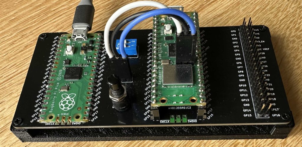
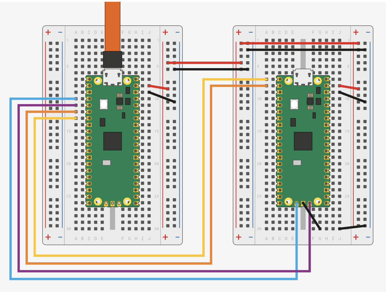
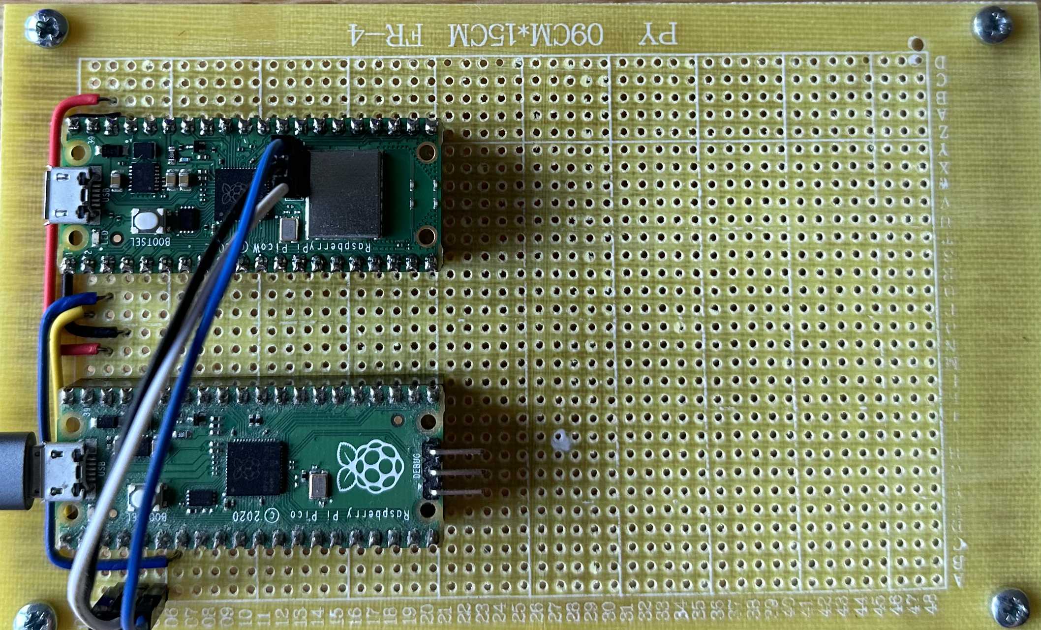
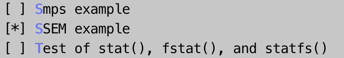
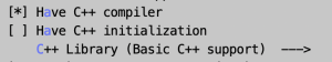
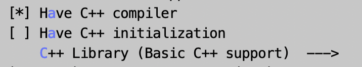
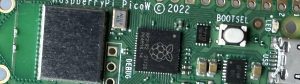
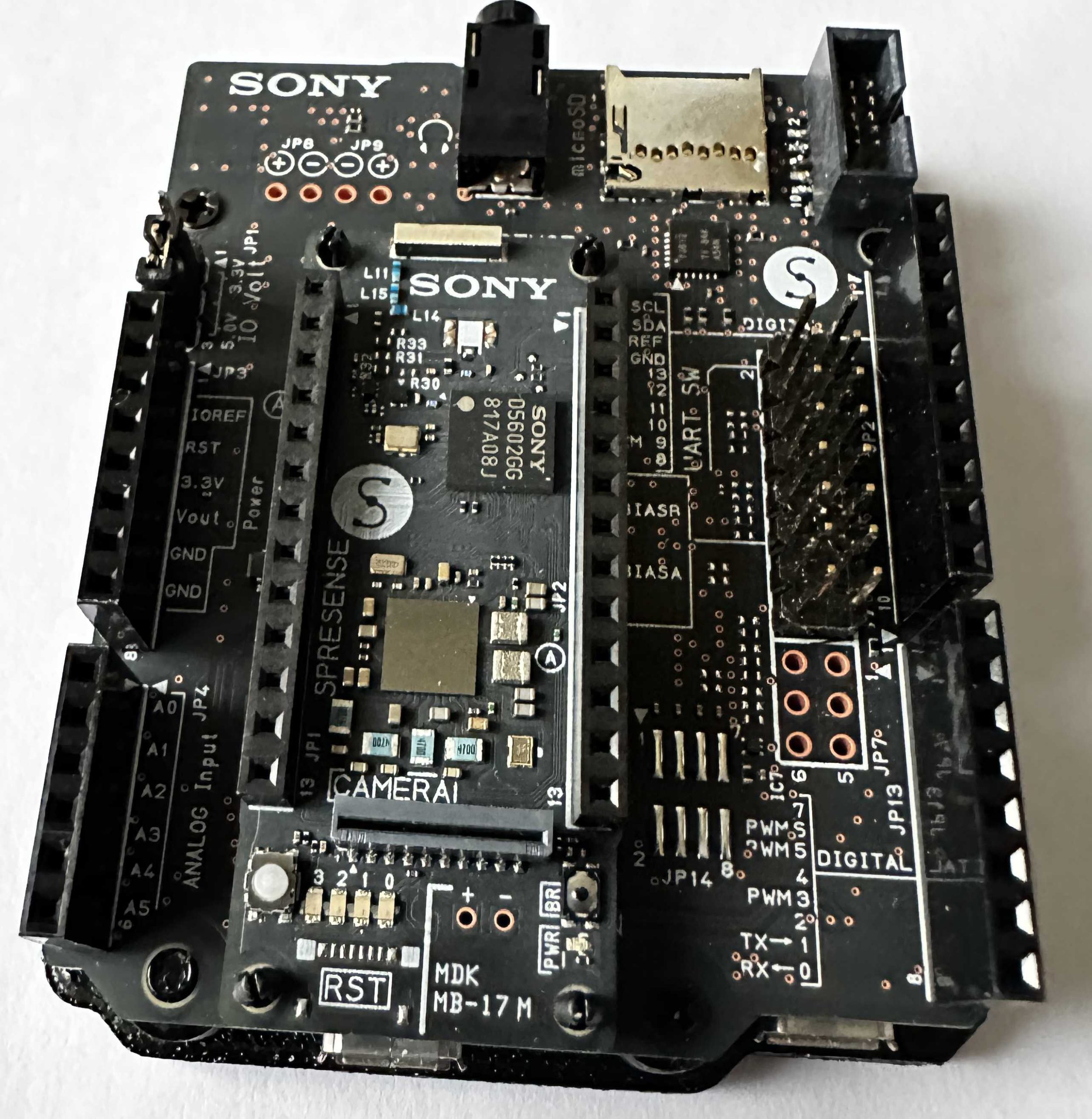
The long term aim of this port is to provide a way of running the application on a Raspberry Pi Pico connected to hardware which will emulate the original SSEM. The application on the Raspberry Pi Pico will target the NuttX RTOS. As we will see later, compiling and running on NuttX will present some interesting issues.
Initial Port
The first stage of the port is to reproduce the core functionality of the SSEM showing the application output in a console interface targeting C++ 17. The only real complication here is ensure the user interface and platform specific code are abstracted to keep as much functionality in common with a desktop and NuttX implementation as possible.
The original Python code and the C++ port can be found in the Manchester Baby GitHub repository. A quick check of the source code shows that the 1:1 mapping has been kept where possible. The only real significant difference between the two code bases is the separation of the unit tests from the class implementation. The Python code keeps the unit test code in the class definitions themselves, the C++ code implements the unit tests in their own files.
Memory Checks
The switch from Python to C++ brings a new danger, memory access issues and memory leaks.
One memory issue that we can address relatively easily is memory leaks. If we can abstract the core functionality into a self contained group of files then we can use valgrind to check for memory leaks. A small glitch with using valgrind is that the application is not available for Mac from the key repositories. There is an informal project on GitHub.
The issue of valgrind not running on the mach was resolved by putting together a Dockerfile containing common development tools. The memory check could then be run on the desktop using Docker.
Running the Emulator
The emulator can be run on both a desktop computer as well as a board running NuttX.
Run from the Desktop
Running the application on the desktop is the simplest way to test the emulator:
- Open a command console and change to the Desktop directory in the repository
- Build the emulator with the command make
- Run the emulator with the command ./ssem_main
Run on NuttX
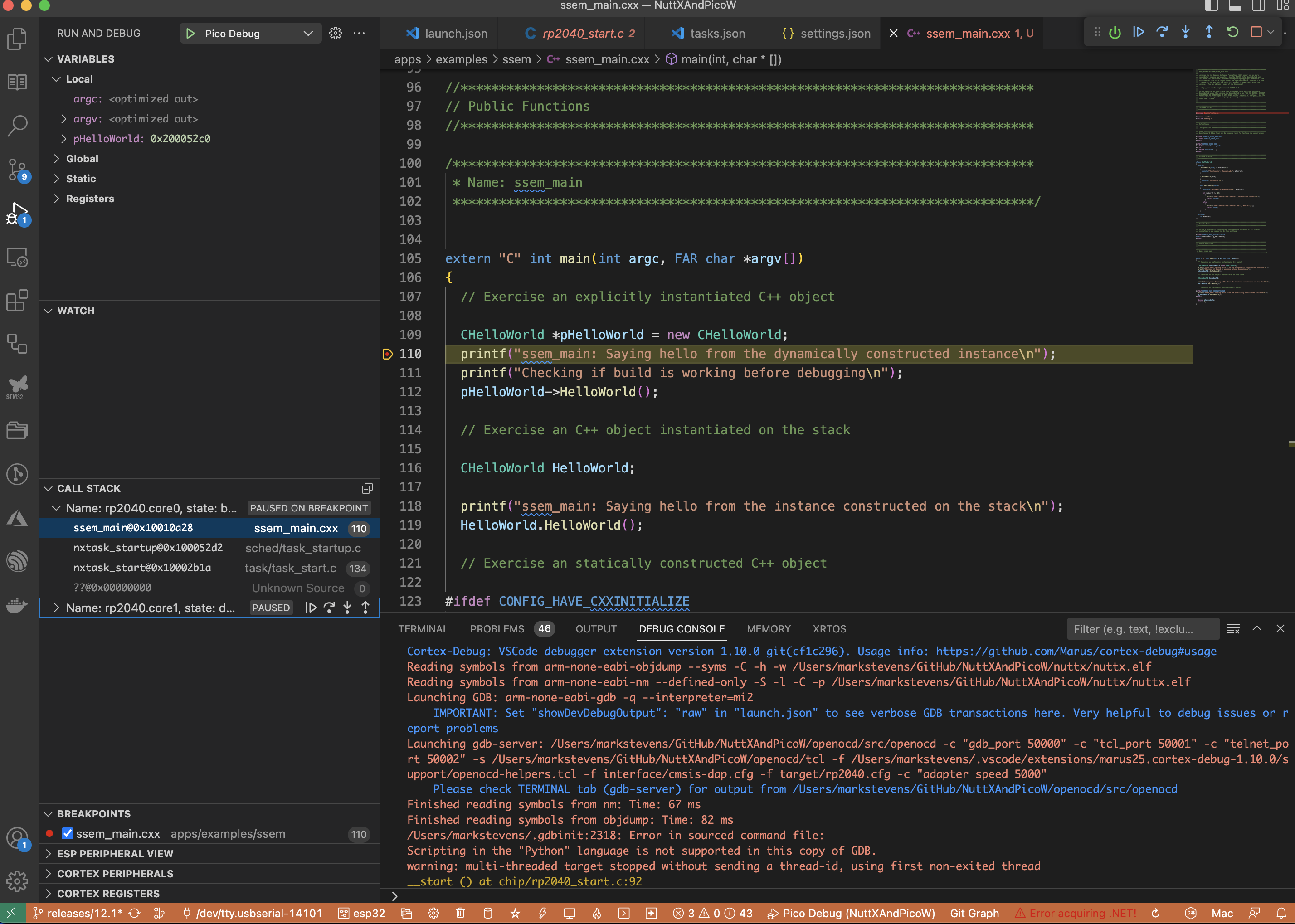
Running on NuttX is a little more complex as we need to build the application and the operating system and then deploy the binary to a board. The processes of adding the SSEM application to a Raspberry Pi PicoW board has already been documented in the article Adding a User Application to NuttX. The first step is to follow the steps in the article to add the SSEM basic applicatiom.
The next stage is to copy the contents of the NuttX directory over the application directory created in the above article. The code should then be rebuilt with the command make clean && make -j. The application can now be deployed to the board.
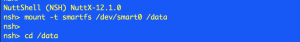
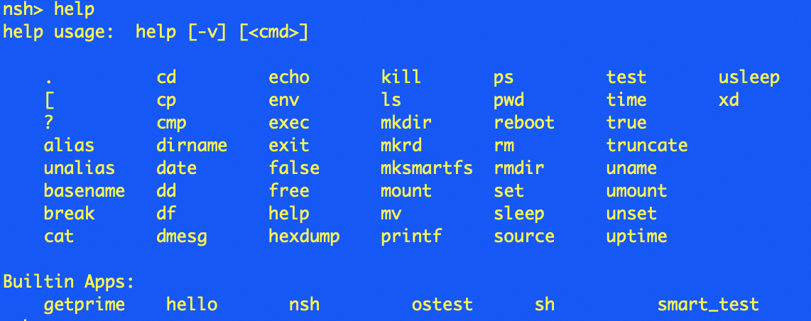
Now we have the OS and the application deployed to the Raspberry Pi (or your board of choice) we can connect a serial adapter to the board and press the enter key twice. This will bring up the NuttX shell. Typing help should show the ssem application deployed to the board. Simply execute this by entering the command ssem.
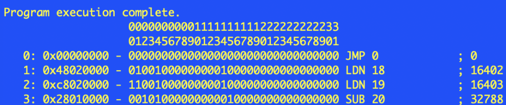
Application Output
In both cases the emulator should run the hfr989.ssem application (the source for this can be found in the SSEMApps folder in the repository). Both the desktop and the NuttX versions of the emulator will run the SSEM application and will show the start and end state of the SSEM on the console / serial port. The first output will show the SSEM application loaded into the store lines:
NuttShell (NSH) NuttX-10.4.0
nsh> ssem
                   00000000001111111111222222222233
                   01234567890123456789012345678901
   0: 0x00000000 - 00000000000000000000000000000000 JMP 0            ; 0
   1: 0x48020000 - 01001000000000100000000000000000 LDN 18           ; 16402
   2: 0xc8020000 - 11001000000000100000000000000000 LDN 19           ; 16403
   3: 0x28010000 - 00101000000000010000000000000000 SUB 20           ; 32788
   4: 0x00030000 - 00000000000000110000000000000000 CMP              ; 49152
   5: 0xa8040000 - 10101000000001000000000000000000 JPR 21           ; 8213
   6: 0x68010000 - 01101000000000010000000000000000 SUB 22           ; 32790
   7: 0x18060000 - 00011000000001100000000000000000 STO 24           ; 24600
   8: 0x68020000 - 01101000000000100000000000000000 LDN 22           ; 16406
   9: 0xe8010000 - 11101000000000010000000000000000 SUB 23           ; 32791
  10: 0x28060000 - 00101000000001100000000000000000 STO 20           ; 24596
  11: 0x28020000 - 00101000000000100000000000000000 LDN 20           ; 16404
  12: 0x68060000 - 01101000000001100000000000000000 STO 22           ; 24598
  13: 0x18020000 - 00011000000000100000000000000000 LDN 24           ; 16408
  14: 0x00030000 - 00000000000000110000000000000000 CMP              ; 49152
  15: 0x98000000 - 10011000000000000000000000000000 JMP 25           ; 25
  16: 0x48000000 - 01001000000000000000000000000000 JMP 18           ; 18
  17: 0x00070000 - 00000000000001110000000000000000 HALT             ; 57344
  18: 0x00000000 - 00000000000000000000000000000000 JMP 0            ; 0
  19: 0xc43fffff - 11000100001111111111111111111111 HALT             ; -989
  20: 0x3bc00000 - 00111011110000000000000000000000 JMP 28           ; 988
  21: 0xbfffffff - 10111111111111111111111111111111 HALT             ; -3
  22: 0x243fffff - 00100100001111111111111111111111 HALT             ; -988
  23: 0x80000000 - 10000000000000000000000000000000 JMP 1            ; 1
  24: 0x00000000 - 00000000000000000000000000000000 JMP 0            ; 0
  25: 0x08000000 - 00001000000000000000000000000000 JMP 16           ; 16
  26: 0x00000000 - 00000000000000000000000000000000 JMP 0            ; 0
  27: 0x00000000 - 00000000000000000000000000000000 JMP 0            ; 0
  28: 0x00000000 - 00000000000000000000000000000000 JMP 0            ; 0
  29: 0x00000000 - 00000000000000000000000000000000 JMP 0            ; 0
  30: 0x00000000 - 00000000000000000000000000000000 JMP 0            ; 0
  31: 0x00000000 - 00000000000000000000000000000000 JMP 0            ; 0
Reading from left to right, the above output shows the following:
- Store line number (i.e. the memory address) 0:, 1: etc.
- The hexadecimal representation of the store line contents.
- Binary representation of the store line contents
- Disassembled representation of the store line contents JMP 0 etc.
- Decimal representation of the store line contents
It must be remembered when reading the above that the least significant bit is at the left of the word and the most significant bit is to the right. This is honoured with the hexadecimal and binary components of the above output. The decimal value to the right should be read in the usual way for a base 10 number.
After a short time the contents of the store lines at the end of the run will be displayed:
Program execution complete.
                   00000000001111111111222222222233
                   01234567890123456789012345678901
   0: 0x00000000 - 00000000000000000000000000000000 JMP 0            ; 0
   1: 0x48020000 - 01001000000000100000000000000000 LDN 18           ; 16402
   2: 0xc8020000 - 11001000000000100000000000000000 LDN 19           ; 16403
   3: 0x28010000 - 00101000000000010000000000000000 SUB 20           ; 32788
   4: 0x00030000 - 00000000000000110000000000000000 CMP              ; 49152
   5: 0xa8040000 - 10101000000001000000000000000000 JPR 21           ; 8213
   6: 0x68010000 - 01101000000000010000000000000000 SUB 22           ; 32790
   7: 0x18060000 - 00011000000001100000000000000000 STO 24           ; 24600
   8: 0x68020000 - 01101000000000100000000000000000 LDN 22           ; 16406
   9: 0xe8010000 - 11101000000000010000000000000000 SUB 23           ; 32791
  10: 0x28060000 - 00101000000001100000000000000000 STO 20           ; 24596
  11: 0x28020000 - 00101000000000100000000000000000 LDN 20           ; 16404
  12: 0x68060000 - 01101000000001100000000000000000 STO 22           ; 24598
  13: 0x18020000 - 00011000000000100000000000000000 LDN 24           ; 16408
  14: 0x00030000 - 00000000000000110000000000000000 CMP              ; 49152
  15: 0x98000000 - 10011000000000000000000000000000 JMP 25           ; 25
  16: 0x48000000 - 01001000000000000000000000000000 JMP 18           ; 18
  17: 0x00070000 - 00000000000001110000000000000000 HALT             ; 57344
  18: 0x00000000 - 00000000000000000000000000000000 JMP 0            ; 0
  19: 0xc43fffff - 11000100001111111111111111111111 HALT             ; -989
  20: 0x54000000 - 01010100000000000000000000000000 JMP 10           ; 42
  21: 0xbfffffff - 10111111111111111111111111111111 HALT             ; -3
  22: 0x6bffffff - 01101011111111111111111111111111 HALT             ; -42
  23: 0x80000000 - 10000000000000000000000000000000 JMP 1            ; 1
  24: 0x00000000 - 00000000000000000000000000000000 JMP 0            ; 0
  25: 0x08000000 - 00001000000000000000000000000000 JMP 16           ; 16
  26: 0x00000000 - 00000000000000000000000000000000 JMP 0            ; 0
  27: 0x00000000 - 00000000000000000000000000000000 JMP 0            ; 0
  28: 0x00000000 - 00000000000000000000000000000000 JMP 0            ; 0
  29: 0x00000000 - 00000000000000000000000000000000 JMP 0            ; 0
  30: 0x00000000 - 00000000000000000000000000000000 JMP 0            ; 0
  31: 0x00000000 - 00000000000000000000000000000000 JMP 0            ; 0
Executed 21387 instructions in 30000000 nanoseconds
The original SSEM ran at about 700 instructions per second, modern PCs and even RP2040 processors are running the application much faster.
Conclusion
Even small boards (such as the Raspberry Pi Pico) running relatively low power processors can now emulate the Manchester Baby running application intended for the SSEM many times faster that the original hardware. The hfr989.ssem application would have run in about 30 seconds in 1948, today we can run this in an emulator in less that 30ms.