RSS

Archive for August, 2012

Converting The Way of The Register Examples

Friday, August 31st, 2012

A few days ago I was discussing a post from this series in the Netduino chat room with someone who is following the posts and is keen to learn about the STM8S. It became apparent that there are a few things I am taking for granted; namely:

  • Assuming you all have the same hardware set up as me
  • You are familiar with the development environment I am using

For the hardware case this is certainly unlikely especially with the availability and low pricing of the STM8S Discovery boards. As for the software, well there are at least two environments available and a number of compilers and assemblers.

The objective of this post is to describe the environment I am using and how you can convert the hardware and software setup to work with the STM8S Discovery board. By converting the application to this board we will cover the principle steps which should be followed in order to convert the application to run on any of the STM8S family of microcontrollers. We will also cover some of the shortcut keys in the development environment in order to help the novice/infrequent user of the environment become a little more productive.

For the purposes of this exercise we will look at the Simple GPIO example as this application is small and simple.

Hardware

The first thing we will do is look at the hardware I am using and then compare this to the STM8S Discovery board.

My Hardware Configuration

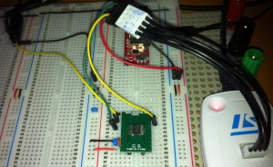
I am using the STM8S103F3P3 in a TSSOP20 package. This has been mounted on a TSSOP20 to DIP board to allow me to insert the chip into a breadboard circuit. When mounting this on a breadboard you need the following components:

  • 2 x 1uF capacitors (you can get away with only one for simple circuits)
  • 1 x 100nF capacitor
  • 3.3V regulated power supply
  • ST-Link/V2 programmer
  • Some wire to wire it all up.

To put this together, place one of the 1uF capacitors between VSS and VCAP and a 100 nF capacitor is placed between VDD and VSS. An additional (this is the optional capacitor) 1uF capacitor is also placed across the +3.3V and ground of the power supply.

The ST-Link/V2 should be connected to 3.3V and ground with the SWIM and NRST lines connected to the appropriate pins on the STM8S.

When you have all this put together you will have something like the following:

STM8S103 set up on Breadboard

STM8S103 set up on Breadboard

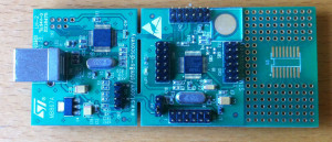
Now compare this to the STM8S Discovery board:

STM8S Discovery Board

STM8S Discovery Board

As you can see, all of the work setting up the hardware has been done for you :). You will also note that the chip used is the STM8S105C6T6. This chip is a different series to the one I am targeting. It is also a larger package giving the developer access to more ports etc. This board also has the ST-Link programmer built into the board. The only thing we need in order to use this board is a USB cable.

Development Environment

The development environment we are using is the IAR Kickstarter environment. This allows the creation of small applications (8 KBytes) for the STM8S. At the time of writing, the licence allowed the creation of fully functional applications with no commercial restrictions on the applications you create. The only requirement for the developer is that you register for a licence key.

We will not cover setting up the environment as this is a standard Windows installer.

If you have decided to use this environment then you might want to check out Custom IAR Templates for STM8S Projects. Arron Chapman has also put together some additional files and templates together. These are available in his posting Custome IAR STM8S Template.

Running the Application

We should now have the hardware and software set up so let’s take a look at the application we will be working with:

#include <iostm8S103f3.h>

int main( void )
{
    //
    //  Initialise Port D.
    //
    PD_ODR = 0;             //  All pins are turned off.
    PD_DDR_DDR5 = 1;        //  Port D, bit 5 is output.
    PD_CR1_C15 = 1;         //  Pin is set to Push-Pull mode.
    PD_CR2_C25 = 1;         //  Pin can run up to 10 MHz.
    //
    //  Now lets toggle to IO line.
    //
    while (1)
    {
        PD_ODR_ODR5 = 1;    // Turn Port D, Pin 5 on.
        PD_ODR_ODR5 = 0;    // Turn Port D, Pin 5 off.
    }
}

If you are using the STM8S103F3 chip then the application should compile and deploy OK. So now let’s consider what we need to do to make this run on the STM8S Discovery board.

The first thing to note is the include file we are using. This should match the chip you are using in your environment. You can find a full list of the include files supplied with the development environment in the inc directory of the installation. On my machine these can be found in C:Program Files (x86)IAR SystemsEmbedded Workbench 6.0 Kickstartstm8inc. If you browse through this directory you will find a file iostm8s105c6.h. This is the file you should be using for the STM8S Discovery board.

So make the change to the include file and we can now compile the application (press F7). The application should compile without any warnings or errors.

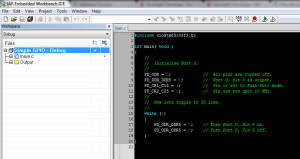
If you were to try to deploy the application now you would receive an error from the development environment. This is because the development environment and the programmer (ST-Link/V2) are targeting the wrong chip. To correct this we need to change the project options. Assuming you have your development environment open you should be looking at something like this:

Simple GPIO Project In IAR

Simple GPIO Project In IAR

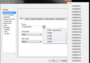
Right click on the project name in the left hand panel (Simple GPIO – Debug) and select Options. Look for the Device text on the dialog which appears and click on the button to the right of the text box which contains the text STM8S103F3P3 and follow the popups which appear and select the STM8S105C6 chip.

Using IAR Options to Change the Target Device

Using IAR Options to Change the Target Device

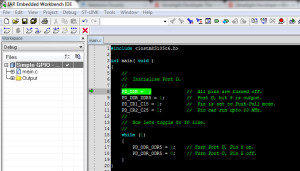
At this point we should be ready to try the application out. So make sure that the STM8S Discovery board is connected to your PC and compile and deploy the application (Ctrl-D). At this point the application compiles and deploys after which the debugger should stop at the default breakpoint which has been set for you on the first line of code. Your display should look something like the following:

Breakpoint on the first line of code in the IAR environment

Breakpoint on the first line of code in the IAR environment

The green arrow and the highlighted line indicate the next line of code to be executed. From here we have a few options open to us:

  • Run the application with no breakpoints
  • Single step through the application
  • Set some breakpoints and then run the application

These options should be familiar to any software engineer.

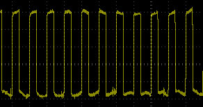
Let’s hook the STM8S Discovery board up to an oscilloscope and run the application (press F5). You should now see the following output on the oscilloscope:

Simple GPIO Running on the STM8S Discovery Board Oscilloscope Output

Simple GPIO Running on the STM8S Discovery Board Oscilloscope Output

IAR Shortcut Keys

Throughout this post we have looked at some of the shortcut keys which I commonly use. The following table shows the key and the description of its function. This is not meant to be a comprehensive list of the keys used but it covers a few of the basics which I use regularly:

KeyFunction
Ctrl-DCompile the code and deploy to the device.
Shift-Ctrl-DTerminate the debugging session.
F7Make the project, do not deploy.
F5In debug mode, causes the application to run until the next breakpoint is reached or the application terminates.
F10In debug mode, execute the currently selected statement and then break at the next line of code. This will step over any method calls.
F11As with F10 but this time step into any method calls.
Shift-F11Step out of the current method being debugged and return to the calling method with a breakpoint set accordingly.
Shift-Ctrl-RReset the debugging environment setting a breakpoint on the first line of code and restart the application.
Ctrl-KComment out the currently selected lines of code.
Shift-Ctrl-KUncomment the selected lines of code.

Conclusion

As we have shown, a few simple changes to the example code in The Way of the Register series are all we need to make to run these examples on other STM8S chips other than the STM8S103F3. In summary we need to do the following:

  • Check the include file and make sure it matches the chip you are using
  • Check the chip the development environment is targeting

Hope you have found this useful and continue to enjoy The Way of the Register series.
Generating PWM Signals using the STM8S

Thursday, August 30th, 2012

In a recent post we looked at the generation of a square wave signal using a timer and the update/overflow interrupt. There we generated a 20 Hz signal from the STM8S by toggling an output port using direct access to a port configured as an output port. In this post we will go one step further and use the capabilities of the timer to generate the pulse directly. We will also look at how we can manipulate the registers to allow the generation of a PWM pulse from the STM8S by simply changing the register values used to configure the port.

It is important that you read and understand the previous post Using Timers on the STM8S before continuing further as we will be using much of the knowledge in that post here.

So the project definition here is simple to start with, we will generate a square wave without using GPIO ports. We will then follow up on this by changing the values in the registers to generate a PWM signal with a duty cycle which can be defined by the programmer.

The Registers

The application will use most of the registers described in the previous post as well as the following:

  1. TIM2_CCR1H & TIM2_CCR1L – Capture/Compare Register 1 High/Low
  2. TIM2_CCER1 – Capture/Compare Enable register 1
  3. TIM2_CCMR1 – Capture/Compare Mode Register 1


TIM2_CCR1H & TIM2_CCR1L – Capture/Compare Register 1 High/Low

These two registers are analogous to the TIM2_ARRH and TIM2_ARRL registers. TIM2_ARRH/L are used to determine the period of the signal whilst TIM2_CCR1H/L are used to determine the duty cycle of the signal. Let us assume that we are using the value of 50,000 for TIM2_ARRH/L as in the last post then by setting TIM2_CCR1H/L to 25,000 will give a duty cycle of 50%. Similarly, setting TIM2_CCR1H/L to 12,500 with give a duty cycle of 25% (or 75%) depending upon the register settings for active high/low – see TIM2_CCER1.

TIM2_CCER1 – Capture/Compare Enable register 1

We will be using two bits in this register, Capture/Compare 1 Output Polarity (CC1P) and Capture/Compare output Enable (CC1E).

So let’s start with the easy one, CC1E. This simply enables or disables the capture/compare for channel 1 of Timer 2. Setting this to 1 enables the mode, setting this to 0 disables the mode.

On to the difficult bit of this register, namely the output polarity (CC1P). This bit determines the polarity of the active state. A value of 1 configures the active state to be low whilst a value of 0 configures the state to be high.

It is important to note here that the meaning of active is different from the meaning of a high or low signal. Let us consider a simple example, namely a PWM signal with a duty cycle of 50%. So, for 50% of the time the signal is logic 1 (high) and for 50% of the time the signal is logic 0 (low). Or another way of looking at it is that if we define high to be active and low to be inactive then for 50% of the time the signal is active and 50% of the time the signal is inactive.

CC1P allows us to define what we mean by active and inactive. Once we have the application written we can change this value and see the effect on the output.

TIM2_CCMR1 – Capture/Compare Mode Register 1

This register allows the application to change the way in which the channel is configured. In this case we will only be concerned with setting this to one of two values, namely 6 or 7.

ValueModeDescription
110 – 6PWM Mode 1In up-counting mode, the channel is active if the counter is less than CCR1, otherwise it is inactive.
In down-counting mode the channel is inactive when the counter is greater than CCR1, otherwise the channel is inactive.
111 – 7PWM Mode 2In up-counting mode the channel is inactive as long as the counter is less than CCR1.

Software

The first two things we will do is steal some code from previous posts, namely the Configuring the System Clock and Using Timers on the STM8S. We will use the InitialiseSystemClock and InitialiseTimer2 methods respectively.

The next thing we need to consider is how we set up the timer. We will continue to use Timer 2 so we can again use some of the code from previous posts. However, we need to make a few modifications to SetupTimer2 method.

So let’s start by having a 25% duty cycle (25% high, 75% low). At the moment we are not too worried about the frequency of the signal so let’s work with TIM2_ARRH/L set to 50,000 as in the previous post. This means that we want the output low for 75% of the time (37,500 counts) and high for 25% of the time (12,500 counts). Time for the first decision, let’s use PWM mode 1 (TIM2_CCMR1_OC1M = 6).

Given the default mode (down-counting) and looking at the register definition for TIM2_CCMR1_OC1M we want to define active as a logic 0 and inactive as a logic 1. So this means we need to set TIM_CCMR1_OC1M = 0.

If we put all of this together we end up with the following method:

void SetupTimer2()
{
    TIM2_PSCR = 0x00;       //  Prescaler = 1.
    TIM2_ARRH = 0xc3;       //  High byte of 50,000.
    TIM2_ARRL = 0x50;       //  Low byte of 50,000.
    TIM2_CCR1H = 0x30;      //  High byte of 12,500
    TIM2_CCR1L = 0xd4;      //  Low byte of 12,500
    TIM2_CCER1_CC1P = 0;    //  Active high.
    TIM2_CCER1_CC1E = 1;    //  Enable compare mode for channel 1
    TIM2_CCMR1_OC1M = 6;    //  PWM Mode 1 - active if counter < CCR1, inactive otherwise.
    TIM2_CR1_CEN = 1;       //  Finally enable the timer.
}

And as we are using a timer to do all of the work, our main method becomes:

void main()
{
    //
    //  Initialise the system.
    //
    __disable_interrupt();
    InitialiseSystemClock();
    InitialiseTimer2();
    SetupTimer2();
    __enable_interrupt();
    while (1)
    {
        __wait_for_interrupt();
    }
}

Let’s Look at the Output

If we look at the clock settings (16MHz) and the value for TIM2_ARR (50,000) we should be looking for a signal with a frequency of around 320 Hz (16 MHz / 50,000). So compiling the above we are expecting a 320Hz signal with a duty cycle of 25%. Here is the output on the oscilloscope:

PWM with a 25% high signal

PWM with a 25% high signal

Changing the value of TIM2_CCER1_CC1P to 1 gives the following:

PWM with a 75% high signal

PWM with a 75% high signal

As you can see, the polarity allows us to change what we mean by active.

Some ideas for you:

  1. Change TIM2_ARR values to change the frequency
  2. Change TIM2_CCR1 values to change the duty cycle

As always, the source code for this example is available for download.

Source Code Compatibility

SystemCompatible?
STM8S103F3 (Breadboard)
Variable Lab Protomodule
STM8S Discovery

Generating a Regular Pulse Using Timer 2

Wednesday, August 29th, 2012

In previous posts you may have seen an example program where we generate a 20Hz signal using the overflow interrupt on Timer 2. Here we will translate the post to use direct register access rather than use the STD Peripheral Library.

So the project definition is simple, output a regular signal (20Hz with a 50% duty cycle) on Port D, Pin 4 (i.e. pin 2 on the STM8S103F3P3).

Algorithm

To make this project a low on processor power we will use interrupts to generate the pulse. To do this we will make use of one of the STM8S timers, namely Timer 2 (T2). The algorithm becomes:

  1. Turn off the timer
  2. Setup the timer to generate an interrupt every 1 / 40th of a second
  3. Set up the output port to generate the signal.
  4. Wait for interrupts indefinitely

The Interrupt Service Routine (ISR) then has one very simple task, toggle the output port and wait for the next interrupt.

The Registers

This application is simple and really only uses a fraction of the power of the STM8S timers. In fact we can set up the chip using relatively few registers. With the exception of resetting the timer to a known state we will be using only six registers in this exercise:

  1. TIM2_PSCR
  2. TIM2_ARRH and TIM2_ARRL
  3. TIM2_IER
  4. TIM2_CR1
  5. TIM2_SR1

TIM2_PSCR – Timer 2 Prescalar

The 16-bit counter in Timer 2 receives a clock signal from the prescalar. This in turn receives a clock from the internal clock of the STM8S (i.e. fmaster). The prescalar divides the fmaster clock by the prescalar set in the TIM2_PSCR register. This allows the timer to receive a slower clock signal than that running the STM8S. The prescalar is a power of 2 and the effective frequency of the clock running Timer 2 is given by the following formula:

fcounter = fmaster / 2TIM2_PSCR

where fcounter is the frequency of the signal being used as a clock source for Timer 2.

TIM2_PSCR is a 4 bit number and this restricts the value of the prescalar to 1 to 32,768.

We will come back to this formula when we write the software in order to calculate the prescalar we will need to generate the 20Hz clock signal.

TIM2_ARRH and TIM2_ARRL – Counter Auto-Reload Registers

We will be using the counter as a simple up/down counter. We will be loading this register with a counter value which the timer will count up to / down from. An interrupt will be generated when the counter value has been reached (for up) or zero is reached (for down). The counter will then be reset using the values in these two registers.

The only important thing to note about these two registers is that TIM2_ARRH must be loaded with a value before TIM2_ARRL.

TIM2_IER – Interrupt Enable Register

This register determines which interrupts Timer2 can generate. In our case we only need one, namely the update interrupt. This is generated when the counter value has been reached.

The interrupt is enabled by setting TIM2_IER_UIE to 1.

TIM2_CR1 – Timer 2 Control Register 1

The only bit we will be interested here is the Counter ENable bit (CEN). This will be used to start the counter.

TIM2_SR1 – Timer 2 Status Register 1

This register gives us status information about the timer. There is only one bit we are interested in for this exercise and that is the Update Interrupt Flag (UIF). This bit determines if an update interrupt is pending. The bit is set by hardware but crucially it must be reset by software.

When we enter the ISR, this bit will have been set by the hardware controlling the timer. On existing the ISR the hardware will check the status of the bit. If it is set then the interrupt will be generated once more. This means that if we are not careful then we can end up in a cycle of generating an interrupt, processing the interrupt in the ISR and then generating the interrupt again ad infinitum. It is therefore crucial that this bit is cleared before the ISR is exited.

Software

One of the first things to note is that as with all of the examples we will discuss in this series, we will assume a clock running using the internal oscillator and set to 16MHz.

The code which will deal with the interrupt has a very simple job to do, namely toggle the pin we are using to generate the output pulse. One thing to note it that as we are toggling the pin in this method we will effectively be halving the output frequency of the signal which has been generated. Lets look at what is happening.

  1. ISR 1 – output is low we will make the output high.
  2. ISR 2 – output is high we will make the signal low
  3. ISR 3 – output is low we will make the signal high
  4. etc.

The frequency of the output for a regular signal is determined by the amount of time between the two rising edges of the output. So in our case, the time is double the frequency of the calls to the ISR as we toggle the output in the ISR. This is important and will be used in the calculations we make regarding the timer settings later.

The remainder of the code looks similar to that used in the external interrupts example presented in an earlier post.

//
//  Timer 2 Overflow handler.
//
#pragma vector = TIM2_OVR_UIF_vector
__interrupt void TIM2_UPD_OVF_IRQHandler(void)
{
    PD_ODR_ODR4 = !PD_ODR_ODR4;     //  Toggle Port D, pin 4.
    TIM2_SR1_UIF = 0;               //  Reset the interrupt otherwise it will fire again straight away.
}

If you have been following the series, the next piece of code should also be familiar (see the Simple GPIO example). We will be setting up Port D, pin 4 to be an output port. This is the pin which will output the signal we will be generating.

//
//  Setup the port used to signal to the outside world that a timer even has
//  been generated.
//
void SetupOutputPorts()
{
    PD_ODR = 0;             //  All pins are turned off.
    PD_DDR_DDR4 = 1;        //  Port D, pin 4 is used as a signal.
    PD_CR1_C14 = 1;         //  Port D, pin 4 is Push-Pull
    PD_CR2_C24 = 1;         //  Port D, Pin 4 is generating a pulse under 2 MHz.
}

The next method resets Timer 2 and put it into a known state. This simply requires resetting all of the Timer 2 registers to 0.

//
//  Reset Timer 2 to a known state.
//
void InitialiseTimer2()
{
    TIM2_CR1 = 0;               // Turn everything TIM2 related off.
    TIM2_IER = 0;
    TIM2_SR2 = 0;
    TIM2_CCER1 = 0;
    TIM2_CCER2 = 0;
    TIM2_CCER1 = 0;
    TIM2_CCER2 = 0;
    TIM2_CCMR1 = 0;
    TIM2_CCMR2 = 0;
    TIM2_CCMR3 = 0;
    TIM2_CNTRH = 0;
    TIM2_CNTRL = 0;
    TIM2_PSCR = 0;
    TIM2_ARRH  = 0;
    TIM2_ARRL  = 0;
    TIM2_CCR1H = 0;
    TIM2_CCR1L = 0;
    TIM2_CCR2H = 0;
    TIM2_CCR2L = 0;
    TIM2_CCR3H = 0;
    TIM2_CCR3L = 0;
    TIM2_SR1 = 0;
}

The next thing we need is a method which sets the Timer 2 to generate the interrupt. This is where we need to start doing some calculations.

So let’s start with the frequency of the clock going into the counter for Timer 2. As we have seen earlier, this is given by the following:

fcounter = fmaster / 2TIM2_PSCR

Now we also know that the interrupts will be generated every time the counter value is reached. So the frequency of the interrupt is given by the following:

finterrupt = fcounter / counter

Putting the two together we get the following:

finterrupt = fmaster / (2TIM2_PSCR * counter)

A little rearranging gives:

(2TIM2_PSCR * counter) = fmaster / finterrupt

If we plug in the numbers we know, fmaster = 16MHz and finterrupt = 40 (remember that the frequency of the signal we are generating is half the frequency of the interrupts) then we find:

(2TIM2_PSCR * counter) = 400,000

So, if we take 400,000 and divide by 50,000 (for simplicity) then we have a factor of 8. So, given that the counter is a 16-bit counter then the counter should be 50,000 and the prescalar should be 3 (23 = 8).

//
//  Setup Timer 2 to generate a 20 Hz interrupt based upon a 16 MHz timer.
//
void SetupTimer2()
{
    TIM2_PSCR = 0x03;       //  Prescaler = 8.
    TIM2_ARRH = 0xc3;       //  High byte of 50,000.
    TIM2_ARRL = 0x50;       //  Low byte of 50,000.
    TIM2_IER_UIE = 1;       //  Enable the update interrupts.
    TIM2_CR1_CEN = 1;       //  Finally enable the timer.
}

Now we have all of the component parts we simply need to call the methods to set everything up and then wait for the interrupts to fire. So our main method looks like this:

//
//  Main program loop.
//
int main( void )
{
    __disable_interrupt();
    SetupOutputPorts();
    InitialiseTimer2();
    SetupTimer2();
    __enable_interrupt();
    while (1)
    {
        __wait_for_interrupt();
    }
}

Running this application results in the following trace on the oscilloscope:

20 Hz Square Wave Output on an Oscilloscope

20 Hz Square Wave Output on an Oscilloscope

A quick look at the measurements shows that this application is generating a 20Hz signal. If you don’t have a scope then you can hook a LED (use the LED circuit from the previous article on external interrupts) through a transistor. You should be able to see the LED flicker as it is turned on and off. You could also slow down the rate of the pulses by looking at changing the prescalar or adding a counter.

As always, the source code is available for download.

Source Code Compatibility

SystemCompatible?
STM8S103F3 (Breadboard)
Variable Lab Protomodule
STM8S Discovery

Using the UART on the STM8S

Monday, August 27th, 2012

We have previously seen how to configure the STM8S using the STD Peripheral Library using both the high level API and the slightly lower level register access. In this post we will use the definitions in the iostm8s103f3.h and we will also have a look at the registers which control the UART ending with a program which uses the UART to send data to a terminal emulator on a desktop computer (in my case a PC). We must remember that while this article looks at low speed communications with a PC, the UARTs on the STM8S have a variety of uses covering other protocols other than those discussed in this article.

The definition of the problem is simple, allow the STM8S to send debug information to a terminal emulator running at 115200,n,8,1 (for all of those who remember DOS MODE commands for serial communication).

It should be noted that UART1 is not available on the STM8S Discovery board and so UART2 is used instead.

The Registers

In order to set up the UART we will need to perform the following tasks:

  1. set the parity and number of data bits
  2. set the parity
  3. set the number of stop bits
  4. setup the baud rate
  5. set the clock polarity etc.

It is important to remember that transmission and reception must both be disabled before we start to change these registers.

UART_CR1 – Data Bits and Parity

The number of data bits is selected using the M bit of CR1. This can be set to either 8 or 9 bits. We will be using 8 data bits and so will need to set UART_CR1_M to 0 (setting to 1 would enable 9 data bits).

To set the parity we would set PCEN and PS. In our case we are disabling parity so only need to worry about PCEN (Parity Control Enable). Setting this bit to 0 will disable the parity calculation.

UART_CR3 – Number of Stop Bits and Clock Settings

The number of stop bits can be set to 1, 1.5 or 2. This is controlled by setting UART_CR3_STOP to one of the following values:

ValueDescription
001 Stop bit
01Reserved
102 Stop bits
111.5 Stop bits

Next, we need to consider the clock settings.

UART_CR3_CPOL determines the idle state of the clock, 0 sets the clock low when idle, 1 sets it high when idle.

UART_CR3_CPHA determines if the data should be stable on the rising or falling edge of the signal. Setting this to 0 means the data is set on the rising edge of the clock signal. Setting this to 1 means the data is ready on the falling edge of the clock signal.

UART_CR3_LBCL determines if the clock pulse for the last data bit is set to the clock pin. A 0 means the last clock pulse is not generated while 1 means that the pulse is generated.

UART_BRR1 & UART_BRR2 – Baud Rate Registers

The baud rate of the UART is controlled by dividing fmaster by the baud rate divisor. The result gives the clock speed of the serial port. In our case we have a 16 MHz clock speed for the microcontroller and we want the serial port to run at 115200 baud. So some simple rearranging of the formula and the UART divider is given by:

UART Divider= fmaster / baud rate
= 16,000,000 / 115,200
= 138
= 0x008a

Now we need to rearrange the number 0x008a a little in order to get the right bits into BRR1 and BRR2 (Baud Rate Register 1 & 2). This was written as a 32 bit number to illustrate how this is put into the registers. To do this we split the number (represented by d3d2d1d0) into three parts:

  • the first digit (d3) – 0
  • the next two digits (d2d1) – 08
  • the last digit (d0) – a

And set up the registers as follows:

BRR1= d2d1
= 0x08
BRR2= d3d0
= 0x0a

When setting these registers it is important to remember to set BRR2 before setting BRR2.

UART_CR2 & UART_CR3 – Enabling the UART

The first action we would need to take is to disable the UART and the last thing we should do is enable it. This is controlled by three bits in two different registers, namely registers UART_CR3 and UART_CR2. All three bits use 0 for disable and 1 for enable. The bits we been to set are:

UART_CR2_TENEnable/disable transmission
UART_CR2_RENEnable/disable reception
UART_CR3_CKENEnable/disable the clock

In our case we do not need to enable the output of the system clock or reception. The software below will enable these anyway in order to provide a generic serial initialisation method which can be using a variety of circumstances.

Software

Moving on to our software, we will need a standard STM8 project for the microcontroller you are using. I am using the STM8S103F3P3 and the default project I set up in a previous article.

Setting Up the UART

This code makes a fundamental assumption, namely that you have configured the chip and your circuit to run at 16 MHz. I did this by setting the chip to use the internal oscillator as its clock source and using a prescalar of 1 (see the previous article on setting up the system clock for more information). The code for this is in the InitialiseSystemClock method.

The next step is to configure the UART. This is performed in the InitialiseUART method.

//
//  Setup the UART to run at 115200 baud, no parity, one stop bit, 8 data bits.
//
//  Important: This relies upon the system clock being set to run at 16 MHz.
//
void InitialiseUART()
{
    //
    //  Clear the Idle Line Detected bit in the status register by a read
    //  to the UART1_SR register followed by a Read to the UART1_DR register.
    //
    unsigned char tmp = UART1_SR;
    tmp = UART1_DR;
    //
    //  Reset the UART registers to the reset values.
    //
    UART1_CR1 = 0;
    UART1_CR2 = 0;
    UART1_CR4 = 0;
    UART1_CR3 = 0;
    UART1_CR5 = 0;
    UART1_GTR = 0;
    UART1_PSCR = 0;
    //
    //  Now setup the port to 115200,n,8,1.
    //
    UART1_CR1_M = 0;        //  8 Data bits.
    UART1_CR1_PCEN = 0;     //  Disable parity.
    UART1_CR3_STOP = 0;     //  1 stop bit.
    UART1_BRR2 = 0x0a;      //  Set the baud rate registers to 115200 baud
    UART1_BRR1 = 0x08;      //  based upon a 16 MHz system clock.
    //
    //  Disable the transmitter and receiver.
    //
    UART1_CR2_TEN = 0;      //  Disable transmit.
    UART1_CR2_REN = 0;      //  Disable receive.
    //
    //  Set the clock polarity, lock phase and last bit clock pulse.
    //
    UART1_CR3_CPOL = 1;
    UART1_CR3_CPHA = 1;
    UART1_CR3_LBCL = 1;
    //
    //  Turn on the UART transmit, receive and the UART clock.
    //
    UART1_CR2_TEN = 1;
    UART1_CR2_REN = 1;
    UART1_CR3_CKEN = 1;
}

We will need to provide a method of sending a simple string to the serial port. The algorithm is simple:

  1. Set a pointer to the start of the string
  2. If the character pointed to be the pointer is not a null (i.e. 0) character then
    1. Transfer the character pointed to be the pointer into the UART data register
    2. Wait until the data register has been sent (Transmission Empty is true)
    3. Move the pointer on one byte

//
//  Send a message to the debug port (UART1).
//
void UARTPrintf(char *message)
{
    char *ch = message;
    while (*ch)
    {
        UART1_DR = (unsigned char) *ch;     //  Put the next character into the data transmission register.
        while (UART1_SR_TXE == 0);          //  Wait for transmission to complete.
        ch++;                               //  Grab the next character.
    }
}

And finally we need a main program to control the application.

//
//	Main program loop.
//
void main()
{
	__disable_interrupts();
	InitialiseSystemClock()
    InitialiseUART()
	__enable_interrupts();
	while (1)
	{
        UARTPrintF("Hello from my microcontroller....\n\r");
		for (long counter = 0; counter < 250000; counter++);
	}
}

The full application code can be downloaded from here. Simply unzip the files and open the project with IAR. The application can be downloaded to the chip by pressing Ctrl-D. Once downloaded to the microcontroller press F5 to run the application.

This application has been tested on my reference platform, the Variable Labs Protomodule and the STM8S Discovery board.

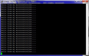
To check the application is working, connect the Tx line of the STM8S (in my case pin 2) to the Rx line on a PC which can accept 3.3V TTL logic signals. This is important, the port must accept 3.3V TTL and NOT standard RS232 signals. To do this I use a 3.3V FTDI cable and connect this to the STM8S and one of the USB ports on my PC. This gives me a COM port which I can connect to devices running at 3.3V. Now open up a terminal emulator (I used PuTTY) and connect to the com port using the correct protocol. You should see the following output:

Output from the STM8S shown on a PuTTY terminal

Output from the STM8S shown on a PuTTY terminal

Conclusion

Adding these methods to you project should allow you to generate debug output from an application running on the STM8S or communicate with devices which are controlled using a serial communication protocol.

Source Code Compatibility

SystemCompatible?
STM8S103F3 (Breadboard)
Variable Lab Protomodule
STM8S Discovery

External Interrupts on the STM8S

Thursday, August 16th, 2012

In a previous post we looked at the GPIO pins and how we could set the pins to either input or output but we concentrated on output. In this post we will look at using interrupts to detect input from the user and an output to indicate that the input has been detected. Our objective is:

  1. Create a circuit which can register when a button has been pressed.
  2. Toggle a LED when the button is pressed

Should be simple, so let’s give it a go.

Hardware

For the hardware we will need three components:

  1. STM8S Circuit
  2. Switch
  3. LED

STM8S Circuit

For the STM8S we need the STM8S103F3 connected to 3.3V and ground. We will also need to add two ceramic capacitors, a 100nF between Vss and Vdd (pins 7 and 9) and a 1uF between Vss and Vcap (pins 7 and 8).

Switch Circuit

For the switch circuit we need a switch and a pull-up resistor. We will pull the input line to the STM8S high through the pull-up resistor. Pressing the switch will pull the input line low. This part of the circuit looks like this:

This circuit will have the pin held high until the switch is pressed. All we need to do is to detect the falling edge of the input to the STM8S and we have a way to detecting when the user presses the switch.

One thing to note here is that we will be ignoring switch bounce and so we are likely to get the odd spurious message. We will come back to this later.

LED Circuit

This circuit is a simple transistor circuit which is used to switch on a LED. By applying a low current to the base of a transistor we can switch on a larger current to drive the LED. A quick simple circuit looks like this:

By setting a GPIO pin connected to the base of the transistor to high we can turn on a LED.

Putting it all together, we connect the switch to PD4 and the LED to PD3.

Software

The software is a simple extension of the previous post on GPIO pins. Here we are going to use the same port (port D) for both input and output. The full code is:

#include <intrinsics.h>
#include <iostm8s103f3.h>

//
//  Process the interrupt generated by the pressing of the button on PD4.
//
#pragma vector = 8
__interrupt void EXTI_PORTD_IRQHandler(void)
{
    PD_ODR_ODR3 = !PD_ODR_ODR3;     //  Toggle Port D, pin 3.
}

//
//  Main program loop.
//
void main()
{
    //
    //  Initialise the system.
    //
    __disable_interrupt();
    PD_ODR = 0;             //  All pins are turned off.
    PD_DDR = 0xff;          //  All pins are outputs.
    PD_CR1 = 0xff;          //  Push-Pull outputs.
    PD_CR2 = 0xff;          //  Output speeds up to 10 MHz.
    //
    //  Now configure the input pin.
    //
    PD_DDR_DDR4 = 0;        //  PD4 is input.
    PD_CR1_C14 = 0;         //  PD4 is floating input.
    //
    //  Set up the interrupt.
    //
    EXTI_CR1_PDIS = 2;      //  Interrupt on falling edge.
    EXTI_CR2_TLIS = 0;      //  Falling edge only.
    __enable_interrupt();

    while (1)
    {
        __wait_for_interrupt();
    }
}

So let’s start and break the program down. The first thing you will notice is that we initially configure all of the pins on port D as outputs as we have previously seen:

PD_ODR = 0;             //  All pins are turned off.
PD_DDR = 0xff;          //  All pins are outputs.
PD_CR1 = 0xff;          //  Push-Pull outputs.
PD_CR2 = 0xff;          //  Output speeds up to 10 MHz.

The next thing we do is to set up the system to allow PD4 as an input pin:

PD_DDR_DDR4 = 0;        //  PD4 is input.
PD_CR1_C14 = 0;         //  PD4 is floating input.

The final step of the configuration is to set the external interrupt for the port to detect the falling edge of the signal:

EXTI_CR1_PDIS = 2;      //  Interrupt on falling edge.
EXTI_CR2_TLIS = 0;      //  Falling edge only.

The final part of the main program is to wait for an interrupt. This is repeated infinitely:

while (1)
{
    __wait_for_interrupt();
}

The interesting part of the problem is the interrupt routine as this is where the real work is actually done. The code is simple enough you just have to make sure that you declare the method correctly:

#pragma vector = 8
__interrupt void EXTI_PORTD_IRQHandler(void)
{
    PD_ODR_ODR3 = !PD_ODR_ODR3;     //  Toggle Port D, pin 3.
}

The first two lines declare the method as an Interrupt Service Routine (ISR). The #pragma vector = 8 tells the compiler which interrupt this method will be servicing. In this case, this method will be called to process the interrupts for Port D. We will look into ISRs a little more in a later post.

Putting it all Together

If we wire all of the hardware together on a breadboard we end up with something like the following:

and a quick video of it working:

Switch Bounce

As noted earlier, mechanical switches are susceptible to switch bounce. This is caused by the mechanical contacts not closing perfectly when the switch is pressed. You can notice an example of bounce in the above video. When the switch is pressed the second time you can see that the LED is switched off but it is then switched on straight away. This is the effect of the switch contacts causing multiple signals. If a scope is hooked up to a switch you see something like the following:

In this case the switch is held down and then released. Notice the spike; this is caused by the switch bounce. If the signal is large enough then the microcontroller will think that the switch has been pressed twice rather than once – in fact that is what happened in the above video. There are a few ways to solve this but I’ll leave that as an exercise to the reader.

You can find the full source for the above project here. This application has been tested on tmy reference platform, the Variable Labs Protomodule and the STM8S Discovery board.

Compatibility

System Compatible?
STM8S103F3 (Breadboard)
Variable Lab Protomodule
STM8S Discovery

Custom IAR Templates for STM8S Projects

Thursday, August 9th, 2012

I have been using the IAR development environment to develop code for the STM8S chip for several months now. One of the things that has been a little bit of an annoyance is the need to keep reconfiguring each new project as it is created. One option would be to create a template project and keep copying the template and just rename the project files and add it to a new workspace. There must be a better way…

This is the thought which started me delving into the way in which IAR stores it’s templates and asking if I could make my own.

Where are the Templates

So the first thing to do is to work out if the templates are stored as files and if so where they are. Breaking out Explorer I found an interesting directory which looked like it might be a candidate, namely:

C:Program Files (x86)\IAR Systems\Embedded Workbench 6.0 Kickstartstm\configtemplateproject

I remembered that when you create a new IAR project you are presented with three options:

  1. asm
  2. C
  3. C++

Guess what, in that directory I found three directories and three files with the extension .projtempl. For each project name in the default projects (asm, C, C++) there was a matching directory and matching file. We may be in luck.

What’s in the Files?

The .projtempl files are pretty small so I guessed they were text files of some sort. Feeding them to Notepad++ confirmed that they were indeed text files. In fact they were XML files. In fact the default C file looks like this:

<?xml version="1.0" encoding="iso-8859-1"?>

<template>
  <displayname>C</displayname>
    <description>Creates a C project.
    </description>
  <files>
    <file>$PROJ_DIR$main.c</file>
  </files>
</template>

So my guess is that the displayname and description fields determine what is shown to the user and the files section tells the environment what files are to be included in the project.

What’s in the Directory?

Next port of call is the directory for the project. So continuing with the C project type we find that the C directory contains two files:

  1. main.c
  2. templproj.ewp

Looking inside the main.c file we find the default code which is placed inside the main.c file which is created for you when you ask for a new C project.

Putting it all together

If we put all of the pieces together, I think that we can create out own project templates using the default C project as an example. Note that I am using the C project type as an example as it is the only high level language version supported by the Kickstart edition of the IAR programming environment for the STM8S processor.

So I think we need to do the following in order to create our own template:

  1. Copy the default C directory and templproj file and give them a consistent name (i.e. the name of the directory matches the root of the file name)
  2. Edit the templproj file and change the displayname, the description and optionally the files section to match our new project type
  3. Add files to the new directory and edit any existing files as required

So let’s give it a go and see what happens.

Creating a New Template

So the first thing to do is to decide on the name of the template we are creating and copy the files. I decided on the imaginative name of My Default C Project for the new template. Catchy isn’t it.

One of the first problems I encountered was the fact that this is a system directory as far as Windows 7 is concerned and so I had to modify the permissions. If you hit any problems with this step of any others you need to make sure that you change the permissions to allow editing and creating files. I came across this on a few occasions. If you don’t know how to do this then Google your OS to find out how to change permissions. I gave Full Control access to myself for the duration of the task and changed the permissions back afterwards.

So at this point I have a My Default C Project.templproj file and a My Default C Project directory. The directory contains the same files as the C directory.

Next step, edit the templproj file and change the displayname and the description entries. I made the displayname match the directory and project file names. The description field expands on this a little more explaining what is included in the project.

Moving on to the main.c file in our new directory I edited this to contain a basic C program which included some basic headers and reset the system clock:

#include <intrinsics.h>
#include <iostm8s103f3.h>

//
//  Setup the system clock to run at 16MHz using the internal oscillator.
//
void InitialiseSystemClock()
{
    CLK_ICKR = 0;                       //  Reset the Internal Clock Register.
    CLK_ICKR_HSIEN = 1;                 //  Enable the HSI.
    CLK_ECKR = 0;                       //  Disable the external clock.
    while (CLK_ICKR_HSIRDY == 0);       //  Wait for the HSI to be ready for use.
    CLK_CKDIVR = 0;                     //  Ensure the clocks are running at full speed.
    CLK_PCKENR1 = 0xff;                 //  Enable all peripheral clocks.
    CLK_PCKENR2 = 0xff;                 //  Ditto.
    CLK_CCOR = 0;                       //  Turn off CCO.
    CLK_HSITRIMR = 0;                   //  Turn off any HSIU trimming.
    CLK_SWIMCCR = 0;                    //  Set SWIM to run at clock / 2.
    CLK_SWR = 0xe1;                     //  Use HSI as the clock source.
    CLK_SWCR = 0;                       //  Reset the clock switch control register.
    CLK_SWCR_SWEN = 1;                  //  Enable switching.
    while (CLK_SWCR_SWBSY != 0);        //  Pause while the clock switch is busy.
}

//
//  Main program loop.
//
void main()
{
    //
    //  Initialise the system.
    //
    __disable_interrupt();
    InitialiseSystemClock();
    __enable_interrupt();
}

So What Does This Do?

Next step, fire up IAR and create a new project. Guess what….

IT’S THERE !

Selecting the new project prompts me to create a new workspace (which I do) and then opens up the main.c file. Sure enough, it matches the code I have entered into the new template.

What’s Next?

Next step is to try and edit the templproj.ewp file in the C directory and set up some of the default options. For instance, I always use ST-Link/V2 to deploy to the STM8S chip. Maybe try adding a few files to the directory and the .projtempl file. The rest, as they say, is left as an exercise for the reader.