Last year I was given the Elektor FPGA board as a present. I had been wanting to work with FPGA as it presented a quick way of prototyping digital circuits and exploring the world of digital electronics. The board has been sitting in my parts collection for about 10 months. I have followed the tutorials in the magazine and decided that VHDL is probably the best way for me to start and use this board.
This post looks at my first attempt to simulate a 1-bit full adder with carry using binary logic implemented in VHDL.
I should also say that this is an early (i.e. inexperienced) project for me.
Software
Elektor recommended the Xilinx WebPack ISE software package for use with their board. It is free to use and all of their tutorials use this software. The version 14.7 download comes in at a heavy 6.17GB so make sure you have a good connection to the web or plenty of time to spare.
Project Specification
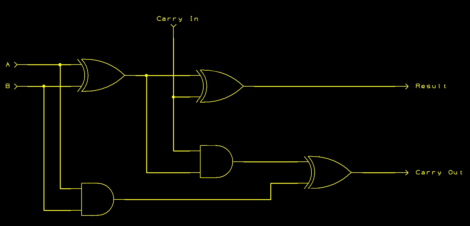
For the purpose of this exercise we will be implementing a 1-bit full adder with carry. For those not familiar with this circuit the schematic is as follows:
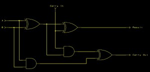
1-Bit Full Adder Schematic
The circuit takes three bits, A, B and a carry bit. The three bits are added and two bits are output from the adder, the result bit and a carry bit. The logic table for the circuit is:
| A | B | Carry In | Result | Carry Out |
| 0 | 0 | 0 | 0 | 0 |
| 0 | 1 | 0 | 1 | 0 |
| 1 | 0 | 0 | 1 | 0 |
| 1 | 1 | 0 | 0 | 1 |
| 0 | 0 | 1 | 1 | 0 |
| 0 | 1 | 1 | 0 | 1 |
| 1 | 0 | 1 | 0 | 1 |
| 1 | 1 | 1 | 1 | 1 |
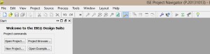
Time for start Webpack ISE.
ISE Project
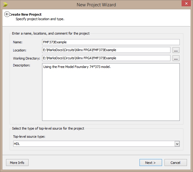
First thing to do after starting Webpack ISE is to create a new project to hold the circuit. From the startup screen select New Project
ISE Project Navigator Start Up
Now give the project a name. I selected BitFullAdderWithCarry. I actually wanted 1-Bit but ISE does not seem to like projects containing non-alpha characters. I provided a short description of the project in the Descriptionbox. Finally ensure that the project source type is set to HDL:
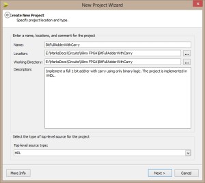
New Project Name And Properties
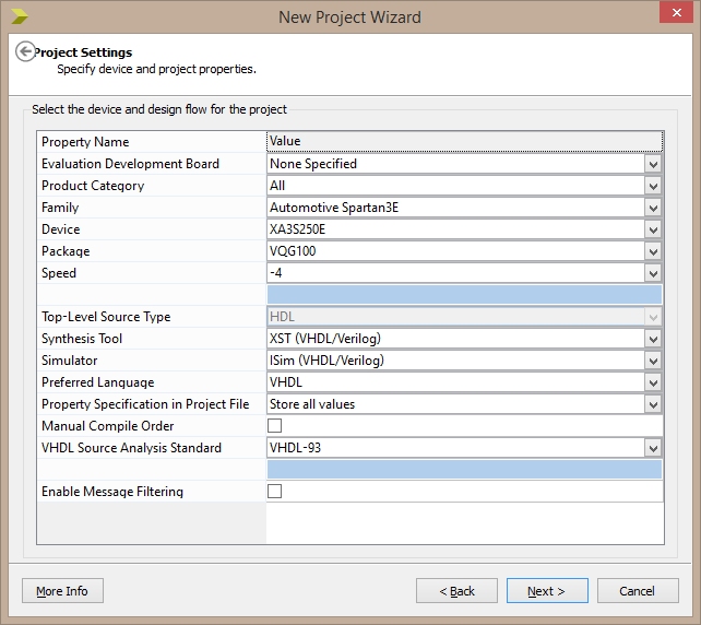
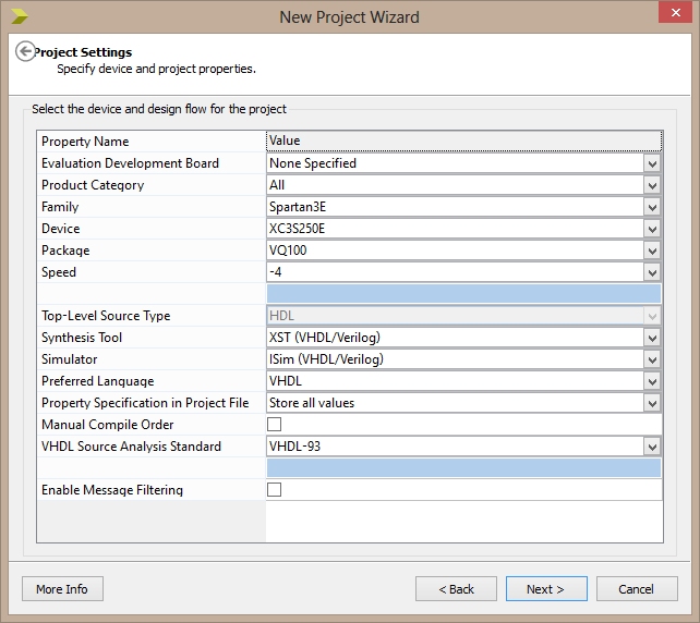
The next step is hardware specific. Here we define the target hardware characteristics. For the Elektor board we need to change the following parameters:
- Device: XC3S250E
- Package: VQ100
- Speed: -4

Device Properties
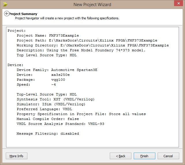
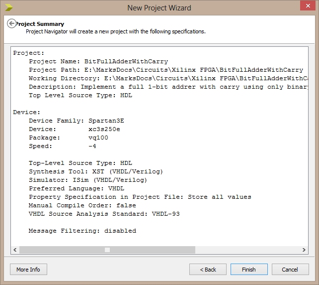
The next form simply shows the project details for review before the project is finally created.
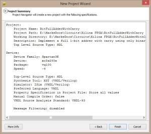
New Project Summary
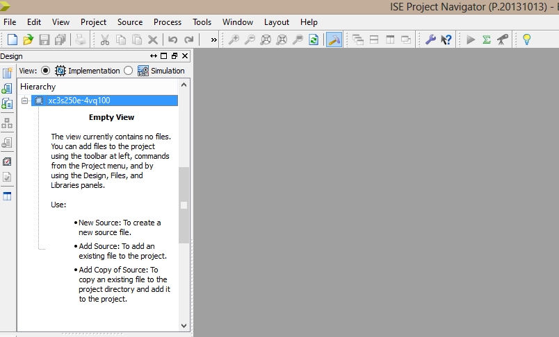
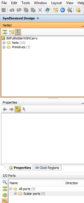
The project will now be created and is ready for the addition of files.

Empty Hierarchy
Right clicking on the device in the Hierarchy brings up the context menu which will allow the addition of new or existing files:
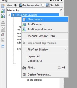
New File Menu
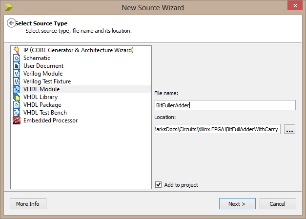
Select New Source option and a wizard will appear. In the New Source Wizard select VHDL Module and add a file name which will hold the source code for the module:

Module Type
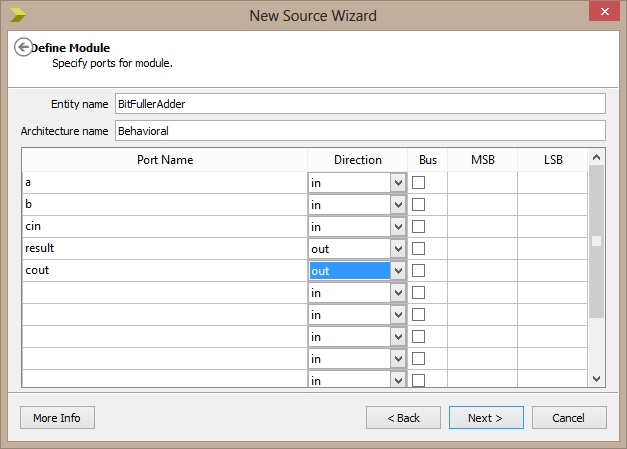
The next step is to define the ports for the module. The adder has three inputs (a, b and carry in) and two output (result and carry out). This dialog gives the option of defining the ports and their direction:
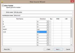
Specify Ports
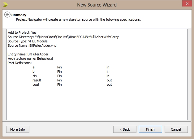
Finally a summary dialog is displayed where you can confirm the module and port information.
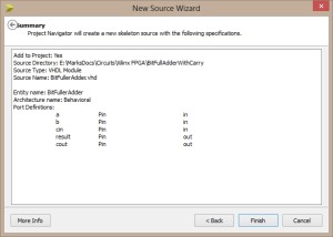
New Source Summary
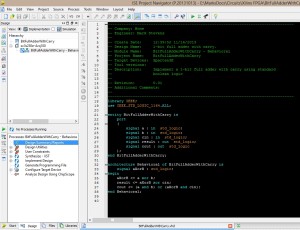
After clicking on the Finish button the new file will be added to the project along with a template for the module. The new template contains the port definitions entered in the previous dialogs, some comments and space to start entering the code to implement the module.

New Project Source Code
I must admit I find it slightly annoying that although VHDL is case insensitive, the system uses mixed case and it not consistent in it’s use. You will see what I mean when we get to testing the code.
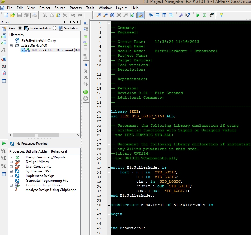
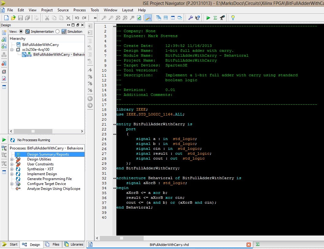
A little editing is required to get the code into a form I prefer. It is also time to add the code which implements the hardware for the full adder.
Adder Source Code
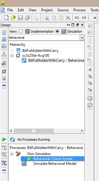
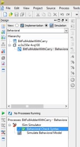
Once the code has been entered we need to perform a syntax check. Change the view in the top panel from Implementation to Simulation. Now turn your attention to the lower panel. Expand the ISIM Simulator, select Behavioural Check Syntax and click on the green triangle to start the syntax check. After a short while a green tick will appear to indicate that the the check was successful.
Simulate Selected
If you right click on the Simulate Behavioral Model entry the system will prepare the implementation for simulation and then launch the simulator.
Simulated Adder
At this point there is little to see as we have not defined any simulation parameters. Close the simulator. You will need to do this as there does not appear to be any bidirectional communication between the simulator and the designer. If you simply switch tasks and go back to the designer, make a change and then launch the simulator again you will receive an error message.
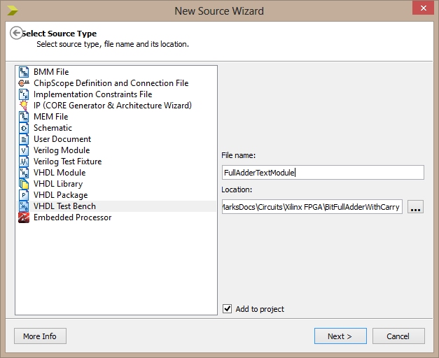
Once back in the Designer, add a new source module as before but this time select VHDL Test Bench for the source type.
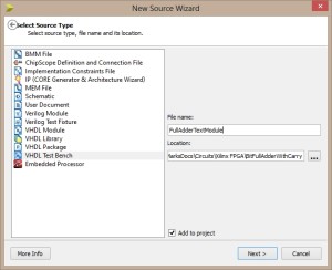
New Test Module
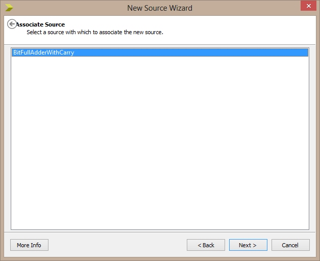
Next select the source file test test code will be associated with. We only have one file in our project so you must select that.

Associate With Source File
As with the previous cases, the next dialog in the wizard presents a summary for us to confirm the options we have selected.
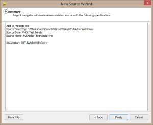
New Test Module Summary
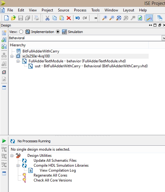
The Hierarchy will now show a new source file inserted between the device name and the source module we had previously created. This new file contains the test code for out module. The original code is also prefixed with uut which stands for Unit Under Test.
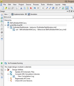
Project After Adding Test Module
Select the file containing the source code for the test module. This will have the default code for a test module.
--------------------------------------------------------------------------------
-- Company:
-- Engineer:
--
-- Create Date:   13:01:13 11/16/2013
-- Design Name:
-- Module Name:   BitFullAdderWithCarry/FullAdderTextModule.vhd
-- Project Name:  BitFullAdderWithCarry
-- Target Device:
-- Tool versions:
-- Description:
--
-- VHDL Test Bench Created by ISE for module: BitFullAdderWithCarry
--
-- Dependencies:
--
-- Revision:
-- Revision 0.01 - File Created
-- Additional Comments:
--
-- Notes:
-- This testbench has been automatically generated using types std_logic and
-- std_logic_vector for the ports of the unit under test.  Xilinx recommends
-- that these types always be used for the top-level I/O of a design in order
-- to guarantee that the testbench will bind correctly to the post-implementation
-- simulation model.
--------------------------------------------------------------------------------
LIBRARY ieee;
USE ieee.std_logic_1164.ALL;

-- Uncomment the following library declaration if using
-- arithmetic functions with Signed or Unsigned values
--USE ieee.numeric_std.ALL;

ENTITY FullAdderTextModule IS
END FullAdderTextModule;

ARCHITECTURE behavior OF FullAdderTextModule IS

    -- Component Declaration for the Unit Under Test (UUT)

    COMPONENT BitFullAdderWithCarry
    PORT(
         a : IN  std_logic;
         b : IN  std_logic;
         cin : IN  std_logic;
         result : OUT  std_logic;
         cout : OUT  std_logic
        );
    END COMPONENT;


   --Inputs
   signal a : std_logic := '0';
   signal b : std_logic := '0';
   signal cin : std_logic := '0';

 	--Outputs
   signal result : std_logic;
   signal cout : std_logic;
   -- No clocks detected in port list. Replace <clock> below with
   -- appropriate port name

   constant <clock>_period : time := 10 ns;

BEGIN

	-- Instantiate the Unit Under Test (UUT)
   uut: BitFullAdderWithCarry PORT MAP (
          a => a,
          b => b,
          cin => cin,
          result => result,
          cout => cout
        );

   -- Clock process definitions
   <clock>_process :process
   begin
		<clock> <= '0';
		wait for <clock>_period/2;
		<clock> <= '1';
		wait for <clock>_period/2;
   end process;


   -- Stimulus process
   stim_proc: process
   begin
      -- hold reset state for 100 ns.
      wait for 100 ns;

      wait for <clock>_period*10;

      -- insert stimulus here

      wait;
   end process;

END;
Remember I mentioned an issue I had with the consistency of the source code generated by the Designer. Check out the keywords in the test module and compare to the template source code for a module. Take the library keyword. In the template module code the keyword is in lower case. In the test module template it is upper case.
The test module contains the component definitions we require to test our module. Note that the module also contains a default clock for the circuits which need it. Editing the file above to remove unused items (and also correct the case to make it consistent with the source module).
--------------------------------------------------------------------------------
-- Company:
-- Engineer:
--
-- Create Date:   13:01:13 11/16/2013
-- Design Name:
-- Module Name:   BitFullAdderWithCarry/FullAdderTextModule.vhd
-- Project Name:  BitFullAdderWithCarry
-- Target Device:
-- Tool versions:
-- Description:
--
-- VHDL Test Bench Created by ISE for module: BitFullAdderWithCarry
--
-- Dependencies:
--
-- Revision:
-- Revision 0.01 - File Created
-- Additional Comments:
--
-- Notes:
-- This testbench has been automatically generated using types std_logic and
-- std_logic_vector for the ports of the unit under test.  Xilinx recommends
-- that these types always be used for the top-level I/O of a design in order
-- to guarantee that the testbench will bind correctly to the post-implementation
-- simulation model.
--------------------------------------------------------------------------------
library ieee;
use ieee.std_logic_1164.ALL;

entity FullAdderTextModule is
end FullAdderTextModule;

architecture behavior of FullAdderTextModule is
    --
    --  Component Declaration for the Unit Under Test (UUT)
    --
    component BitFullAdderWithCarry
    port (
         a : in  std_logic;
         b : in  std_logic;
         cin : in  std_logic;
         result : out  std_logic;
         cout : out  std_logic
        );
    end component;
    --
    --  Inputs
    --
    signal a : std_logic := '0';
    signal b : std_logic := '0';
    signal cin : std_logic := '0';
    --
 	--  Outputs
    --
    signal result : std_logic;
    signal cout : std_logic;
begin
    --
	-- Instantiate the Unit Under Test (UUT)
    --
    uut: BitFullAdderWithCarry port map
        (
            a => a,
            b => b,
            cin => cin,
            result => result,
            cout => cout
        );
    --
    --  Stimulus process
    --
    stim_proc: process
    begin
        -- hold reset state for 100 ns.
        wait for 100 ns;
        --
        --  0 + 1, carry in = 0
        --  Result should be 1 with no carry out.
        --
        a <= '0';
        b <= '1';
        cin <= '0';
        wait for 5 ns;
        --
        --  1 + 0, carry in = 0
        --  Result should be 1 with no carry out.
        --
        a <= '1';
        b <= '0';
        cin <= '0';
        wait for 5 ns;
        --
        --  1 + 1, carry in = 0
        --  Result should be 0 with carry out set to 1.
        --
        a <= '1';
        b <= '1';
        cin <= '0';
        wait for 5 ns;
        --
        --  0 + 1, carry in = 1
        --  Result should be 0 with carry out set to 1.
        --
        a <= '0';
        b <= '1';
        cin <= '1';
        wait for 5 ns;
        --
        --  1 + 1, carry in = 1
        --  Result should be 1 with carry out set to 1.
        --
        a <= '1';
        b <= '1';
        cin <= '1';
        wait;
   end process;
end;
The main work in the above code is performed in the stim_proc process. The first thing that happens is to pause. This 100ns pause is recommended by Xilinx to allow the system to stabilise after a reset.
The next code blocks set the input signals to known levels and then pause for 5ns. The pause allows us to examine the outputs in the simulator.
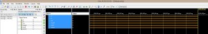
Now we have a test module we should re-run the simulator as before (right click on the Simulate Behavioral Module and select ReRun All). The simulator will launch again.

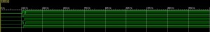
Simulated Full Adder Zoomed Out
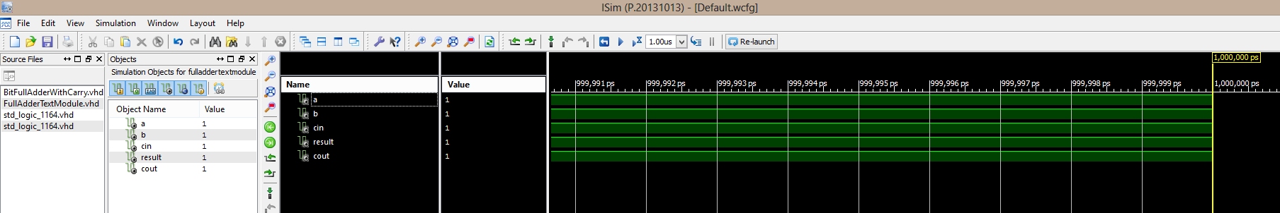
Notice that this time the traces to the right showing the signals are green and not brown. This is because the various ports have values assigned to them by the default test template. Previously there were no values assigned to the pins and they were undefined.
The default setting for the simulator is to run the simulation for 1us (1,000,000ps). The trace shows the final part of the simulation. Click on the Zoom to Full icon in the toolbar

to see the results of the fill run.
Full View of Trace
Looking at the far left of the trace you can see that all of the inputs are set to zero and the corresponding output levels are also zero. At 100ns the traces start to change as the test code changes the input values to the adder circuit.
Click on the zoom icon to zoom in on the traces. You can also use the scrollbar at the bottom of the trace to move around the output.
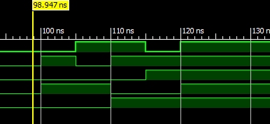
Zooming in until you can clearly see the signals between 100ns and 130ns shows the output from the test circuit generated by the code entered in the test module.
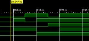
Zoomed In View Of Trace
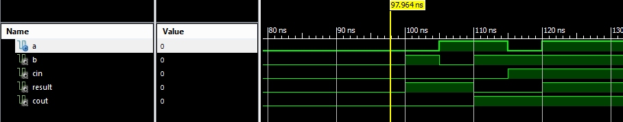
To the far left of the output window is a yellow cursor line. Grabbing this and dragging the cursor over the traces changes the values displayed for the various pins in the model. So just before 100ns into the simulation the output shows that all of the inputs are zero and so are the corresponding outputs:
97ns Into Simulation
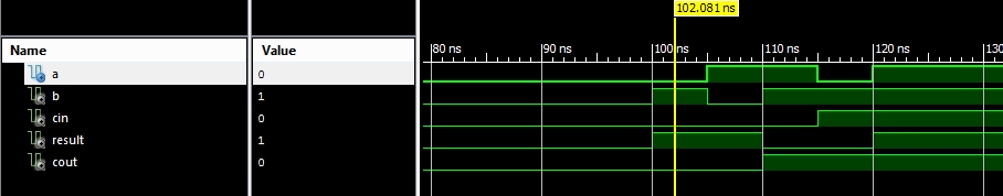
Moving the cursor through the simulation changes the values. So 102.081ns into the simulation we should have just completed execution of the following code:
--
--  0 + 1, carry in = 0
--  Result should be 1 with no carry out.
--
a <= '0';
b <= '1';
cin <= '0';
wait for 5 ns;
From the truth table presented at the start of this post we should be expecting result to be 1 and carry out to be 0. This is verified by the following output:

10ns Into Simulation
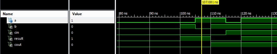
Similarly, at 107.081ns into the simulation we are executing the following code:
--
--  1 + 0, carry in = 0
--  Result should be 1 with no carry out.
--
a <= '1';
b <= '0';
cin <= '0';
wait for 5 ns;
Again, double checking with the truth table we see that we are expecting result to be 1 and carry out to be 0.
Once again the trace verifies this.
Deploying to the Board
This article was supposed to end with the deployment of the design to the Elektor FPGA board. The board has two LEDs which can be used for output and we can use jumper leads for the three inputs to the board.
Xilinx Software Problems
All was going well until I started to map the signals to the pins on the board using the Xilinx PlanAhead tool. At this point PlanAhead displayed the banner and then simply quit. The output in the console reported the fact that a log file had been generated. Opening the log file I found this:
****** PlanAhead v14.7 (64-bit)
  **** Build 321239 by xbuild on Fri Sep 27 19:29:51 MDT 2013
    ** Copyright 1986-1999, 2001-2013 Xilinx, Inc. All Rights Reserved.

INFO: [Common 17-78] Attempting to get a license: PlanAhead
INFO: [Common 17-290] Got license for PlanAhead
INFO: [Device 21-36] Loading parts and site information from C:/Xilinx/14.7/ISE_DS/PlanAhead/data/parts/arch.xml
Parsing RTL primitives file [C:/Xilinx/14.7/ISE_DS/PlanAhead/data/parts/xilinx/rtl/prims/rtl_prims.xml]
Finished parsing RTL primitives file [C:/Xilinx/14.7/ISE_DS/PlanAhead/data/parts/xilinx/rtl/prims/rtl_prims.xml]
start_gui
#
# A fatal error has been detected by the Java Runtime Environment:
#
#  EXCEPTION_ACCESS_VIOLATION (0xc0000005) at pc=0x000007fa87e21355, pid=64, tid=8124
#
# JRE version: 7.0_17-b02
# Java VM: Java HotSpot(TM) 64-Bit Server VM (23.7-b01 mixed mode windows-amd64 compressed oops)
# Problematic frame:
# C  [msvcrt.dll+0x1355]  free_dbg+0x5
#
# Failed to write core dump. Minidumps are not enabled by default on client versions of Windows
#
# An error report file with more information is saved as:
# E:\MarksDocs\Circuits\Xilinx FPGA\BitFullAdderWithCarry\hs_err_pid64.log
#
# If you would like to submit a bug report, please visit:
#   http://bugreport.sun.com/bugreport/crash.jsp
# The crash happened outside the Java Virtual Machine in native code.
# See problematic frame for where to report the bug.
#
Problems Solved
I have had the PlanAhead tool working in the past as I had completed the exercises in the Elektor magazines in the past. Time for some investigation. After several hours, and I do mean several hours, I uninstalled the 14.7 version of the tools and downloaded the 14.3 version from October 2012. Interestingly, this fixed the problem and PlanAhead launched as expected. So, on with the exercise.
On With the Exercise
The next step is to deploy the full-adder to the Elektor board connecting the ports to the pins on the board. We should be able to use jumper cables to represent the inputs to the full adder. The board contains two LEDs which we can use to show the output from the adder.
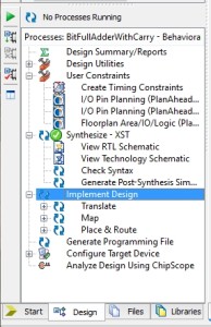
Firstly, we switch back to the Implementation view, expand Synthesise – XST and click on the green triangle to start the synthesis. This took a minute or so on my machine so expect to wait for the process to complete.
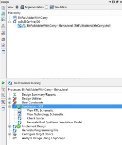
Getting Ready For Implementation
From the green tick in the processes panel above you can see that the synthesis completed with no errors.
The next step is to assign pins on the board to the input and output signals.
Double click on I/O Planning (PlanAhead) Post-Synthesis item in the User Constraints treeview. You will be presented with the following window:
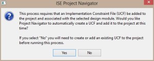
User Constraints File Question
Answer Yes to this question. After a while the PlanAhead tool should appear.
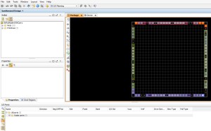
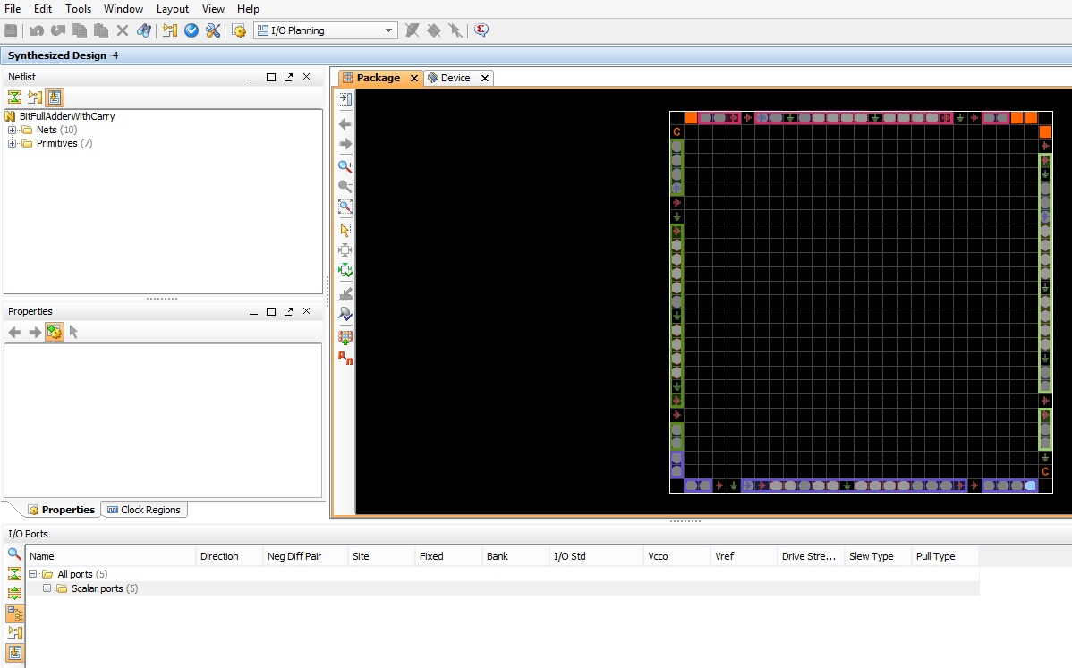
Plan Ahead Start Up
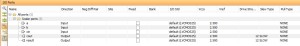
We now need to start assigning the pins on the board to the inputs/outputs in the design. So click on the Scalar Ports treeview item in the lower lefthand corner of the PlanAhead tool. PlanAhead will now show the inputs and outputs from the model.
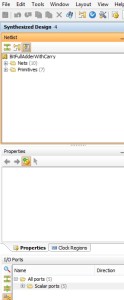
Plan Ahead Left Hand Panel
We can not start to assign the ports used in the model to the physical pins on the chip (and hence the board). The Elektor board has two LEDs which are connected to pins 90 and 91 of the FPGA. So for the two output rows set the entry in the Site column to 90 and 91. The entry in the I/O Std column should be set to LVCMOS33 for all of the pins.
IO Ports Expanded
Once the pins have been selected and assigned, save the mapping in the PlanAhead tool and return to the Designer. Select Implement Design and either right click and select Run or click on the green triangle. After a short time the system should indicate that the implementation has completed without error:
Implement Design
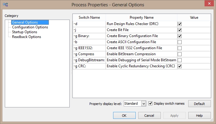
The final step is to generate the file which will be used by the FPGA. This is achieved by selecting Generate Programming File in the Designer, right clicking and selecting Process properties
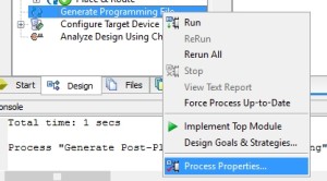
Process Properties
This will present the Process Properties dialog.
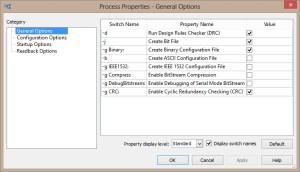
Process Properties Dialog
Ensure that the following options are checked in the Process Properties dialog:
| Category | Option | Value |
| General Options | Create Binary Configuration File | Tick this option |
| Configuration Options | Configuration Pin Program | Float |
| Configuration Options | Unused IOB Pins | Float |
| Startup Options | Drive Done Pin High | Tick this option |
Select OK and return to the Designer. You can now right click on the Generate Programming File entry in the Designer and select Run.
At the end of the process you will find a new file has been placed in the project directory, in this case bitfulladderwithcarry.bin.
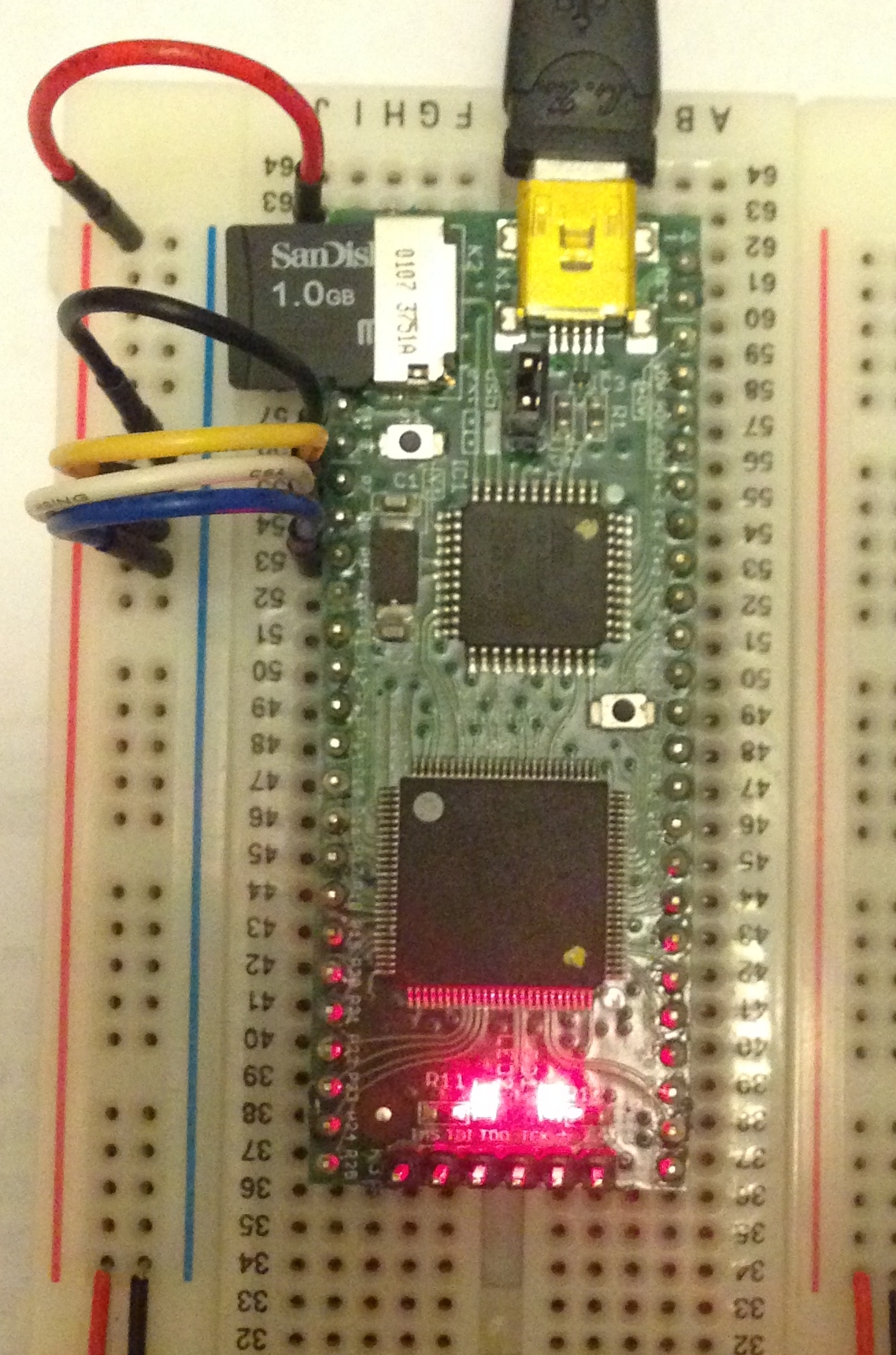
We are now ready to transfer the file to the FPGA board. According to the Elektor specs this is a simple process of connecting the board to the PC via USB and a new drive should appear in the file explorer. I must admit I have had intermittent success with this. I have found the most reliable way of transferring the file to the FPGA board is to insert the SD card into the PC and copy the bin file to the SD card. Once the file has been copied it must be renamed to config.bin. Next plug the SD card into the FPGA board and power the board (I used USB for this example).
Testing
In order to test the application you will need to power the board and then connect a,b and carry in to the appropriate signal levels and observe the LED output.
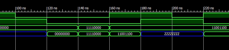
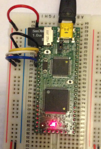
Grounding pins 7, 8 and 9 on the board should turn off both of the LEDs. In fact it turns both of the LEDs on.

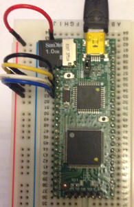
a=0,b=0,cin=0
Connecting all of the pins to a high signal should turn both LEDs on.
a=1,b=1,cin=1
As you can see, it turns the LEDs off. I looks like the signals are being interpreted in reverse (negated). Testing with a=0, b=0, cin=1 gives the following:
a=0,b=0,cin=1
The basic logic appears to be working although it is negated. A little more investigation is required.
Conclusion
It would have been nice to have completed the post with by deploying this to the FPGA board. Unfortunately to tools have let me down. Watch this space for future posts which will hopefully see this module deployed to the FPGA board.
The software swings between being amazing and buggy.
- The simulator is quick and easy to use although this comment comes from my novice perspective.
- The 64-bit editor quits every now and then when you try to copy text to the clip board. The 32-bit editor does not suffer from this problem.
- I have had a problem every now and then adding a new file to a project using the 64-bit Designer. Again, the 32-bit version of the tools do not have this problem.
- You cannot launch the simulator from the 32-bit tools. This works fine with the 64-bit tools.
This is the first step on the journey, a journey which I feel will take a while.
Update 17 Nov 2013
Version 14.7 of the software demonstrated the fact that new versions are not always better. In fact 14.7 proved to be a huge waste of time for me. I spent several hours trying to work out why PlanAhead didi not work only to revert back to version 14.3 of the software which looks to be working well.
Some future work:
- Create a more convenient pin diagram for the Elektor board.
- Follow up on the negated signals.
Work for another day I feel.