Oscilloscope Trace
Ohhhh no, not another post about the NE555 timer! I’m sorry to say, yes, this is another article (or two) about the NE555, how it works and some applications.
I blog for two main reasons:
- As an aide-memoire
- Hopefully others will find these posts useful
So this first post will cover the theory behind the operation of the NE555 using the astable circuit as an example.
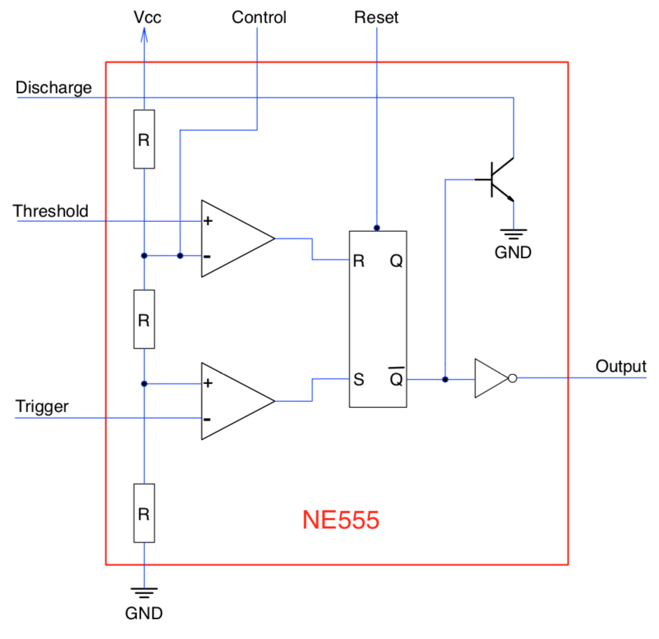
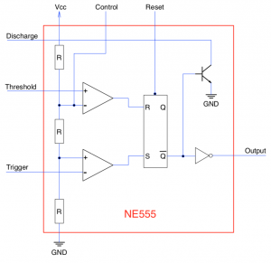
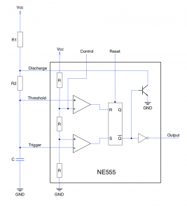
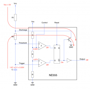
Logical Layout of the NE555
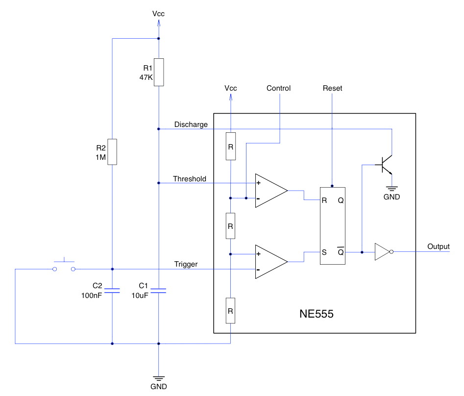
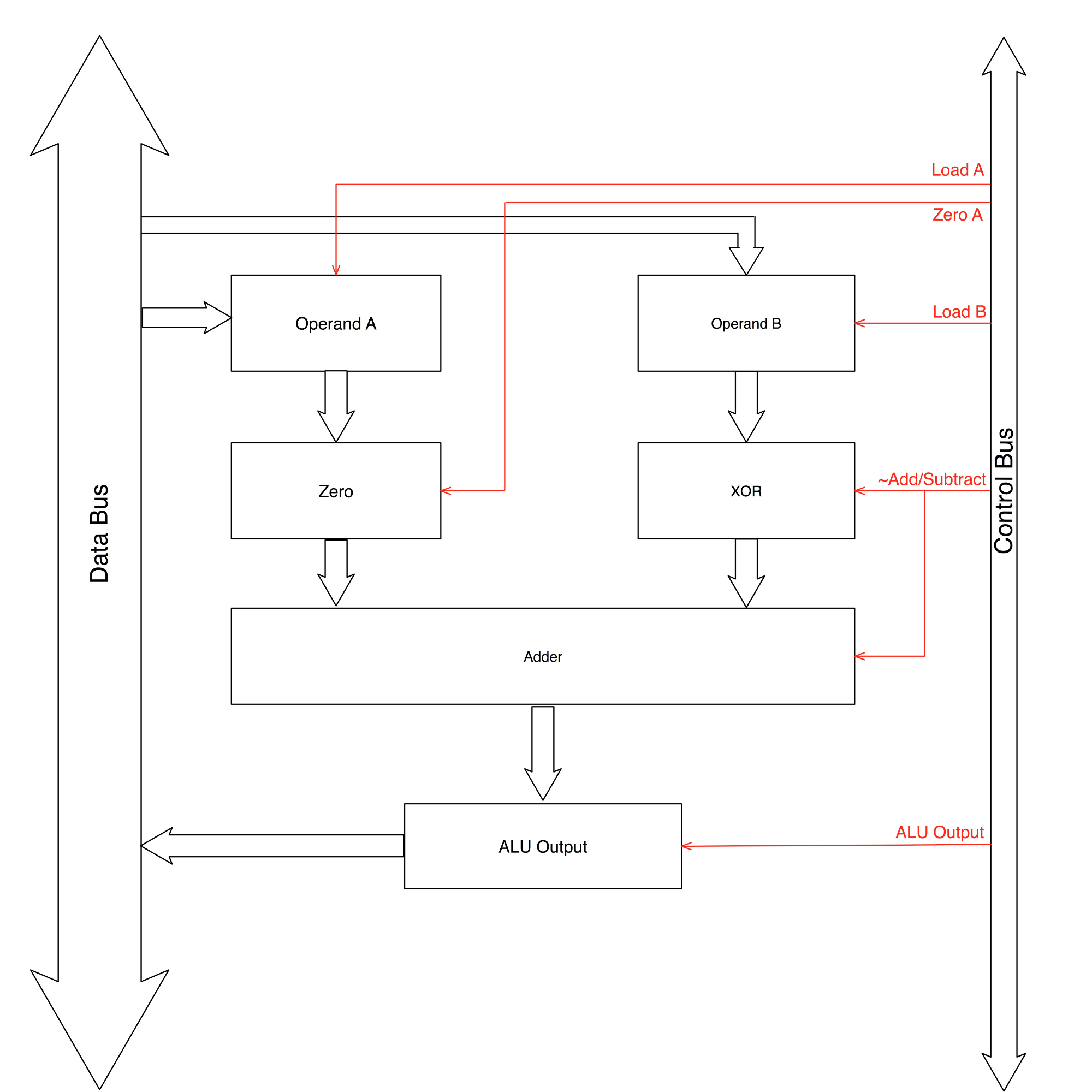
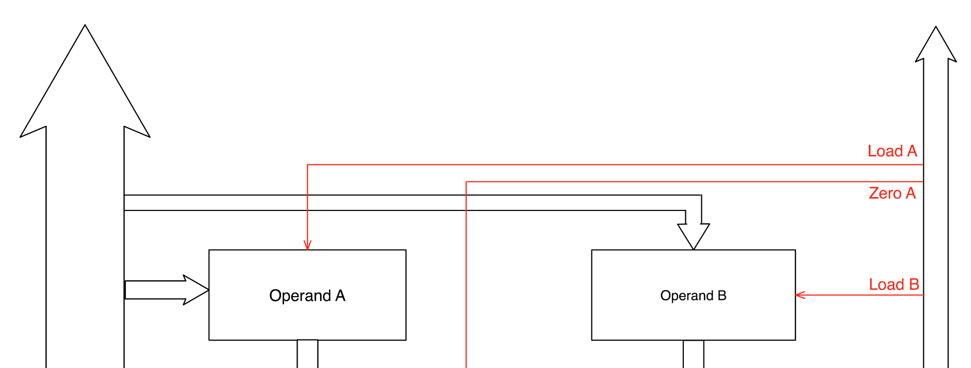
The NE555 has four logical units and they can be viewed logically in the following layout:
NE555 Logical Layout
These logical units are:
- Resistor ladder
- Two comparators
- S-R latch
- Discharge circuit
These components allow the engineering of a wide number of circuits using this versatile chip. This series of articles will cover four applications:
- Astable circuit (a.k.a a clock)
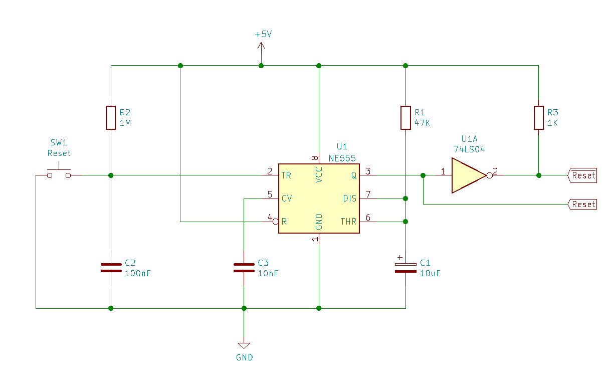
- Reset circuit
- Button debouncing a push switch
- Button debouncing with selection (i.e. latching switch)
Let’s start with looking at the four logical components identified above.
Resistor Ladder

Resistor Ladder
The resistor ladder in the original chip used 5K resistors. The use of three equal value resistors supply 1/3 * Vcc and 2/3 * Vcc to the two comparators.
Comparators
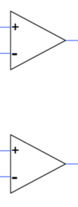
Comparators
The two comparators compare two of the input voltages to the two values from the resistor ladder, namely, 1/3 * Vcc and 2/3 * Vcc. They output a high value if the voltage on the positive input is greater than the voltage on the negative input.
The top comparator has the negative input connected to 2/3 * Vcc and the positive input connected to the threshold pin. This comparator will out a high value when the threshold is greater than 2/3 * Vcc and a low value at all other times.
The lower comparator has the negative input connected to 1/3 * Vcc and the positive input connected to the trigger input. This comparator will output a high value when the trigger is less than 1/3 * Vcc and a low value at all other times.
S-R Latch
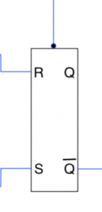
S-R Latch
The S-R latch uses the output from the two comparators to determine if the output of the NE555 should be turned on or off. The inverted output from the latch (Q) is connected to the output pin of the NE555 through an invertor.
Q is also connected to the base of the transistor connected to the discharge pin.
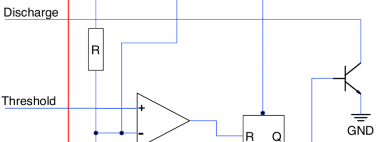
Discharge Circuit
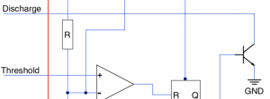
Discharge Circuit
The discharge pin is connected to ground through a transistor. The base of the transistor is connected to the inverted output of the S-R latch. So the discharge pin is connected to ground when the S-R latch is in the reset state.
So How Does it Work?
An astable circuit can be used to understand how the various components of the NE555 work together and it is this circuit we will examine next.
Astable Circuit
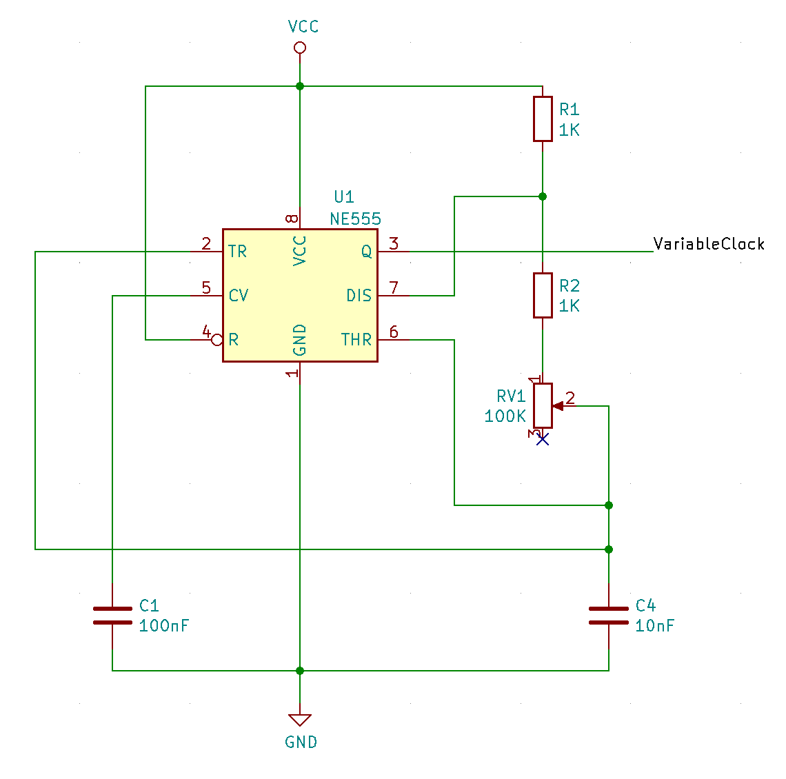
One of the circuits that can be constructed using the NE555 is a low frequency PWM circuit, known in NE555 parlance as an astable circuit. This can be used in a wide variety of applications from flashing LEDs to the provision of a low frequency clock signal for a digital circuit.
An simple astable circuit can be constructed using two resistors, a capacitor and the NE555 chip. Using the above logical diagram as a starting point we would connect the additional components as follows:
Astable Logical Layout
The reset pin should be connected to Vcc and the control pin should be connected to ground through a 100nF or 10nF capacitor.
The operation of the astable circuit will be consider by progressing through time from the point that power is applied to the circuit. It is assumed that Vcc is equal to 5V. The makes the nominal values for 1/3 * Vcc = 1.67V and 2/3 * Vcc = 3.3V.
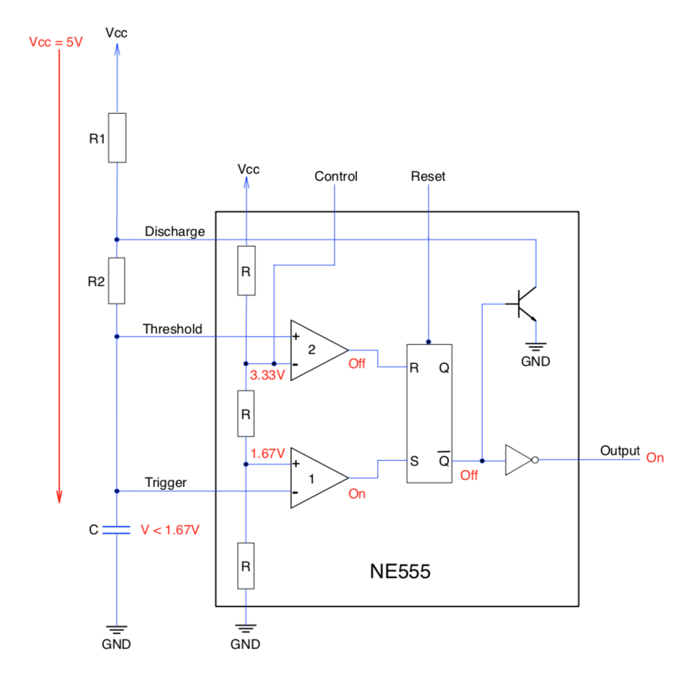
Power On
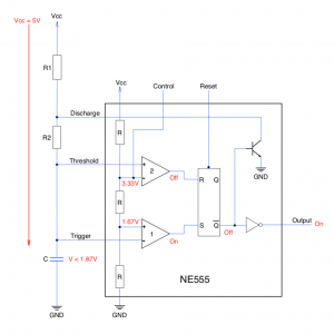
Capacitor starts to charge
At the point where the chip starts the resistor network inside the NE555 will split Vcc into two as noted above. These will appear on the two comparators negative (for comparator 1) and positive (for comparator 2) inputs.
At the same time, the capacitor C will be charged through resistors R1 and R2. At the point shortly after power up there will be very little charge on the capacitor, for argument, let us say that this is 0V. This will place 0V on both the trigger and threshold pins of the NE555.
Comparator 1 will compare the voltage on the trigger pin (negative input) to 1.67V (positive input). As 0V is less than 1.67V this will result in a high output from comparator 1. This high output is applied to the set pin of the S-R latch. Following this through, this will turn the Q output on and the inverted Q output off.
Q output drives both base of the transistor connected to the discharge pin, turning the transistor off and the output pin through the invertor, turning the output on.
Comparator 2 is comparing positive input connected to the charge on the capacitor (currently 0V) to 3.3V. Following this through as we did with comparator 1, 0V is not grester than 3.3V and so comparator 2 outputs a low signal. The low signal on the reset input in the S-R latch has no effect on the output from the S-R latch.
So shortly after power on, comparator 1 has turned the output of the NE555 on and capacitor C is charging. The various parts of the circuit have the inputs and outputs set to the values in the diagram above marked in red.
Capacitor Charge Reaches 1.67V
As time progresses, the charge on the capacitor will reach and then exceed 1.67V. The circuit will look like the following:
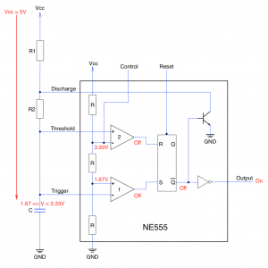
Capacitor continues to charge
At this point a change will occur to comparator 1. The negative input voltage (from the trigger pin) will reach 1.67V. The voltage on the negative input to the comparator will no longer be greater than 1.67V and so the output of the comparator will change from high (on) to low (off). The low signal applied to the set input of the S-R latch will have no effect on the S-R latch (both set and reset inputs to the S-R latch are now low and so the previous state is remembered).
At this point there is no change to the output of the circuit, the output is still latched on and charge continues to build up on the capacitor.
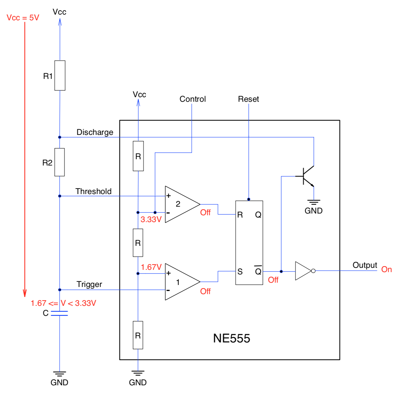
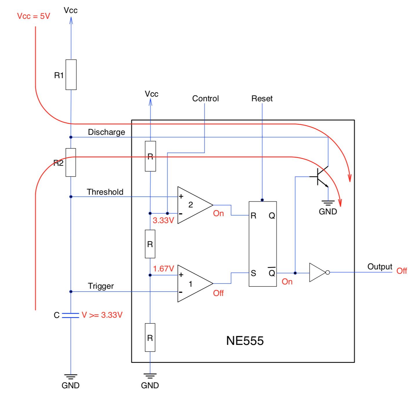
Capacitor Charge Reaches 3.33V
Eventually the charge on the capacitor will reach and exceed 3.33V. This will change the circuit to the following state:
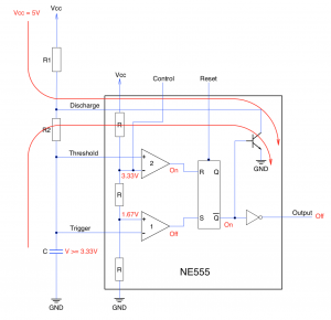
Capacitor starts to discharge
There will be no change to the output of comparator 1 as the voltage applied to the negative input of the comparator remains greater than 1.67V just as it was in the above stage.
The main change is triggered by comparator 2. The charge on the capacitor is applied to the positive input to the comparator which is now greater than or equal to the 3.33V (from the resistor ladder) applied to the negative input. This causes the comparator to set the output high.
A high output on comparator 2 is applied to the reset input of the S-R latch. This turns the set output (Q) of the latch off and the inverted output (Q) on.
Two things happen when Q is turned on:
- The output of the NE555 is turned off
- The transistor connected to the discharge pin is turned on
Turning the transistor on changes the flow of current through the circuit. So far current has been flowing through the two resistors, R1 and R2 to charge the capacitor, C. Now the current starts to flow from Vcc to ground through R1.
Current will now also start to flow from the capacitor, through R2 and the transistor to ground. At some point the charge on the capacitor will drop below 3.33V. This will be reflected on the threshold pin connected to comparator 2 and the output of this comparator will be turned off:
Middle of Capacitor Discharging
The output of the S-R latch will continue to hold the last state until and hence the output remains off until a signal is applied to the set pin of the S-R latch and so current continues to flow through the transistor.
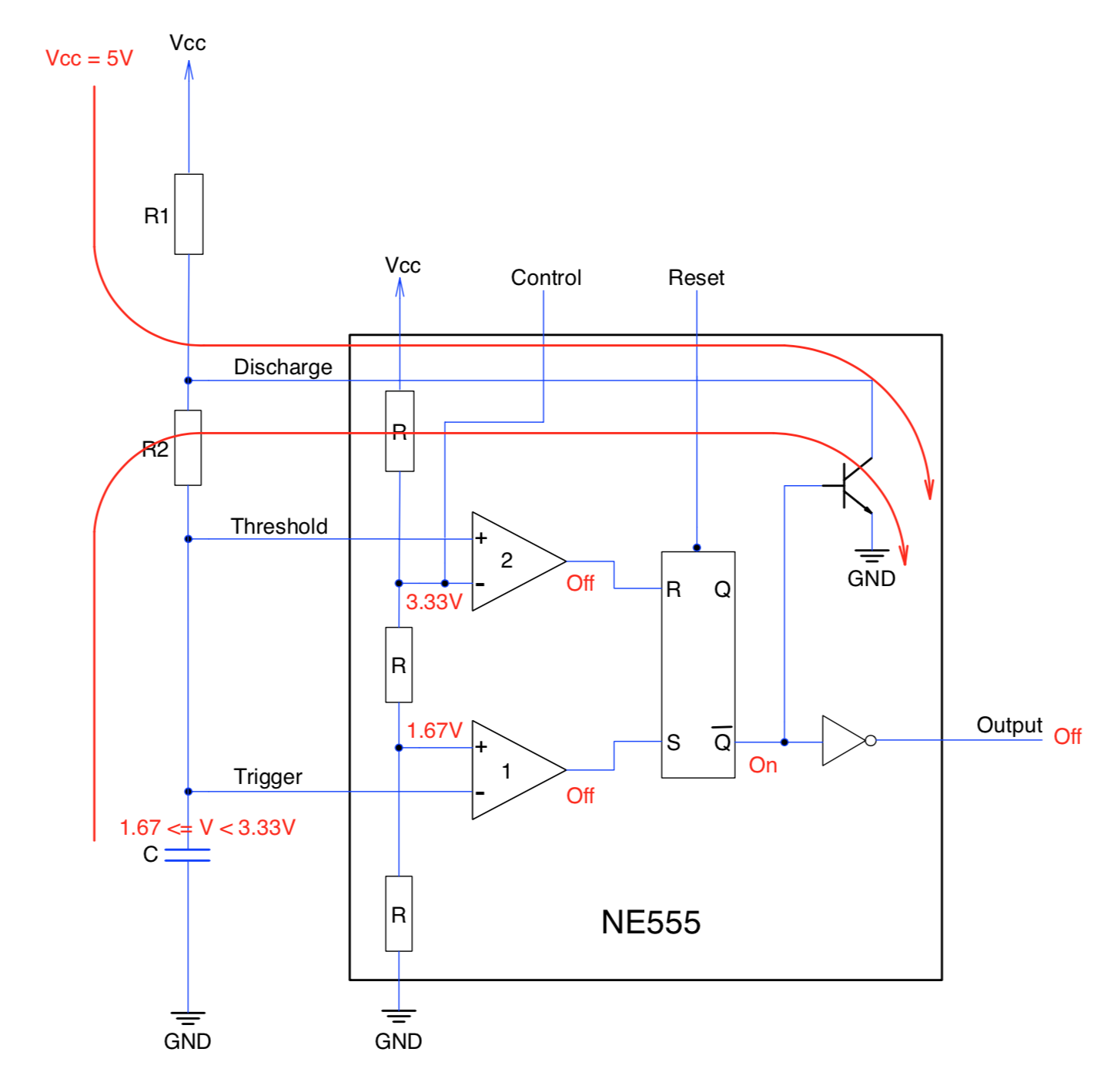
Capacitor Charge Drops Below 1.67V
At some point the charge on the capacitor will drop below 1.67V and comparator 1 turns on and so Q is turned off once more. The circuit starts to behave as though the system has just been powered on with one slight difference, the charge on the capacitor C starts at 1.67V instead of 0V. The whole cycle of charging and discharging repeats continuously.
Circuit Output
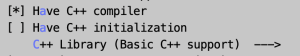
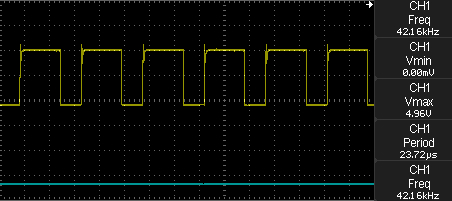
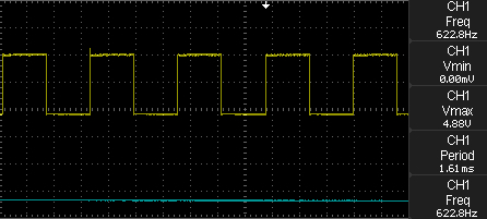
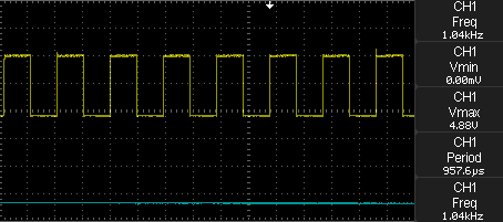
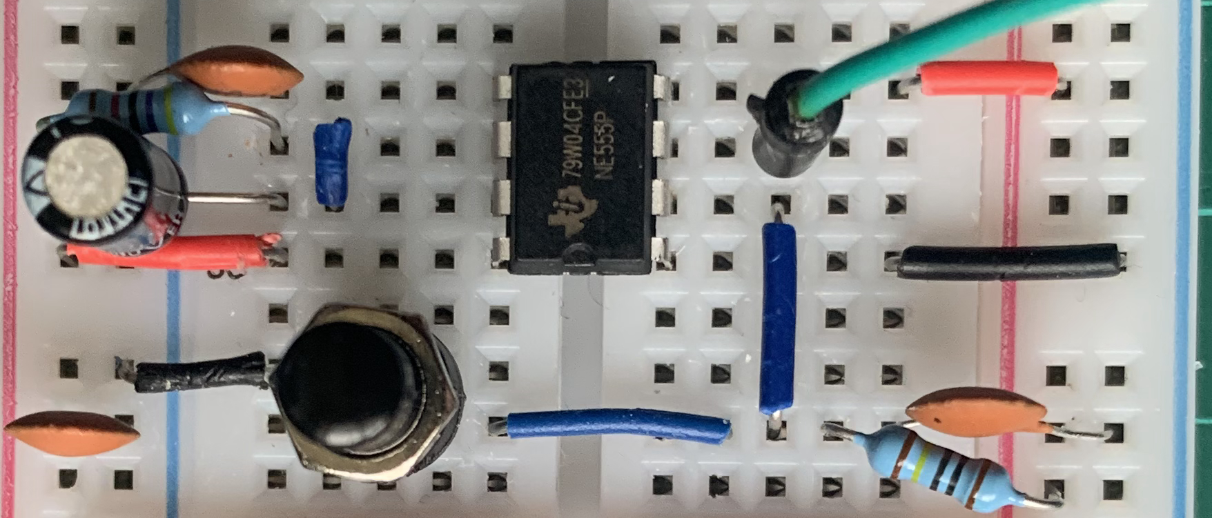
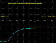
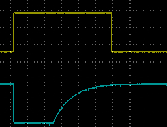
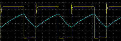
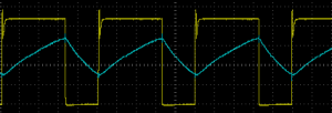
Building the circuit on breadboard and then connecting up an oscilloscope to the discharge and output pin shows the following trace:
Oscilloscope Trace
The output is shown in yellow and the discharge is shown in blue.
It is clear to see the charging and discharging of the capacitor coincides with the change in the output state of the NE555.
Timing Calculations
The timing calculations given in the data sheet for the NE555 are as follows.
Note that in the following calculations, resistance is expressed on Ohms, capacitance in Farads and time in seconds.
Charge Time
The charge time depends upon the capacitor and the two resistors R1 and R2 as current flows through the two resistors to charge the capacitor. The time taken to charge is given as:
tcharge = 0.693 * (R1 + R2) * C
Discharge Time
The discharge time is only dependent upon the capacitor and R2 as current does not flow through R1 when the circuit is discharging. the time take to discharge is given as:
tdischarge = 0.693 * R2 * C
Period
The period is the sum of the two timings tcharge and tdischarge. This can be expressed as:
Period = = 0.693 * (R1 + (2 * R2)) * C
The duty cycle and frequency are easily derived from the above.
And Finally…
The NE555 is a versatile chip that can act as more than a simple oscillator. The principles of the above circuit can be used in clock generation, switch debouncing, reset circuits and a whole range of other applications, several of which will be covered in following articles.
Dave Jones (EEVBlog) has put together the Three Fives Timer Kit and has videoed the build process and also provided a run down of the theory of operation referring to the kit schematic. Key times in the video are:
- 0 – 36 Minutes: Building the kit
- 36 – 54 Minutes: Examination of the schematic and run through the theory of operation
- 54 – 62 Minutes: Checking the voltages and output from the kit using an astable circuit