Using the Free Model Foundry 373 Latch Model
Saturday, December 28th, 2013The last post on VHDL/FPGA presented a naive implementation of a 74*373 latch and went as far as adding a little timing information to make the behavioural simulation a little more realistic. The post also hinted at the fact that there are some free VHDL libraries out on the net. This post uses a part from one of these libraries and shows how to add more accurate timing information to the behavioural simulation.
Free Model Foundry
The Free Model Foundry is an open source repository of VHDL and Verilog models. The models are freely available and the majority of the models are provided with timing information.
The 74xxxx series of chips can be located in the STD series of models. A quick check reveals that the library contains a 74*373 behavioural model in the file std373.vhd.
So let’s create a project and check out this model.
Creating a Project
First thing to do after starting Xilinx Webpack ISE is to create a new project to hold the circuit. From the startup screen select New Project:
ISE Project Navigator Start Up
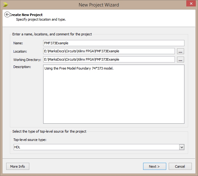
Now give the project a name. I selected FMF373Example, gave the project a short description and set the Top Level Source TYpe to HDL.
New Project Wizard Screen 01
Next set the device information:
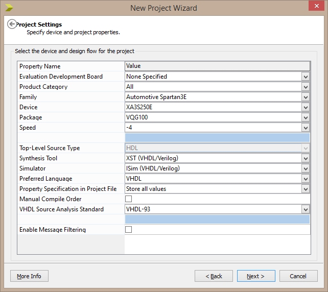
New Project Wizard Screen 02
The final window displays a summary of the project information:
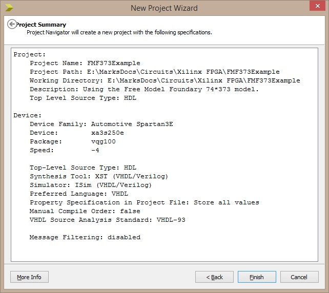
New Project Wizard Screen 03
The next step is to add the model to the empty project we have just created. Right click on the project and select Add Copy of Source…. Now navigate to the directory containing the VHDL source files for the FMF models and select the file std373.vhd. This will copy the file from the directory containing the original model files and place a new copy in the project directory.
Opening the source file for this model shows that the Free Model Foundry implementation is vastly more complex than the model presented in the previous post.
One of the first things to notice at the top of the file is that this model uses a number of libraries not seen in the previous posts, namely:
- IEEE.VITAL_timing
- IEEE.VITAL_primitives
- FMF.gen_utils
- FMF.ff_pacakge
The FMF libraries are supplied by the Free Model Foundry we simply need to add them to the project. Select the Libraries tab:
Libraries Tab
and add a New VHDL Library:
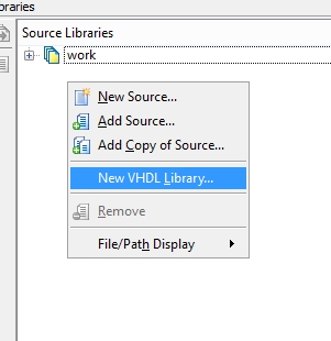
Add New Library
Name the library FMF and set the directory for the files to the location where the generic files are located on your machine:

FMF Library Properties
Next, add the files:

FMF Library Files
Next step, check that we can simulate the model we have so far. This will verify that all of the libraries are in place and the model compiles. Select Simulation and then open the simulator by right clicking on Simlate Behavioural Model and select run all. You should see something like the following:
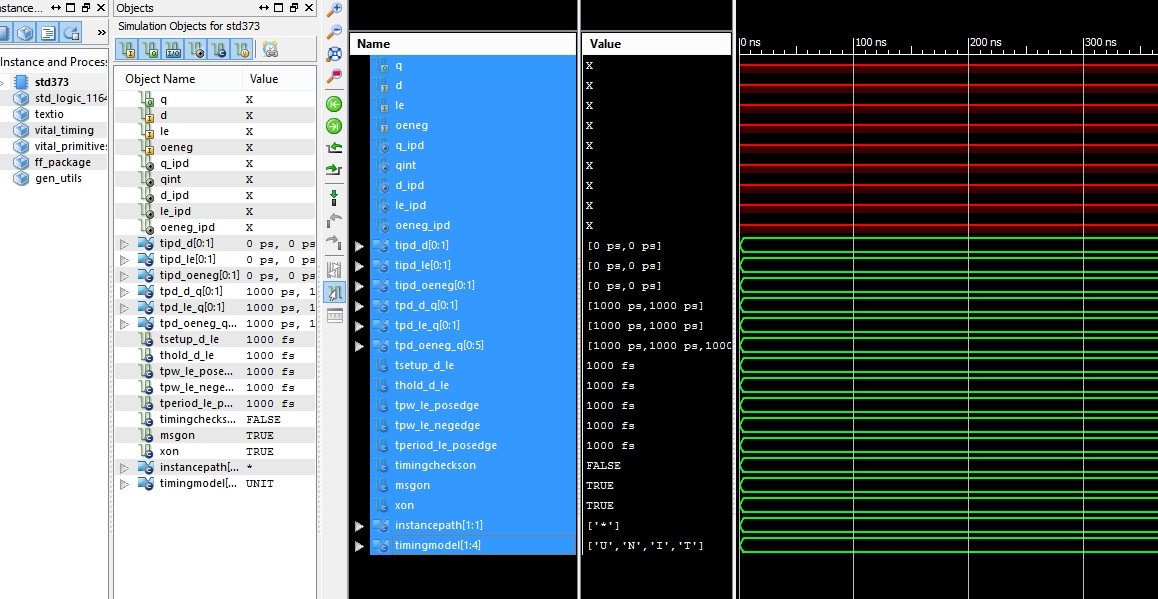
Simulation Run Without Test Bench
Close the simulator and return to the ISE Project Navigator.
Next step is to add a test bench. Follow the instructions in the previous post and add a new test bench. The system fails at this point with the message:
ERROR:HDLParsers:3014 – “E:/MarksDocs/Circuits/Xilinx FPGA/Library/Free Model Foundary/Generic Packages/gen_utils.vhd” Line 23. Library unit VITAL_primitives is not available in library IEEE.
To date I have still not been able to find a satisfactory answer to why this happens. Even Google is being of little help at the moment. To work around this I modified the code in the new test bench code window which was opened and created the following test bench:
LIBRARY ieee;
USE ieee.std_logic_1164.ALL;

-- Uncomment the following library declaration if using
-- arithmetic functions with Signed or Unsigned values
--USE ieee.numeric_std.ALL;

ENTITY LatchTest IS
END LatchTest;

ARCHITECTURE behavior OF LatchTest IS

    -- Component Declaration for the Unit Under Test (UUT)
    component std373
    port
    (
         LE : in  std_logic;
         OENeg : in  std_logic;
         D : in  std_logic;
         Q : out  std_logic
    );
    end component;

    --
    --  Inputs
    --
    signal le : std_logic := '1';
    signal oe : std_logic := '1';
    signal dataIn : std_logic := '0';
    --
 	--  Outputs
    --
    signal dataOut : std_logic;
    --
    --  Clock signal.
    --
    signal clock : std_logic := '0';
begin

	-- Instantiate the Unit Under Test (UUT)
    uut: std373 PORT MAP
    (
        LE => le,
        OENeg => oe,
        D => dataIn,
        Q => dataOut
    );

    --
    --  Provide an 8 MHz reference clock signal.
    --
    clockProcess: process
    begin
        clock <= '1';
        wait for 125 ns;
        clock <= '0';
        wait for 125 ns;
    end process;

    process
    begin
        --
        --  Initial condition, latch should have stabilised and be high impedance.
        --
        wait for 125 ns;

        le <= '0';
        wait for 125 ns;

        oe <= '0';
        wait for 125 ns;

        dataIn <= '1';
        wait for 125 ns;

        le <= '1';
        dataIn <= '1';
        wait for 125 ns;

        dataIn <= '0';
        wait for 125 ns;

        le <= '1';
        dataIn <= '1';
        wait for 125 ns;

        oe <= '1';
        wait for 125 ns;

        le <= '0';
        wait for 125 ns;

        le <= '1';
        oe <= '0';
        wait for 125 ns;
        --
        --  End of test.
        --
        wait;
    end process;
end;
Once entered, go back to the process window in the ISE Project Explorer, select Simulate Behavioural Model, right click and select ReRun All. The simulator windows should not open and show the following view when the global (full run) view has been selected:
Zoomed In Starting Simulation
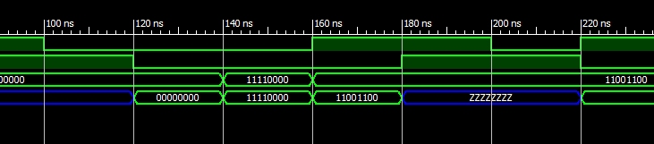
Now if we zoom in on the trace to the 250ns section of the simulation you can see that there is a 1ns gap between the OE line dropping from 1 to 0 and the data on the dataOut line changing from high impedance to 0:
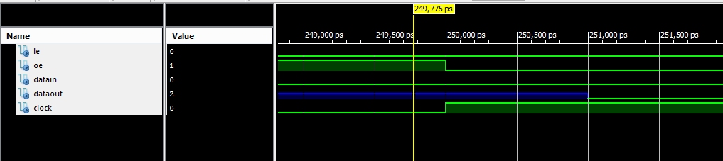
ZoomedIn At 250ns
We will now have a closer look at the code and examine why this happens.
STD373 – Transparent Latch
One of the first things to note about the STD373 implementation is that this file only contains a behavioural model for a single latch.
The 74*373 is actually an octal transparent latch where each latch has it’s own distinct data input and out put lines but all share a common latch enable and output enable line. eight of these latches are required in order to simulate a single 74*373 chip.
The second pint is that this file contains the abstracted behavioural model for a latch only. This does not include any additional implementation code for a synthesis-able model.
STD373 Entity Declaration
At the top of the std373.vhd file is the following code:
--------------------------------------------------------------------------------
-- ENTITY DECLARATION
--------------------------------------------------------------------------------
ENTITY std373 IS
    GENERIC (
        -- tipd delays: interconnect path delays
        tipd_D              : VitalDelayType01 := VitalZeroDelay01;
        tipd_LE             : VitalDelayType01 := VitalZeroDelay01;
        tipd_OENeg          : VitalDelayType01 := VitalZeroDelay01;
        -- tpd delays
        tpd_D_Q             : VitalDelayType01 := UnitDelay01;
        tpd_LE_Q            : VitalDelayType01 := UnitDelay01;
        tpd_OENeg_Q         : VitalDelayType01Z := UnitDelay01Z;
        -- tsetup values: setup times
        tsetup_D_LE         : VitalDelayType := UnitDelay;
        -- thold values: hold times
        thold_D_LE          : VitalDelayType := UnitDelay;
        -- tpw values: pulse widths
        tpw_LE_posedge      : VitalDelayType := UnitDelay;
        tpw_LE_negedge      : VitalDelayType := UnitDelay;
        -- tperiod_min: minimum clock period = 1/max freq
        tperiod_LE_posedge  : VitalDelayType := UnitDelay;
        -- generic control parameters
        TimingChecksOn      : Boolean  := DefaultTimingChecks;
        MsgOn               : BOOLEAN := DefaultMsgOn;
        XOn                 : Boolean  := DefaultXOn;
        InstancePath        : STRING   := DefaultInstancePath;
        -- For FMF SDF technology file usage
        TimingModel         : STRING   := DefaultTimingModel
    );
    PORT (
        Q       : OUT   std_logic := 'U';
        D       : IN    std_logic := 'X';
        LE      : IN    std_logic := 'X';
        OENeg   : IN    std_logic := 'X'
    );

    ATTRIBUTE VITAL_LEVEL0 of std373 : ENTITY IS TRUE;
END std373;
This declaration details the port specifications for the model along with the timing information.
Port Specification
The port specification tells us that this model has only three inputs and one output and that these are of type std_logic. This tells us that this is a single latch as all of the ports are single signals.
Timing Information
The upper section of the declaration contains the timing information. This information is used throughout the model and these values influence the timing of the signals in the simulation. Remember the 1 ns delay in the above trace. This comes from the UnitDelay01 delays set in this timing block.
A little digging around the internet lead me to the file timing_p.vhd (on my machine this was installed in the directory C:\Xilinx\14.3\ISE_DS\PlanAhead\scripts\rt\data\vhdl\pkgs). This file contains the types, attributes, constants and functions/procedures for the timing models. Opening this file gives the definitions for the types and constants used in the generic code block above. The top of the file looks like this:
TYPE VitalTransitionType IS ( tr01, tr10, tr0z, trz1, tr1z, trz0,
                              tr0X, trx1, tr1x, trx0, trxz, trzx);

SUBTYPE VitalDelayType     IS TIME;
TYPE VitalDelayType01   IS ARRAY (VitalTransitionType   RANGE tr01 to tr10)
     OF TIME;
TYPE VitalDelayType01Z  IS ARRAY (VitalTransitionType   RANGE tr01 to trz0)
     OF TIME;
TYPE VitalDelayType01ZX IS ARRAY (VitalTransitionType   RANGE tr01 to trzx)
     OF TIME;

TYPE VitalDelayArrayType     IS ARRAY (NATURAL RANGE <>) OF VitalDelayType;
TYPE VitalDelayArrayType01   IS ARRAY (NATURAL RANGE <>) OF VitalDelayType01;
TYPE VitalDelayArrayType01Z  IS ARRAY (NATURAL RANGE <>) OF VitalDelayType01Z;
TYPE VitalDelayArrayType01ZX IS ARRAY (NATURAL RANGE <>) OF VitalDelayType01ZX;
-- ----------------------------------------------------------------------
-- **********************************************************************
-- ----------------------------------------------------------------------

CONSTANT VitalZeroDelay     : VitalDelayType     :=   0 ns;
CONSTANT VitalZeroDelay01   : VitalDelayType01   := ( 0 ns, 0 ns );
CONSTANT VitalZeroDelay01Z  : VitalDelayType01Z  := ( OTHERS => 0 ns );
CONSTANT VitalZeroDelay01ZX : VitalDelayType01ZX := ( OTHERS => 0 ns );

---------------------------------------------------------------------------
-- examples of usage:
---------------------------------------------------------------------------
-- tpd_CLK_Q : VitalDelayType  := 5 ns;
-- tpd_CLK_Q : VitalDelayType01  := (tr01 => 2 ns, tr10 => 3 ns);
-- tpd_CLK_Q : VitalDelayType01Z := ( 1 ns, 2 ns, 3 ns, 4 ns, 5 ns, 6 ns );
-- tpd_CLK_Q : VitalDelayArrayType(0 to 1)
--                          := (0 => 5 ns, 1 => 6 ns);
-- tpd_CLK_Q : VitalDelayArrayType01(0 to 1)
--                          := (0 => (tr01 => 2 ns, tr10 => 3 ns),
--                              1 => (tr01 => 2 ns, tr10 => 3 ns));
-- tpd_CLK_Q : VitalDelayArrayType01Z(0 to 1)
--                        := (0 => ( 1 ns, 2 ns, 3 ns, 4 ns, 5 ns, 6 ns ),
--                            1 => ( 1 ns, 2 ns, 3 ns, 4 ns, 5 ns, 6 ns ));
---------------------------------------------------------------------------
The key to the problem for me was the comment block at the bottom of the block as this gives examples of how to use the types.
Setting The Timing Information
Some of the Free Model Foundry libraries contain timing information along with some tools detailing how the timing information can be used. At the moment I have been unable to work out how to use these tools and the timing information.
What I believe I have been able to do is to take the timing information in the data sheet for the 74HC373 and combine this with the model to adjust the behaviour of the code above. Here’s how I did it.
Looking at the VitalTransitionType there are eight types defined:
TYPE VitalTransitionType IS ( tr01, tr10, tr0z, trz1, tr1z, trz0,
                              tr0X, trx1, tr1x, trx0, trxz, trzx);
A little thought lead me to believe that the types are symbolic names for the transitions of the digital signals. So tr01 represents the transition from 0 to 1, tr0z represents a transition from 0 to high impedance etc.
Next we have the following code:
TYPE VitalDelayType01 IS ARRAY (VitalTransitionType RANGE tr01 to tr10) OF TIME;
This line of code defines a type containing two time elements. I believe that these represent the time delays for signals changing from 01 to 1 and also from 1 to 0.
If we combine this information with the following code from the entity definition of the std373 component:
-- tpd delays
tpd_D_Q             : VitalDelayType01 := UnitDelay01;
Here tpd_D_Q represents the time it takes for the input data (D) to be reflected on the output (Q). From the data sheet for the 74HC373 this is 18ns. Changing the above line to:
tpd_D_Q : VitalDelayType01 := (tr01 => 18 ns, tr10 => 18 ns);
Making a few more changes using the information in the data sheet gives the following timing code:
-- tipd delays: interconnect path delays
tipd_D              : VitalDelayType01 := VitalZeroDelay01;
tipd_LE             : VitalDelayType01 := VitalZeroDelay01;
tipd_OENeg          : VitalDelayType01 := VitalZeroDelay01;
-- tpd delays
tpd_D_Q             : VitalDelayType01 := (tr01 => 18 ns, tr10 => 18 ns);
tpd_LE_Q            : VitalDelayType01 := (tr01 => 30 ns, tr10 => 30 ns);
tpd_OENeg_Q         : VitalDelayType01Z := (tr01 => 12 ns, tr10 => 12 ns, tr0z => 12 ns, trz1 => 15 ns, tr1z => 9 ns, trz0 => 18 ns);
-- tsetup values: setup times
tsetup_D_LE         : VitalDelayType := 10 ns;
-- thold values: hold times
thold_D_LE          : VitalDelayType := 10 ns;
-- tpw values: pulse widths
tpw_LE_posedge      : VitalDelayType := 6 ns;
tpw_LE_negedge      : VitalDelayType := 7.3 ns;
-- tperiod_min: minimum clock period = 1/max freq
tperiod_LE_posedge  : VitalDelayType := 10 ns;
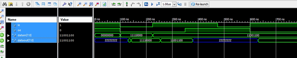
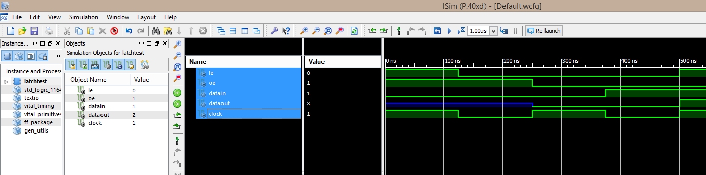
Running this through the simulator using the test bench gives the following trace:
Simulation With Added Timing Data
The trace shows that there is a delay between the data appearing on the data input and the same data appearing on the output pin. This appears to simulate the expected behaviour of a single latch using the timing parameters from the data sheet.
Conclusion
I am sure that there is a much better way to use timing information and further research is required into the simulation tools and the data from the models. The techniques presented here allow the use of the timing information from the data sheet in order to simulate the behaviour of the desired component.
This post was challenging to write as there is very little information easily available on the IEEE VITAL library. Even Google was of little help in this area. I have presented my understanding of the topic from the little information I was able to obtain. Looking at the results in the simulator it does appear that this technique is valid even if it is a little long winded. Hopefully I will find a way of using this information in a more efficient method once I am more familiar with the tools.
Next steps, combine eight of these to form a 74*373 latch and more research into the tools.