RSS

Archive for July, 2012

Configuring the STM8S System Clock – The Way of the Register

Sunday, July 29th, 2012

This post continues the low level use of the STM8S registers and shows you how to configure the STM8S system clock. In particular we will configure the system clock to use the internal high speed clock.

So let us start with a little background. The STM8S can be driven by three clock sources:

  • High Speed Internal (HSI) RC oscillator running at 16MHz
  • Low Speed Internal (LSI) RC oscillator running at 128KHz
  • External clock (1-24 MHz) which can be either an external crystal or user supplied clock.

We will be using the internal oscillator as this will be satisfactory for our purposes. An external clock may be more accurate but for most of the work I am doing I am happy to sacrifice the accuracy for the lower component count and greater simplicity of my designs.

At start up, the STM8S will be using HSI with a prescalar to bring the initial clock speed down to 2MHz. We will be resetting the clock prescalar to allow the chip to run at the full 16MHz.

The switching algorithm we will use is as follows:

  1. Reset all of the clock registers to the power on state
  2. Select the clock we wish to use
  3. Enable the switching mechanism
  4. Wait until the STM8S indicates that the clock has stabilised

Clock Registers

The description of the clock registers start around page 89 of the STM8S Reference Manual. In this article we will run through the registers concentrating on the values we will be setting. For a fuller description you should refer to the STM8S Reference Manual.

CLK_ICKR – Internal Clock Register

The only bits we will really be interested in for this example bits 1 and 0, this allows us to select the HSI and see if it is ready.

Register NameDescription
REGAHControl the actions of the internal voltage regulator when the chip enters Active-halt mode.
LSIRDYSet by hardware, this bit determines if the LSI is stabilised and ready. 0 indicates the oscillator is not ready, 1 indicates it is stable.
LSIENSet and cleared by the user program, this bit determines if the LSI has been selected as the clock source for the chip.
This can also be set by hardware to indicate that the LSI is required.
FHWUSet and cleared by the user program, this bit indicates if fast wakeup from Halt/Active -halt is enabled. 0 = disabled, 1 = enabled
HSIRDYSet and reset by hardware, this bit determines if the HSI is stable and ready for use.
HSIENSet and cleared by the user program, this bit determines if the HSI has been selected as the clock source for the chip.
This can also be set by hardware to indicate that the HSI is required.
0 indicates HSI is not selected, 1 indicates HSI is selected.

Our example here will be resetting the clock source on the STM8S chip to use the internal oscillator using HSIEN and using the HSIRDY bit to determine when the clock has been setup and is stable.

CLK_ECKR – External Clock Register

This register is used to provide information about the state of the external clock. We will not be using this register for anything other than resetting the register to the power on state.

Register NameDescription
HSERDYExternal high speed clock state, 0 = not ready, 1 = ready.
HSEENEnable/disable the external high speed clock. 1 = enabled, 0 = disabled

CLK_CMSR – Clock Master Status Register

This register is set and cleared by hardware and indicates which clock source is currently selected as the master clock source.

ValueClock Source
0xe1HSI
0xd2LSI
0xb4HSE

CLK_SWR – Clock Master Switch Register

This register is written to by the user program and is used to select the master clock source. The register cannot be written to whilst a clock source switch is on-going. You can test for the switch using the SWBSY in the CLK_SWCR register.

ValueClock Source Selected
0xe1HSI
0xd2LSI
0xb4HSE

Clock Switch Control Register – CLK_SWCR

The Clock Switch Control Register is used to control how and when the clock switch is performed.

Register NameDescription
SWBSYThis bit indicates if a clock switch is in progress, 1 = clock switch is on-going, 0 indicates that no switch is in progress.
This bit is set and cleared by hardware but can also be cleared in software. Clearing this bit resets the clock switch process.
SWENWriting a 1 into this bit starts the clock switching process.
SWIENEnable (1) or disable (0) an interrupt to be generated when a clock switch takes place.
SWIFIndicates if a clock switch is taking place (interrupts enabled) or is the target clock is ready (interrupts disabled)

In our case we will be using this register to start the clock switch process.

CLK_CKDIVR – Clock Divider Register

The system clock can be divided down to allow for lower clock frequencies to be used. This register allows for the HSI prescalar (divider) and the CPU prescalar to be set.

Register NameDescription
HSIDIVHSI prescalar
CPUDIVCPU Prescalar

The following values can be used for the HSI prescalar:

ValuePrescalar
0HSI frequency
1HSI frequency divided by 2
2HSI frequency divided by 4
3HSI frequency divided by 8

The following values are allowed for the CPU prescalar:

ValuePrescalar
0Master clock frequency
1Master clock frequency divided by 2
2Master clock frequency divided by 4
3Master clock frequency divided by 8
4Master clock frequency divided by 16
5Master clock frequency divided by 32
6Master clock frequency divided by 64
7Master clock frequency divided by 128

In this case we will want the CPU to be running at full speed and so no prescalars will be applied to either the master clock or the HSI.

CLK_PCKENR1 & CLK_ PCKENR2 – Peripheral Clock Gating Registers

These two registers enable (set to 1 and disable (set to 0) the clocks used to control the peripherals used in the application. I have fallen foul of these values a few times. If you set these registers or zero then you will turn off the peripheral clocks. This has the effect of turning off the feature you may be trying to use. If in doubt set both of these registers to 0xff. You can always refine the values later by restricting the clock signals to only those which you are using.

Register NamePeripheralDescription
CLK_PCKENR1TIM1Enable/disable timer 1
TIM3Enable/disable timer 2
TIM2/TIM5Enable/disable timer 2/5 (product dependent)
TIM4/TIM6Enable/disable timer 4/6 (product dependent)
UART1/2/3Enable/disable UART 1/2/3
SPIEnable/disable SPI
I2CEnable/disable I2C
CLK_PCKENR2CANEnable/disable the CAN bus
ADCEnable/.disable the analogue to digital converter
AWUEnable/disable the watchdog service

Enabling the service will use the frequency of the master clock. Disabling the clock to the service will turn it off.

The <iosstm8s103f3.h> file does not contain definitions for these bits, you need to define your own constants for these. I have recently taken to just turning them all on as I’m not too worried about the power requirements for the applications I am working on.

CLK_CSSR – Clock Security System Register

We will not be using this register in this example apart for setting the default power on value. Please see the STM8S Reference Manual for more information.

CLK_CCOR – Configurable Clock Output Register

We will not be using this register in this example apart for setting the default power on value. Please see the STM8S Reference Manual or future examples for more information.

CLK_HSITRIMR – HSI Clock Calibration Trimming Register

We will not be using this register in this example apart for setting the default power on value. Please see the STM8S Reference Manual for more information.

CLK_SWIMCCR – SWIM Clock Control Register

We will not be using this register in this example apart for setting the default power on value. Please see the STM8S Reference Manual for more information.

Software

As previously mentioned, this example will simply set the system clock to the maximum speed the HSI can deliver. We will then toggle a GPIO pin and hook this up to a scope to get an idea of the output. We will never see the full 16MHz clock speed of the HSI but we should be able to see that the output frequency changes when we change the clock dividers.

So first thing, let’s get the system set up and running at the full 16 MHz and see what we the scope produces.

#include <intrinsics.h>
#include <iostm8s103f3.h>

//
//  Setup the system clock to run at 16MHz using the internal oscillator.
//
void InitialiseSystemClock()
{
    CLK_ICKR = 0;                       //  Reset the Internal Clock Register.
    CLK_ICKR_HSIEN = 1;                 //  Enable the HSI.
    CLK_ECKR = 0;                       //  Disable the external clock.
    while (CLK_ICKR_HSIRDY == 0);       //  Wait for the HSI to be ready for use.
    CLK_CKDIVR = 0;                     //  Ensure the clocks are running at full speed.
    CLK_PCKENR1 = 0xff;                 //  Enable all peripheral clocks.
    CLK_PCKENR2 = 0xff;                 //  Ditto.
    CLK_CCOR = 0;                       //  Turn off CCO.
    CLK_HSITRIMR = 0;                   //  Turn off any HSIU trimming.
    CLK_SWIMCCR = 0;                    //  Set SWIM to run at clock / 2.
    CLK_SWR = 0xe1;                     //  Use HSI as the clock source.
    CLK_SWCR = 0;                       //  Reset the clock switch control register.
    CLK_SWCR_SWEN = 1;                  //  Enable switching.
    while (CLK_SWCR_SWBSY != 0);        //  Pause while the clock switch is busy.
}

//
//  Main program loop.
//
int main(void)
{
    __disable_interrupt();
    //
    //  Initialise Port D.
    //
    PD_ODR = 0;             //  All pins are turned off.
    PD_DDR_DDR4 = 1;        //  Port D, bit 4 is output.
    PD_CR1_C14 = 1;         //  Pin is set to Push-Pull mode.
    PD_CR2_C24 = 1;         //  Pin can run up to 10 MHz.
    //
    //  Now setup the system clock
    //
    InitialiseSystemClock();
    __enable_interrupt();
    while (1)
    {
        PD_ODR_ODR4 = 1;    // Turn Port D, Pin 4 on.
        PD_ODR_ODR4 = 0;    // Turn Port D, Pin 4 off.
    }
}

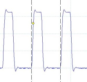
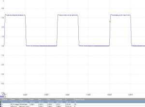
Running this code resulted in the following trace on the oscilloscope:

GPIO Output when the System Clock is set to HSI with no Divider.

GPIO Output when the System Clock is set to HSI with no Divider.

The frequency of the out was 2.693Mhz.

So now let’s see what happens when we set the prescalar for HSI to be 2 (i.e. half the clock speed. To do this we need to edit the code slightly, so change this:

CLK_CKDIVR = 0;                     //  Ensure the clocks are running at full speed.

to this:

CLK_CKDIVR = 0;                     //  Ensure the clocks are running at full speed.
CLK_CKDIVR_HSIDEV = 1;				//	Set the HSI divider to 2.

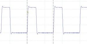
The result is the following trace:

GPIO Output when System Clock is set to HSI divided by 2

GPIO Output when System Clock is set to HSI divided by 2

This looks remarkably like the trace above but the oscilloscope shows that the frequency of the signal is now 1.335MHz, or approximately half of the frequency of the first trace.

The full project for this article can be downloaded from here. This code has been tested with my reference platform, the Variable Labs Protomodule and the STM8S Discovery board.

Compatibility

SystemCompatible?
STM8S103F3 (Breadboard)
Variable Lab Protomodule
STM8S Discovery

Komodex Seven Segment Display and Breakout Modules

Friday, July 27th, 2012

Komodex Labs recently released a couple of new modules for the Netduino GO! platform. The first is a seven segment display module and as we will see later this can be used to show sensor data. The second module is a breakout module for the GO! bus and this is probably more interesting to module developers.

As the postman was kind to me and managed to get these modules to me this week I thought I’d hook them up to the light sensor I have been playing with to see what they can do.

A Little Background

I have recently been working with a simple sensor to teach myself how to work with the STM8S. It has been a long slow task as the normal competing pressures of work, the house and general life stuff keeps calling for my attention.

The project uses a TSL235R sensor which converts the current ambient light level into a square wave with 50% duty cycle. The STM8S periodically reads the frequency of the signal generated by the sensor. This value is then made available to the Netduino GO! via the GO! Bus.

This project is going to read the value from the STM8S and display it on the seven segment display. The value is a 16-bit value and so can range from 0 to 65535 so we will be showing the value in hex.

Seven Segment Module

The seven segment display is a nice little module very professionally finished. It feels a solid – sort of odd to say that about a module. I was kind of surprised by the weight but then I have only been working with small modules so far.

I’d write more but I think the module is best described my Matt’s blog post. This shows some photos of the module along with a description of the API used to control it.

GO! Bus Breakout Module

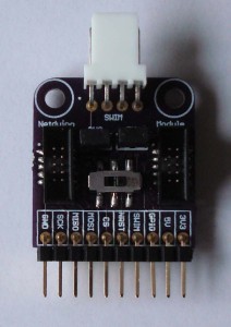
This is a handy little module which only had a short production run. I was lucky enough to have ordered one before stock ran out. The module is aimed at module developers. It has a couple of sockets for module cables along with some handy breakout points.

Komodex Labs GO! Bus Breakout Module

Komodex Labs GO! Bus Breakout Module

The idea is simple, you connect your Netduino GO! to one side of the breakout board and your module to the other side of the breakout board. You can then hook up test equipment (scope / logic analyser etc.) to a row of headers on the board. This allows you to debug your module by snooping on the data going down the GO! Bus.

An alternative configuration and one I am using for development on breadboard, is to connect the breakout module to breadboard with the Netduino GO! connected to one side of the breakout board. This allows you to feed the GO! Bus signals into your circuit whilst at the prototype stage.

The breakout also has a lovely feature in that you can connect the ST-LInk/V2 module to the board and at the flick of a switch you can disconnect the SWIM/NRST signals from the Netduino GO! and connect them to the ST-Link/V2 instead. This allows you to re-program the STM8S on the fly without having to modify your circuit – NEAT !

For more information about this module I’d head over to Matt’s blog post.

Hooking it all up

Connecting the Seven Digit Module up to the go was easy, it simply needed a standard 5cm GO! Bus cable and that’s it.

The Breakout module was a little more difficult as it had to be hooked into an existing prototype circuit. From the Netduino side it was easy, just another 5cm GO! Bus cable. The ST-Link/V2 connection was also easy as the module has a connector already on the board and it is designed to ensure that the connection can only be made one way. The only complication was then ensuring that the connections between the GO! Bus and the prototype circuit were correct. Adding this module has in fact made my prototype circuit a little cleaner.

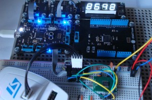
Here’s what the final circuit looks like:

Komodex Seven Segment in Light Sensor Prototype Circuit

Komodex Seven Segment in Light Sensor Prototype Circuit

Installing the Drivers

The Seven Segment Module is supplied with a set of drivers in the form of an executable. The drivers can be found on the Komodex Labs web site. Installation was quick, simple and painless.

Komodex Labs also provide the source code for the drivers along with a sample application. This is a separate download and as you will see later, this came in handy.

As you would expect, the breakout module does not require any drivers as there is no interaction between the module and the PC.

Writing the Software

The API provided with the module is comprehensive but in this case we are going to use only a small part of it. We need to display a hex representation of a 16-bit number.

So the first step is to create a new project and add a reference to the module. You will have to browse to the directory in which you installed the drivers and add the Komodex.NETMF.SevenSegmentDisplay.dll file. On my machine this was installed in C:Program Files (x86)KomodexModule DriversAssembliesv4.2

The next step is to add a using statement

using Komodex.NETMF;

and then declare and instantiate an instance of the module:

SevenSegmentDisplay display = new SevenSegmentDisplay();
display.SetValue(0);

The above shows the module being instantiated and the display value set to 0.

The remainder of the program continuously polls the sensor for a reading. This reading is converted into a string containing the hexadecimal representation of the reading. This reading is then displayed on the Seven Segment Module. The code looks something like this:

while (true)
{
	short diff = module.GetReading();
	string output = "";
	char c;
	for (int index = 3; index >= 0; index--)
	{
		int nibble = (diff >> (4 * index)) & 0xF;
		if (nibble < 10)
		{
			output += nibble.ToString();
		}
		else
		{
			c = (char) ('A' + nibble - 10);
			output += c.ToString();
		}
	}
	display.SetValue(output);
	Thread.Sleep(1000);
}

The line short diff = module.GetReading(); obtains a reading from the sensor module which I am prototyping. This value could come from any sensor or from any source / calculation.

Hitting F5 deployed the code to the Netduino GO! and values quickly started appearing on the display. Success!

No… Wait…

I’m getting some unexpected output. Every now and then the module displays a number with some spaces in place of digits. Hmmmmm… what is going on!

Time for a quick test program. I know that the module works OK as the test projects ran fine. Adding a Debug.Print of the output variable gave me a clue. There was a pattern. Any numbers with the digit 9 in them showed a space instead of a digit. A quick test program showed that displaying 2929 where the variable of type int displayed the number correctly. Doing the same where the value was stored in a string showed any digit except the digit 9, these were replaced with spaces. Now we know where the problem is.

As noted earlier, Komodex Labs supply the source code for the drivers. So opening this project and some poking around the code for the display resulted in the problem being found. A quick modification to the source, recompile and then reference the newly compiled DLL in my code and Success !

Edit: Komodex labs have confirmed that the driver has been patched and as of 27/07/2012 the driver download contains the fix for the problem noted.

Here is a short video of the sensor and display working together:

Simple GPIO – The Way of the Register

Sunday, July 8th, 2012

If you have been following this blog for a while you will be aware that I have recently changed the way I write code for the STM8S from using the STD Peripheral Library to using direct register access. This has required that I go back to basics learning a new way to perform tasks I had only just mastered. The Way of the Register posts will show you have to control the STM8 using register access.

This first post will look at a simple task, controlling GPIO lines. The aim of this first exercise is to simply toggle one of the GPIO lines.

Hardware

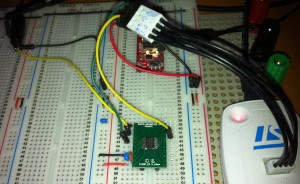
For this task we need very little hardware, only the STM8S set up on breadboard. For this we need a minimum of two capacitors and the chip itself. A 1uF capacitor is placed between VSS and VCAP and a 100 nF capacitor is placed between VDD and VSS. An additional 1uF capacitor is also placed across the +3.3V and ground of the power supply. The following shows this set up on breadboard along with the breadboard power supply, connections to the oscilloscope and the ST-Link programmer:

STM8S103 set up on Breadboard

STM8S103 set up on Breadboard

The Registers

Before we can start coding we need to have a look at the registers we will be using. The GPIO pins have five registers used to control the GPIO function and set/read the value of a pin. These are:

Register
Data Direction Register
Control Register 1
Control Register 2
Output Data Register
Input Data Register

The following sections provide a brief description of the registers. For more information you should consult RM0016 – STM8S Reference Manual.

Px_DDR – Data Direction Register

This register determines which or the GPIO pins are outputs and which are inputs. A value of one in a bit sets a port line to output and zero sets the port line to input. You can set the value of the whole register or each individual bit in the register.

To set the whole register in one go you would execute something like the following:

PD_DDR = 0x0f;

This sets bits 0-3 inclusive of port D to output whilst bit 4-7 are inputs.

An alternative to this is to set up each GPIO pin individually, so the equivalent of the above is:

PD_ODR = 0;
PD_DDR_DDR0 = 1;
PD_DDR_DDR1 = 1;
PD_DDR_DDR2 = 1;
PD_DDR_DDR3 = 1;

Px_CR1 & PxCR2 – Control Register 1 and 2

These two registers determine the properties of the pins depending upon the operating mode of the pin. The following table summarises the operating modes:

RegisterModeValueDescription
CR1Input0Floating input
CR1Input1Input with pull-up
CR1Output0Open drain
CR1Output1Push-Pull
CR2Input0Interrupt disabled
CR2Input1Interrupt enabled
CR2Output0Output up to 2 MHz.
CR2Output1Output up to 10 MHz

In our case, we need the output pin to operate in Push-Pull mode and as we do not know the final speed of the output signal we will set this to the maximum, 10 MHz.

As with the data direction register, each bit in the registers maps to a specific GPIO on each port. In the case of these registers the bits are labelled C10-C17 (for Control Register 1) and C20-C27 (for control Register 2). The format appears to be CRB, where C stands for Control Register; R is an integer representing the register number and B is an integer representing the bit to be set.

In our case, this results in the following code:

PD_CR1_C14 = 1;
PD_CR2_C24 = 1;

Px_ODR – Input/Output Data Registers

These two registers allow you to read the value of an input pin and set the value of an output pin. As with the previous registers you can set/read the register in its entirety or bit by bit. So to turn all of the outputs off you would execute something like:

PD_ODR = 0;


In the case we have been using we will be outputting data on pin 4 of port D. So to set the pin high you would execute the following statement:

PD_ODR_ODR4 = 1;

Software

Now we have the theory in place lets put together a simple application which uses it. The following code sets up port D to have pin 4 configured as an output operating to 10 MHz. The main program loop then simply keeps flipping the bit. The result should be a square wave signal.

#include <iostm8S103f3.h>

int main( void )
{
    //
    //  Initialise Port D.
    //
    PD_ODR = 0;             //  All pins are turned off.
    PD_DDR_DDR4 = 1;        //  Port D, bit 4 is output.
    PD_CR1_C14 = 1;         //  Pin is set to Push-Pull mode.
    PD_CR2_C24 = 1;         //  Pin can run upto 10 MHz.
    //
    //  Now lets toggle to IO line.
    //
    while (1)
    {
        PD_ODR_ODR4 = 1;    // Turn Port D, Pin 4 on.
        PD_ODR_ODR4 = 0;    // Turn Port D, Pin 4 off.
    }
}

If we hook an oscilloscope up to PD4 on the STM8 chip we see the following:

Simple GPIO Output

Simple GPIO Output

As you can see, we have a square wave. Note that the wave is not symmetrical. This is due to the branch instruction being executed in the while loop to go back to the start of the loop.

Source Code

Here is the IAR project and source code for this post. This code has been tested on my reference platform, Variable Lab Protomodule and the STM8S Discovery board.

Compatibility

SystemCompatible?
STM8S103F3 (Breadboard)
Variable Lab Protomodule
STM8S Discovery