RSS

Archive for April, 2013

Making a Netduino GO! Module – Stage 5 – Enhancing the Drivers

Saturday, April 27th, 2013

This series of posts follows the steps required in order to make your own Netduino GO! module. To do this we are using a simple idea, an Output Expander (yes, it seems to have a name now) for the Netduino GO!. Using only a hand full of simple components, the Output Expander will add 32 digital outputs to the Netduino Go!.

The Story So Far…

The module has so far completed the following steps:

  • Concept and prototype on breadboard
  • Basic drivers
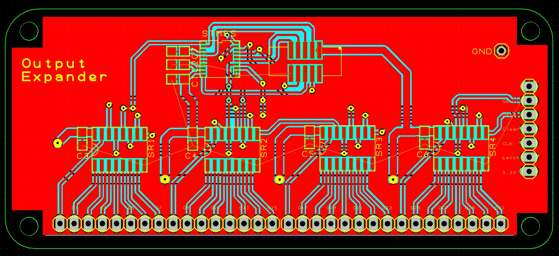
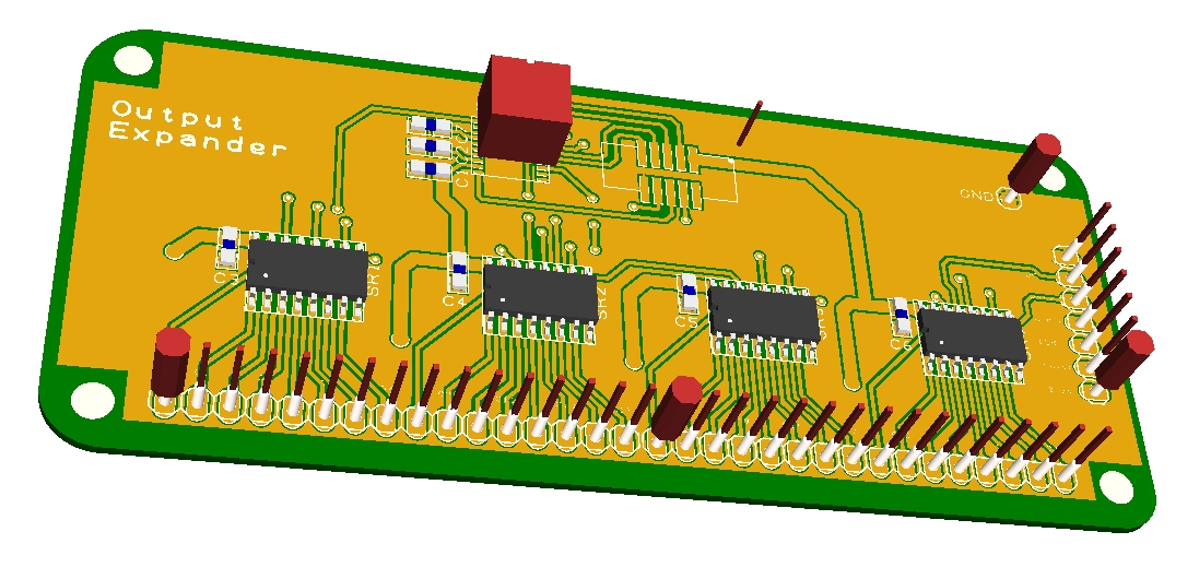
  • PCB design and layout
  • Generation of PCB manufacturing files

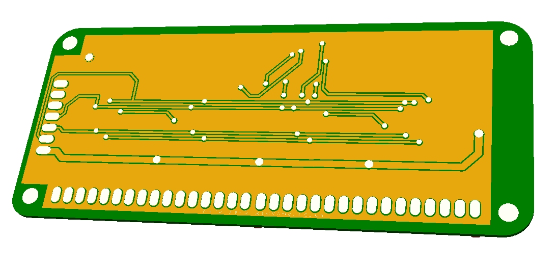
The first batch of 10 boards were ordered on 20th April 2013 using iTeads prototyping service. I am expecting the manufacturing process to take about one week with a further two weeks for shipping as I used the cheap, slow courier service.

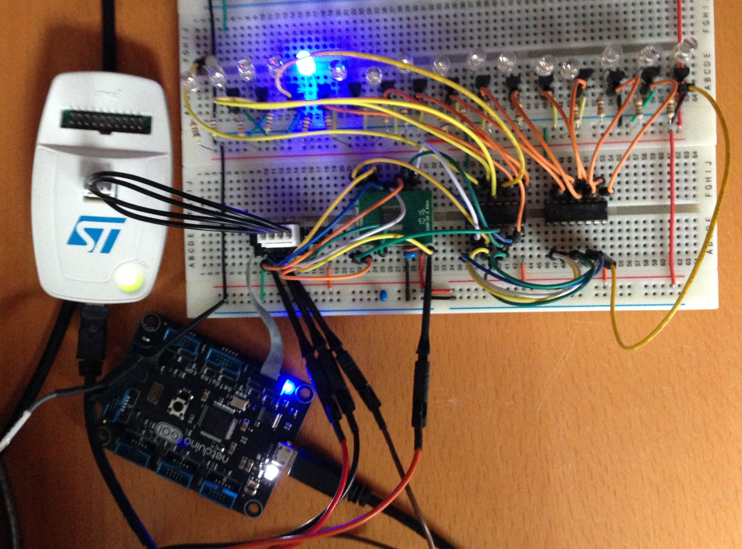
In the meantime we still have the breadboard prototype to work with. This may only have two shift registers attached to it but by carefully parametrising the code we should be able to develop a driver which only needs to be recompiled when the final hardware becomes available.

Features

The driver for this module should be relatively simple as we are merely setting outputs from the shift registers to be either on or off. We shall start with the following list of desired features:

  • Default initialisation to set up for one board
  • Set the bytes for the digital outputs
  • Array like access for the bits
  • Configurable latching mode (automatic or manual)
  • Clear the output
  • Turn outputs from the registers on or off

The only remaining task is to decide where the features are to be implemented. We have two options:

  • On the Netduino GO! in C#
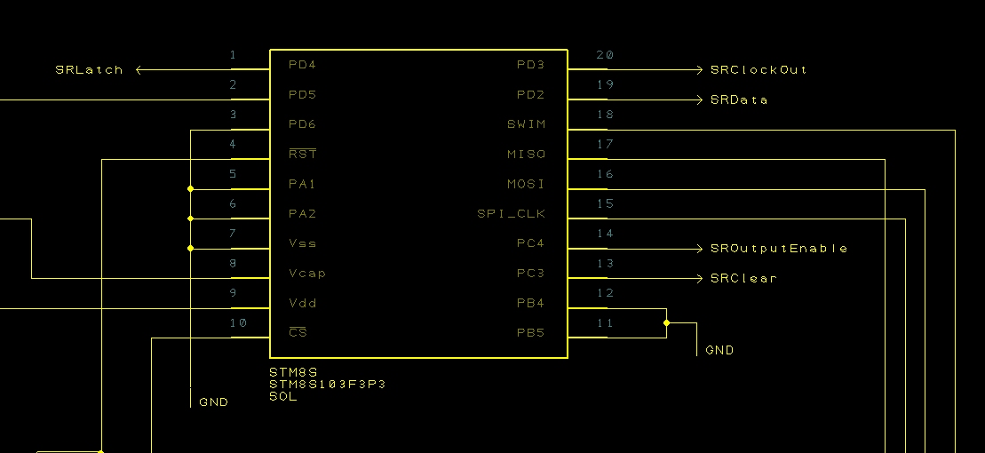
  • On the STM8S in C

Some of the code is better left on the Netduino GO! with the base features (setting all of the register values etc) being implemented on the STM8S.

Initialisation

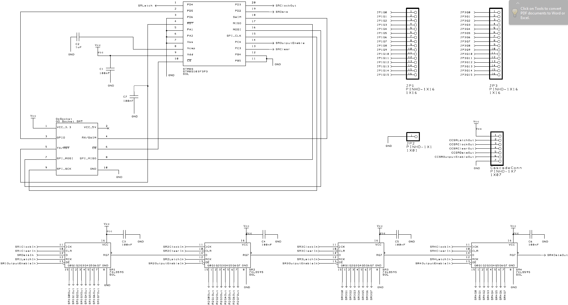
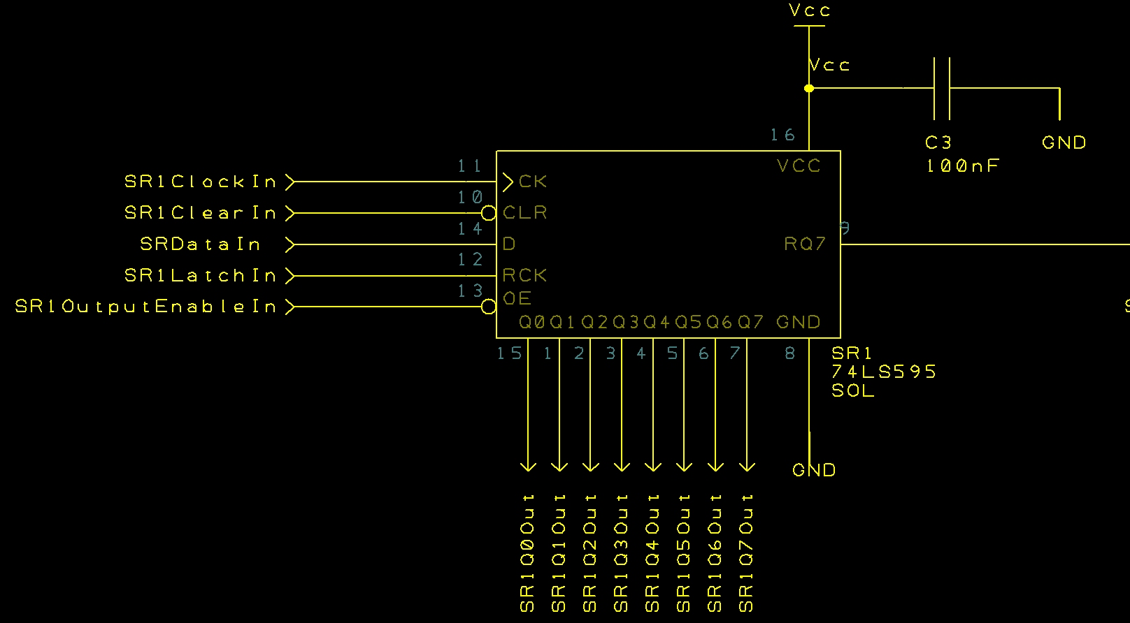
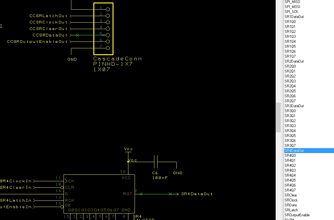
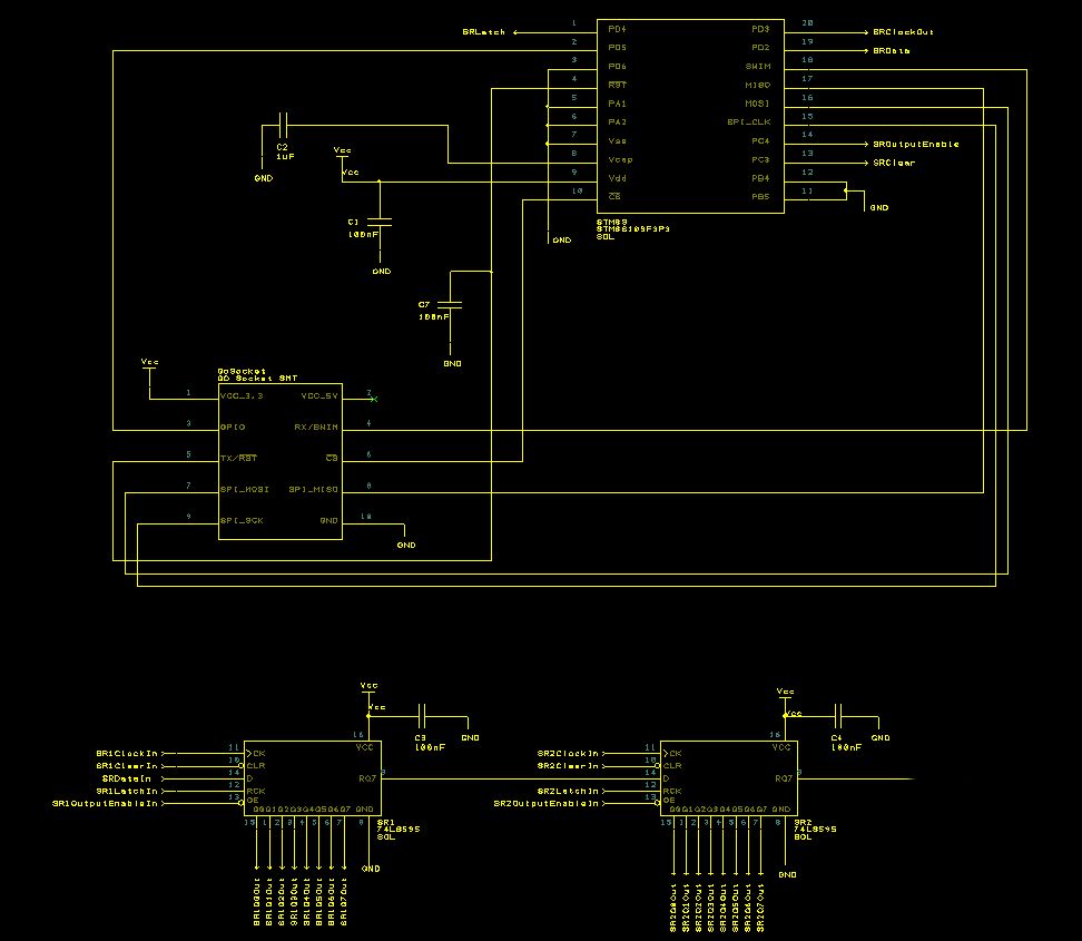
Initialisation should allow for the use of cascaded boards. If you look back at the schematic you will notice a connector called CascadeConn. This connector allows the addition of a simpler board as an expansion module. This board only need to supply additional shift registers leaving the first, main board supplying the logic to communicate with the Netduino GO!. The concept is that if you want 64 outputs then you would have a single Output Expander module with a single, cheaper daughter board.

In order to support the addition of the daughter board the initialisation will need to support the specification of the number of shift registers in the cascade.

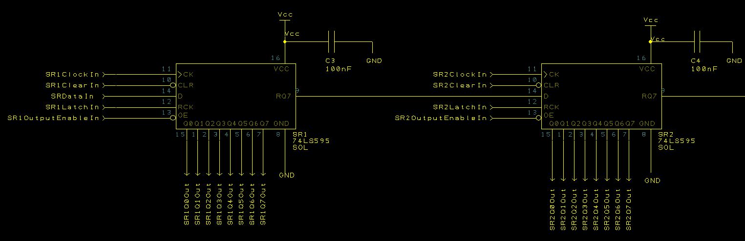
In supporting the cascading of these boards we will also need to provide some sensible default values. The basic case is a single board which contains four shift registers.

We should also consider a maximum value for the number of shift registers. In this case I am going to set this to 12 for two reasons:

  • Power considerations – all of the power for the shift registers is being provided by the Netduino GO!
  • Data packet size – the data packets used in the GoBus are fixed size. Keeping the number of shift registers to a value where only one data packet is required simplifies the communication between the Netduino GO! and the module as a single packet can be used for all messages.

In order to facilitate this we will need code on both the Netduino GO! and the module.

Module Code

The code on the module should allow for the number of shift registers to be set up (assuming a default value of four registers) and then clear the registers. The default code should be called when the module is re-initialised.

//--------------------------------------------------------------------------------
//
//  GO! function 3 - Set up the module.
//
void SetUp()
{
    U8 n = _rxBuffer[2];
    if ((n < 0) && (n < MAX_REGISTERS))
    {
        _numberOfShiftRegisters = n;
        free(_registers);
        _registers = (U8 *) malloc(n);
        ClearRegisters();
        OutputData();
        NotifyGOBoard();
    }
}

Netduino GO! Code

The initialisation code on the Netduino GO! will assume that the startup code on the module will initialise itself to four shift registers. This will reduce the communications overhead between the Netduino GO! and the module. The following when added to the Initialise method should set up the module driver on the Netduino GO! for a variable number of shift registers in the sequence:

//
//  Next, set up the space to store the data.
//
_shiftRegisterData = new byte[numberOfShiftRegisters];
for (int index = 0; index < numberOfShiftRegisters; index++)
{
    _shiftRegisterData[index] = 0;
}
LatchMode = LatchingMode.Automatic;
if (numberOfShiftRegisters != 4)
{
    _writeFrameBuffer[0] = GO_BUS10_COMMAND_RESPONSE;
    _writeFrameBuffer[1] = CMD_SETUP;
    _writeFrameBuffer[2] = (byte) (numberOfShiftRegisters & 0xff);
    WriteDataToModule("Initialise: cannot setup the OutputExpander module");
}

Set Outputs

Setting the outputs is simply a case of sending a number of bytes, one for each shift register to the module.

/// <summary>
/// Set the shift registers using the values in the byte array.
/// "/summary>
/// "param name="registers">Bytes containing the shift register values.</param>
public void Set(byte[] registers)
{
    if (registers.Length != _shiftRegisterData.Length)
    {
        throw new ArgumentException("registers: length mismatch");
    }
    for (int index = 0; index < registers.Length; index++)
    {
        _shiftRegisterData[index] = registers[index];
    }
    Latch();
}

The module code needs a slight adjustment to transfer the correct number of incoming bytes to the register store:

//--------------------------------------------------------------------------------
//
//  GO! function 2 - Output the specified bytes to the shift registers.
//  Tx buffer.
//
void SetShiftRegisters()
{
    for (int index = 0; index < _numberOfShiftRegisters; index++)
    {
        _registers[index] = _rxBuffer[2 + index];
    }
    OutputData();
    NotifyGOBoard();
}

Array of Bits

From a software point of view, a shift register is nothing more than an array of boolean values. Internally it makes sense for the driver to allow this abstraction and use the indexing operator to set a single bit at a time. The code for this operator looks something like this:

/// <summary>
/// Overload the index operator to allow the user to get/set a particular 
/// bit in the shift register.
/// </summary>
/// <param name="bit">Bit number to get/set.</param>
/// <returns>Value in the specified bit.</returns>
public bool this[int bit]
{
    get
    {
        if ((bit >= 0) && (bit < (_shiftRegisterData.Length * 8)))
        {
            int register = bit >> 3;
            byte mask = (byte) (bit & 0x07);
            return ((_shiftRegisterData[register] & mask) == 1);
        }
        throw new IndexOutOfRangeException("OutputExpander: Bit index out of range.");
    }
    set
    {
        if ((bit >= 0) && (bit < (_shiftRegisterData.Length * 8)))
        {
            int register = bit >> 3;
            byte mask = (byte) ((1 << (bit & 0x07)) & 0xff);
            if (value)
            {
                _shiftRegisterData[register] |= mask;
            }
            else
            {
                mask = (byte) ~mask;
                _shiftRegisterData[register] &= mask;
            }
            if (LatchMode == LatchingMode.Automatic)
            {
                Latch();
            }
        }
        else
        {
            throw new IndexOutOfRangeException("OutputExpander: Bit index out of range.");
        }
    }
}

Adding the above code allows the programmer to use constructs such as:

OutputExpander outputs = new OutputExpander();
outputs[2] = true;

instead of the more obscure:

OutputExpander outputs = new OutputExpander();
byte[] data = new byte[4];
data[0] = 0x04;
SetOutputs(data);

Not only is the former example more elegant but it is also more concise.

Clear All Registers

This method will simply clear the shift registers and set the outputs to 0;

/// <summary>
/// This method calls the ClearRegister method on the GO! module and then waits for the
/// module to indicate that it has received and executed the command.
/// </summary>
public void Clear()
{
    _writeFrameBuffer[0] = GO_BUS10_COMMAND_RESPONSE;
    _writeFrameBuffer[1] = CMD_CLEAR_REGISTERS;
    for (int index = 0; index < _shiftRegisterData.Length; index++)
    {
        _shiftRegisterData[index] = 0;
    }
    WriteDataToModule("Clear cannot communicate with the Output Expander module");
}

This method could have been rewritten to set the values to 0 and then send the values to the module. However, the prototype already had an implementation of a clear command and so this was left in as is.

Latch Mode

The introduction of the array indexing operators does introduce on complication, namely that we cannot set all of the outputs to a specified value at the same time without delaying the latching of the registers. Consider the following case:

OutputExpander outputs = new OutputExpander();
outputs[2] = true;
outputs[3] = true;

In this case we would set bit 2 of the lower shift register followed by bit 3 of the same shift register. Because of the speed of .NETMF there would be a slight delay between the two outputs of the shift register being set high. In order to allow for this we introduce the ability to delay the latching of the data from the internal shift register into the output register.

/// <summary>
/// Determine when the data should be sent to the module.
/// </summary>
public enum LatchingMode
{
    /// <summary>
    /// Automtically send the data to the module as soon as there are any changes.
    /// </summary>
    Automatic,
    /// <summary>
    /// Manually latch the data.
    /// </summary>
    Manual
}

/// <summary>
/// Backing variable for the LatchMode property.
/// </summary>
private LatchingMode _latchMode;

/// <summary>
/// Determine how the data will be send to the module.  The default is to 
/// automatically send data as soon as there are any changes.
/// </summary>
public LatchingMode LatchMode
{
    get { return (_latchMode); }
    set { _latchMode = value; }
}

The initialisation of the class would also need to be modified in order to set the mode to automatic:

LatchMode = LatchingMode.Automatic;

The most lightweight method of using the LatchMode is to simply not send the data to the shift registers until the mode is either reset or until the controlling program explicitly latches the data. The Set method will therefore need some adjustment to take into account the two modes:

/// <summary>
/// Set the shift registers using the values in the byte array.
/// </summary>
/// <param name="registers">Bytes containing the shift register values.</param>
public void Set(byte[] registers)
{
    if (registers.Length != _shiftRegisterData.Length)
    {
        throw new ArgumentException("registers: length mismatch");
    }
    for (int index = 0; index < registers.Length; index++)
    {
        _shiftRegisterData[index] = registers[index];
    }
    if (LatchMode == LatchingMode.Automatic)
    {
        Latch();
    }
}

Latch Operation

The introduction of the LatchMode means that we also need to allow for the data to be latched into the shift registers.

/// <summary>
/// Call the Set command on the module to set the outputs of the shift registers.
/// </summary>
private void Set()
{
    _writeFrameBuffer[0] = GO_BUS10_COMMAND_RESPONSE;
    _writeFrameBuffer[1] = CMD_SET_REGISTERS;
    for (int index = 0; index < _shiftRegisterData.Length; index++)
    {
        _writeFrameBuffer[2 + index] = _shiftRegisterData[index];
    }
    WriteDataToModule("Latch cannot communicate with the Output Expander module");
}

The above method simply sends the data to the module.

Testing

We can perform some simple testing of the software while the prototype boards are being made by using the breadboard test environment build in the first post. This board only has two shift registers but it should be possible to test the majority of functionality using this board.

In the previous posts we have cycled through the bits one at a time either from 0 to 15 or down from 15 to 0. In this example we will perform some counting and use the LEDs to display the number in binary. Our test code becomes:

output = new OutputExpander(2);
short cycleCount = 0;
byte[] registers = new byte[2];
output.LatchMode = OutputExpander.LatchingMode.Manual;
while (true)
{
    Debug.Print("Cycle: " + ++cycleCount);
    short mask = 1;
    output.Clear();
    for (int index = 0; index <= 15; index++)
    {
        if ((cycleCount & mask) != 0)
        {
            output[index] = true;
        }
        mask <<= 1;
    }
    output.Latch();
    Thread.Sleep(200);
}

Deploying this application should result in the Netduino GO! counting up from 0 and the binary representation of cycleCount being output on the shift registers. The following video shows this in action:

Conclusion

The above minor modifications to the STM8S module code and the Netduino GO! driver has added the following functionality:

  • Default initialisation to set up for one board
  • Set the bytes for the digital outputs
  • Array like access for the bits
  • Configurable latching mode (automatic or manual)
  • Clear the output
  • Turn outputs from the registers on or off

The code has been carefully written so that we should only need to change two parameters when the final PCBs arrive in order to change the drivers from two shift registers to four shift registers.

A quick test has shown that the main functionality appears to be working on the breadboard prototype as demonstrated by the above video. The prototype PCBs have completed manufacture and are currently with the Hong Kong postal service (as of 27th April 2013). Delivery should take another 7-10 days so there is plenty of time to complete the test suite.

Making a Netduino GO! Module – Stage 4 – Lay Out the Board

Saturday, April 20th, 2013

This series of posts will examine the activities required to take the concept of a module for the Netduino GO! through to production. So far in this series we have completed the following tasks:

  • Created a breadboard prototype
  • Linked the prototype on breadboard to the Netduino GO! with proof of concept software
  • Generated a schematic for a prototype PCB

The next stage of the process is to convert the schematic into a PCB.

This part of the process is the one which is totally new for me and so is the one which has the greatest chance of going wrong. This is where we will find out if my research is good.

The Schematic

Looking back at the previous post we note that we have the following schematic:

Schematic

Schematic

PCB Layout

The PCB layout process converts the schematic into a representation of the board which can be edited using the PCB layout tools. The layout can appear confusing as it is a layered version of the final board. Different colours map to the layers / artefacts on the board. It is this layering which can appear confusing at first.

The layout process requires the following tasks to be completed:

  1. Conversion of the schematic into the ratsnest
  2. Reorganising the components in the ratsnest to their “final” position on the board
  3. Routing the tracks between the components
  4. Addition of additional artefacts such as text
  5. Design Rule Checks (DRC) and verification of the layout
  6. Production of the manufacturing files

It is suggested that the above process is completed in order as each step adds new artefacts to the board.

As noted earlier, the schematic and related files are being created using DesignSpark PCB. The processes being discussed are relevant to PCB manufacture in general.

Making the Ratsnest

The first step in the process is to convert the schematic into a PCB layout. Often this process creates a ratsnest of components and connections with no real layout:

The ratsnest in DesignSpark’s PCB editor shows each component in the footprint it will occupy on the final board. The logical connections between the components are also shown as simple lines between the pads which will be used to mount the components. The lack of structure of the output gives the representation it’s name as it looks like a disorganised rats nest.

Placing the Components

The next step is to lay out the components out on the board. DesignSpark PCB converts the Schematic into a disorganised layout. The Output Expander board is a simple board and reorganising the layout should be simple. The layout can be broken down into the following functional units as follows:

  1. Connectors
  2. Shift registers
  3. Microcontroller

The connectors should near to the edge of the board to allow the board to be connected to the Netduino GO! and external circuitry with ease.

The shift registers and microcontroller can be placed anywhere on the board as we are looking at a low speed, simple board. Placement is more critical for more complex boards. For this board it is logical to place the shift registers near the output from the board as they will used to provide the 32 outputs for the board. It is also logical to place the microcontroller near the Netduino GO! connector as it is receiving instructions from the Netduino GO!.

There are also a number of passive components on the board. These provide some signal filtering and power stabilisation. These components should be place as close to the chip they are supporting. For instance, each of the shift registers has a 100nf capacitor between power and ground. This capacitor provides a buffer for power spikes and it should be placed a close to the chip as possible. There are similar capacitors near the STM8S microcontroller.

So the first step is to take the components and break them down into the logical groups. You can then deal with each group in turn.

The following shows the start of the component placement:

Components on PCB

Components on PCB

The major components are shown along with the connections between the components. This appears a little disorganised at the start as the yellow lines showing the connections between the components run in a straight line taking the most direct route.

Routing the Tracks

Routing is the process of placing copper connections between the components. So at this point you should have the components in their final resting place. If you have to move them later then you will disturb the routing. It is not too big a problem as you can always break the connection and then re-establish it with a new copper track.

The next thing to consider is that for this simple board there are two types of tracks, power and signal. In DesignSpark PCB these are also broken down into two subcategories, nominal and minimum. Where possible I have always selected the nominal connection for both power and signal. You should also remember that it is possible it define your own track type.

When connecting components DesignSpark PCB is reasonably intelligent and will take the connection type from the schematic and apply this to the PCB layout. By default this will be the nominal connection for either power or signal.

Like many PCB layout packages, DesignSpark PCB provides an auto-router. In my experience these take a long time to run and does not always provide a complete board (i.e. they fail to completely route the board) and they also need a reasonable amount of computing power to complete. For a small and simple board like this one I have always found that manually routing the board is the preferred option.

Routing also requires a change in the way of thinking about the board. PCB manufacture is a multi-layer process. The simplest for home manufacture is a single layer. This board can use two layers as this is relatively standard for low cost. Two and four layers are becoming common in the low cost prototype market. Larger numbers of layers are also possible but are currently too expensive and complex for the hobbyist. The simplicity of this board only merits a two layer board which also helps to keep the production cost lower.

Time to start routing…

After a while the board started to come together:

Partially Routed

Partially Routed

The above image shows the partially routed board with some additional artefacts to give an indication how the final board will look. Some important points to note:

  1. Red traces are tracks which will appear on the top layer of the board.
  2. Cyan traces are tracks which are on the lower layer of the board.
  3. Thick tracks are used to carry the ground and power signals.
  4. Thin tracks carry signals between components.
  5. Small yellow circles in the tracks are vias (interconnections between the top and bottom layer of the board).
  6. Component outlines are shown in yellow. These represent the physical size of the component when it is mounted on the board. This will also appear on the top layer silkscreen.
  7. The green parts are represent the board outline and the mounting holes for the board.
  8. All of the changes in direction of a track are mitred rather than simple right angles.

You can see that the board still contains some very thin yellow lines from the original ratsnest. These lines represent the connections which have not been routed yet. A quick check of the connections shows that all of these pads are connected to ground. These pads will become connected when the ground plane is added to the board.

The final routing task is to add a ground plane to the top and bottom of the board.

Top Layer With Ground PlaneTopLayerWithGroundPlane

Top Layer With Ground PlaneTopLayerWithGroundPlane

Adding Additional Artefacts

Now the routing is complete we can return to the additional artefacts on the board. The first and possibly the most important is the board outline. The original outline in the image above was used to give an indication of the maximum ideal board size (10cm x 5cm). Most of the Netduino GO! modules released so far have had rounded corners. So the board outline was replaced by a board with rounded corners.

The next check was to look at the silkscreen layers. These already contain the component outlines along with some names. Some useful additional information includes pin names for the connectors along with some information about the board – a name perhaps.

A final note about the mounting holes. These should be placed on a 5mm x 5mm grid in order to achieve GO! certification. The holes should also be 3.1mm – 3.3mm in diameter.

One limitation I found with DesignSpark PCB is the fact that you cannot place a logo/image in the silkscreen layer (or any other layer for that matter). This is a major limitation of the package. It appears that the solution is to create a font containing the image and then add text to the silkscreen using the font which has been created. For a package which is currently at version 5 seems to be a major omission.

DRC and Verification

The final step in the design process before going to manufacture is to verify the board and determine if the board can be manufactured successfully.

Firstly, print out the board. Now double check the connections making sure that all of the pads are connected correctly. A print out is more useful to me as I can take it away from the screen and start to tick off the pads I believe to be connected correctly.

Now for the DRC check. By default DesignSpark PCB has a set of design rules built in. These rules represent manufacturing parameters such as:

  • Track thickness
  • Minimum spacing between tracks
  • Minimum distance of a component from the board edge

The list is much larger but you get the idea.

I found that the values used for some rules was too cautious and would not let me route some tracks correctly. I had to change the default rules using values from the manufacturer I had decided to use. Rerunning the check with the new minimum values for track spacing allowed the board to pass DRC.

Generate Manufacturing Files

PCB manufacturers use Gerber files. The exact specification of the files used is determined by the chosen manufacturer. For this board we will need to generate a Gerber file in RS-274x format for the following layers:

  • Top layer: pcbname.gtl
  • Bottom layer: pcbname.gbl
  • Solder Stop Mask top: pcbname.gts
  • Solder Stop Mask Bottom pcbname.gbs
  • Silk Top: pcbname.gto
  • Silk Bottom: pcbname.gbo
  • NC Drill: pcbname.txt

One thing to note is that there is nothing to represent the board outline. This has been added to the top silkscreen layer as requested by the manufacturer I have chosen.

The Gerber files are simple text files which contain instructions for the CNC machines used in the manufacturing process.

Now we have the Gerber files it is useful to check that they look right. Luckily there is an on-line Gerber viewer. Uploading your files will allow you to check that the image generated matches the design and layout.

3D View

A neat little feature of DesignSpark PCB is the ability to generate a 3D view of the board being made and to rotate the view. A quick check gives the following images for the final board:

Top of Board in 3D

Top of Board in 3D

Note that the GND pin to the top right of the board has four tabs connecting it to the ground plane.

The cube hovering above the board is the 3D model for the STM8S. A better model could be created, more along the lines of the 75HC595 shift registers. A task for another day…

And rotating the board to view the underside we see the following:

Bottom of Board in 3D

Bottom of Board in 3D

PCB Prototype Manufacturer

The past 12 months have seen a number of PCB companies offer a low cost prototype PCB service. These services allow the production of a number of board (typically 10) starting as low as $10 for 10 5cm x 5cm boards. Some services even give you extra boards if you open source the hardware and hence allow them to add the board to their online shop.

Companies offering this type of service include:

The number of PCB options may be limited (i.e. silkscreen colour etc.) but this certainly makes the cost of production viable. For instance, a 5cm x 10 cm board costs less than $30 including shipping to the UK for 10 boards. Our module has been designed to just fit within the 5cm x 10 cm footprint.

Another service for the hobbyist or prototype developer is that offered by Batch PCB. This company collects the production files from customers and creates a single panelised board containing one or more customer designs. This board is manufactured, the individual boards cut and extracted for shipping to the customer. By doing this the company can offer a low cost production service ($2.50 per square inch at the time of writing) for larger boards.

There are a number of other companies offering low cost services for small runs. The companies quoted are ones I have noted over the past few months when I have been looking for low cost alternatives.

Conclusion

There will now follow a slight pause in the development of the hardware while the boards are produced somewhere in China. According to colleagues it typically takes about one week for manufacture and two weeks for shipping.

This does not mean that development needs to stop. On the assumption that the prototype will work correctly we still have the following tasks which can be completed:

  • Order the components for mounting on the board
  • Develop the drivers

In the next post we will look at developing the drivers for the board using the breadboard prototype as our test environment.

Making a Netduino GO! Module – Stage 3 – The Schematic

Friday, April 12th, 2013

In the previous posts a prototype output expander module was put together on breadboard and connected to the Netduino Go!. A small module driver was developed for the Netduino GO! and the STM8S. This video shows the basic module working:

The next stage in the process is to make the final design decisions and produce a prototype PCB.

Design Criteria

The criteria as defined in the first post stated that the hardware should provide at least 16 digital outputs using low cost components. The breadboard prototype produced shows that we can certainly control 16 digital outputs using the common shift register.

One possible extension is to use more shift registers than were used in the breadboard prototype. This will produce a module with more outputs. A quick look at a local suppliers web site shows that these can obtained for a relatively modest cost. Adding a further two shift registers will take the outputs from 16 to 32.

The prototype shows which pin is being activated by a LED. The LED circuit includes a resistor and MOSFET/Transistor to allow the power for the LED to be provided by an external power supply rather than the 74HC595. Doing this allows the use of LEDs which would exceed the maximum power rating of the 74HC595. Although it should be possible to include these components (resistor and MOSFET) in the final design, they will be omitted in order to reduce the production costs.

In summary:

  1. Use the STM8S as it is low cost and powerful enough for this task
  2. 32 digital output (4 shift registers)
  3. Use 0.1" connectors to the board can be used in breadboard prototyping

PCB Design Software

Over the past few years I have spent a fair amount of time looking for the right PCB design software. I have looked at the following:

There are also several other packages available but these seem to be the three main packages offering free version of their software. Being a hobbyist price is a critical factor in the choice of software to use.

Eagle PCB is available as a free personal edition. The software and licence are both restricted in some way. I have also found the interface to be exceedingly difficult to use. As a long time user of Windows applications the interface in Eagle PCB is counter-intuitive.

KiCad is free and looks to be well supported but I found the interface difficult to use.

DesignSpark looks to be well supported and has gone through several revisions, one major revision in the time in which I have been using the software.

Of the three packages I have settled on using DesignSpark for the following reasons:

  • The interface is the most "standard Windows" like of the three packages
  • Free licence with no restrictions
  • Eagle parts can be imported into the library
  • Additional DesignSpark libraries are also available including one for Sparkfun’s components and boards

DesignSpark is not restricted to producing just the PCB design file but can also render a 3D image of the final PCB. This allows you to visualise how the final board will look. The interface allows the board to be rotated and viewed from an infinite number of points of view.

Schematic

DesignSpark is fairly intuitive to use and there are a number of tutorials and how to guides available and so I will not go into too much detail regarding using the package. There is one tip I would like to give and that is use nets.

Using nets allows the design file to be simplified greatly. You can break the design down into a number of logical components. Consider our design, this breaks down into the following three sections:

  1. STM8S and connector for the GoBus
  2. Shift registers
  3. Connectors for the digital outputs
  4. Now before I discovered how the nets feature works I would have dropped the components for the STM8S and connector on the schematic and then wired them together.

    Next I would have dropped the first of the shift registers onto the schematic and started to connect this to the STM8S. I would have then repeated this with the next shift register (connecting it to the first) and so on. The end result would have been a schematic which was difficult to read due to the number of connecting wires.

    This can be simplified by the use of nets and input/output connectors/pins. So lets have a look at how this appears for the first of out logical blocks, the STM8S and the GoBus connector:


    STM8S Showing Pin Labels

    STM8S Showing Pin Labels

    Looking at the above image you should note that the STM8S has two different connections, an un-named wire which goes off to another part of the circuit (i.e. pins PD5, PD6 etc.) and connections which are terminated with a name (i.e. PD3 is connected to something called SRClockOut).

    The connections which go off of the image are standard interconnects between the various components on the board. These interconnects have been restricted to connecting components in our logical function block (STM8S and GoBus connector). This includes any components required to support the STM8S such as capacitors etc.

    The second group of pins which go to named connections go to either an input or output pin. The names represent the function of the signal; so SRClockOut is the Shift Register Clock Output from the STM8S. If we look at the first shift register you will see that it has an input pin SR1ClockIn (Shift Register 1 Clock Input):

    Shift Register Showing Net Names

    Shift Register Showing Net Names

    We have two pins which have two different names but if we were to look at their properties we would find that they have both been connected to the same net, SRClock Shift Register Clock. By doing this the software knows that the two pins are in fact connected.

    This process has been repeated and a number of nets have been created, some have only two pins on them (the data output from the STM8S – SRData – is only connected to the input of shift register 1), others have several (the SRClock net connected the STM8S clock output pin to the clock input of all of the shift registers).

    Using nets simplifies the schematic and makes it easier to read. Using a standard naming convention for the input and output pins means that you should always be clear on which pins should be connected. It does add a new task to the design process. With a number of the pins named rather than connected you will need to verify that the pins are connected correctly.

    For a small schematic like this one the process of checking the connections is relatively simple. The software allows a component (or net) to be selected from a list of all of the components/nets in the circuit. A part/net is then highlighted on the schematic once it has been selected:


    Net Selection

    Net Selection

    The above diagram shows that the net SR4DataOut has been selected; see the blue highlighted name in the list at the right of the image. The green connections on the schematic show which pins are connected to the SR4DataOut net. Checking is then a case of repeating the process for each of the nets and noting which connections are highlighted.

    The final schematic for the module looks like this:

    Schematic

    Schematic

    A PDF version is also available as this may be difficult to read.

    Conclusion

    Now that we have the schematic we can translate this board into a PCB and from there we can get a 3D view of the board. Here is a sneak preview of the board in 3D:

    Output Expander - 3D View

    Output Expander – 3D View

    In the next post we shall have a look at taking the schematic and laying out the PCB.

Making a Netduino GO! Module – Stage 2 – Connect the GO! to the Breadboard

Friday, April 12th, 2013

In the previous post a prototype for the multiple digital outputs was developed and implemented on breadboard. The STM8S code was independent and demonstrated that two chained 74HC595 shift registers could be controlled by bit-banging data through GPIO pins on the STM8S.

In this post we will continue the development of the module by merging the code from the previous post with the STM8S module code from the post STM8S SPI Slave (Part 3) – Making a Go Module. We will develop both the STM8S code and the NETMF driver to implement the following functionality:

  • Clear the shift registers
  • Set the outputs of the two shift registers

These two functions are already in the standalone version of the STM8S code and it should be a relatively simple exercise to merge this functionality with the Netduino Go Bus communication protocol.

STM8S Application

The first task to be completed for the STM8S code is to create a new project and add the code from the post STM8S SPI Slave (Part 3) – Making a Go Module. The two functions should then be removed and the two new ones we are implementing should be added.

Start a New Project

Start a new STM8S project and save the project into a new directory. Now take the source code in main.c from the project STM8S SPI Slave (Part 3) – Making a Go Module and paste over the code in you new project. Ensure that the project is targeting the correct microcontroller and save the project.

Alternatively, copy the project code from STM8S SPI Slave (Part 3) – Making a Go Module into a new directory.

Remove Dummy Functionality

The project code in the STM8S module post contained a couple of dummy functions illustrating the concept of module functionality and communications. This code should be removed and the application stripped down to the basics required for SPI communication with the Netduino Go!.

Add New Functionality

The final task is to add the code which implements the new functionality as defined for the basic module (i.e. clear the shift registers and set the outputs of the shift registers).

The first thing which is required is to add the #define statements to support the bit-banging:

//--------------------------------------------------------------------------------
//
//  Pins which we will be using for output the data to the shift registers.
//
#define SR_CLOCK            PD_ODR_ODR3
#define SR_DATA             PD_ODR_ODR2
#define SR_CLEAR            PC_ODR_ODR3
#define SR_OUTPUT_ENABLE    PC_ODR_ODR4
#define SR_LATCH            PD_ODR_ODR4

The InitialisePorts method will also need to be modified in order to ensure that the ports above are all setup correctly. We need these to be output ports capable of running at up to 10MHz. The code becomes:

//--------------------------------------------------------------------------------
//
//  Initialise the ports.
//
void InitialisePorts()
{
    //
    //  Initialise Port D.
    //
    PD_ODR = 0;             //  All pins are turned off.
    PD_DDR = 0xff;          //  All pins are outputs.
    PD_CR1 = 0xff;          //  Push-Pull outputs.
    PD_CR2 = 0xff;          //  Output speeds up to 10 MHz.
    //
    //  Initialise Port C.
    //
    PC_ODR = 0;             //  Turn port C outputs off.
    PC_DDR = 0x18;          //  PC3 &amp; PC4 initialised for output.
    PC_CR1 = 0x18;          //  PC3 &amp; PC4 Push-Pull outputs
    PC_CR2 = 0x18;          //  PC3 &amp; PC4 can run up to 10MHz.
    //
    //  Initialise the CS port for input and set up the interrupt behaviour.
    //
#if defined(DISCOVERY)
    PB_ODR = 0;             //  Turn the outputs off.
    PB_DDR = 0;             //  All pins are inputs.
    PB_CR1 = 0xff;          //  All inputs have pull-ups enabled.
    PB_CR2 = 0xff;          //  Interrupts enabled on all pins.
    EXTI_CR1_PBIS = 2;      //  Port B interrupt on falling edge (initially).
#else
    PA_ODR = 0;             //  Turn the outputs off.
    PA_DDR = 0;             //  All pins are inputs.
    PA_CR1 = 0xff;          //  All inputs have pull-ups enabled.
    PA_CR2 = 0xff;          //  Interrupts enabled on all pins.
    EXTI_CR1_PAIS = 2;      //  Port A interrupt on falling edge (initially).
#endif
}

The application will also need some storage space for the data in the shift registers:

//--------------------------------------------------------------------------------
//
//  Number of registers in the chain.
//
#define NUMBER_OF_REGISTERS     2
//
//  Data area holding the values in the register.
//
U8 _registers[NUMBER_OF_REGISTERS];             //  Data in the shift registers.

Note that the variable used to store the data in the registers has been converted into a static array instead of a variable sized array using malloc.

The function table needs to be modified to hold the references to the methods which will implement the module functionality:

//
//  Forward function declarations for the function table.
//
void SetShiftRegisters();
void ClearShiftRegisters();
//
//  Table of pointers to functions which implement the specified commands.
//
FunctionTableEntry _functionTable[] = { { 0x01, ClearShiftRegisters }, { 0x02, SetShiftRegisters } };

The next step is to add the methods which will implement the functionality:

//--------------------------------------------------------------------------------
//
//  Clear the shift registers.
//
void ClearRegisters()
{
    for (U8 index = 0; index < NUMBER_OF_REGISTERS; index++)
    {
        _registers[index] = 0;
    }
}

//--------------------------------------------------------------------------------
//
//  GO! Function 1 - Clear the shift registers.
//
void ClearShiftRegisters()
{
    ClearRegisters();
    OutputData();
    NotifyGOBoard();
}

Note that the functionality has been implemented using two methods, the first ClearRegisters is the internal implementation. This is independent of the Netduino Go! communications and allows the functionality to be called in say the initialisation code of the module. The second method, ClearShiftRegisters is the method which is called by the code as determined by the Netduino Go! driver code. This has the additional output and notification methods which actually sets the data in the shift registers and sends a signal back to the Netduino Go! to let the board know that the request has been received and processed. Note that this split is not necessary but is a design decision taken for this particular module.

The code should be ready to compile and deploy to the STM8S.

Netduino Go! Driver

At this point we should have one half of the communications channel ready to test. The second stage is to implement the driver on the Netduino Go!. As our starting point, we will copy the code from the BasicGoModule class in the post STM8S SPI Slave (Part 3) – Making a Go Module into a new class OutputExpander. We will modify this to add create new functionality to clear and set the shift registers.

Command Constants

The first this we need to do is to remove the old command constants and add two new ones:

/// <summary>
/// Command number for the ClearShiftRegister command.
/// </summary>
private const byte CMD_CLEAR_REGISTERS = 1;

/// <summary
/// Command number for the SetRegister command.
/// </summary>
private const byte CMD_SET_REGISTERS = 2;

Modify the Supporting Methods

The existing code in the module can be optimised for this module. To do this rename the WriteDataToModule method to WriteDataToSPIBus. Now add the following code:

/// <summary>
/// Write the data in the _writeFrameBuffer to the module.  Make several
/// attempts to write the data before throwing an exception.
/// </summary>
/// <param name="exceptionMessage">Exception message to the used in the constructor if the write attempt fails.</param>
private void WriteDataToModule(string exceptionMessage)
{
    int retriesLeft = 10;
    bool responseReceived = false;

    WriteDataToSPIBus();
    while (!responseReceived && (retriesLeft > 0))
    {
        //
        //  We have written the data to the module so wait for a maximum 
        //  of 5 milliseconds to see if the module responds with some 
        //  data for us.
        //
        responseReceived = _irqPortInterruptEvent.WaitOne(5, false);
        if ((responseReceived) && (_readFrameBuffer[1] == GO_BUS10_COMMAND_RESPONSE))
        {
            //
            //  Assume good result, it is up to the calling method to determine if
            //  the command has been executed correctly.
            //
            return;
        }
        else
        {
            //
            //  No response within the 5ms so lets make another attempt.
            //
            retriesLeft--;
            if (retriesLeft > 0)
            {
                WriteDataToSPIBus();
            }
        }
    }
    throw new Exception(exceptionMessage);
}

By making this change we are also making the assumption that the signal back from the module (via the interrupt) is always indicating success. This is a decision which is appropriate for this module but may not be appropriate for other applications/modules.

Add New Functionality

Before adding new functionality it is necessary to remove the existing AddFive functionality from the BasicGoModule.

Out OutputExpander module will provide the application with two basic functions:

  • Clear – clear the shift registers setting the output to 0
  • Set – Set the values in the shift registers to those specified by the parameters

This functionality is provided by the following code:

/// <summary>
/// This method calls the ClearRegister method on the GO! module and then waits for the
/// module to indicate that it has received and executed the command.
/// </summary>
public void Clear()
{
    _writeFrameBuffer[0] = GO_BUS10_COMMAND_RESPONSE;
    _writeFrameBuffer[1] = CMD_CLEAR_REGISTERS;
    WriteDataToModule("Clear cannot communicate with the Output Expander module");
}

/// <summary>
/// Set the shift registers using the values in the byte array.
/// </summary>
/// <param name="registers">Bytes containing the shift register values.</param>
public void Set(byte[] registers)
{
    if (registers.Length != 2)
    {
        throw new ArgumentException("registers: length should be 2 bytes");
    }
    _writeFrameBuffer[0] = GO_BUS10_COMMAND_RESPONSE;
    _writeFrameBuffer[1] = CMD_SET_REGISTERS;
    for (int index = 0; index < registers.Length; index++)
    {
        _writeFrameBuffer[2 + index] = registers[index];
    }
    WriteDataToModule("Clear cannot communicate with the Output Expander module");
}

Testing

At this point we should be able to add some code the Main method of the application to test the module. We will perform something similar to the code in the previous post, we will move a single LED but this time we will illuminate the LED starting a position 15 and working down to 0. This should ensure that we have deployed new code to both the module and the Netduino Go! board.

public static void Main()
{
    OutputExpander output = new OutputExpander();
    int cycleCount = 0;
    byte[] registers = new byte[2];
    while (true)
    {
        Debug.Print("Cycle: " + ++cycleCount);
        for (int index = 15; index >= 0; index--)
        {
            output.Clear();
            if (index < 8)
            {
                registers[0] = (byte) (1 << index);
                registers[1] = 0;
            }
            else
            {
                registers[0] = 0;
                registers[1] = (byte) (1 << (index - 8));
            }
            output.Set(registers);
            Thread.Sleep(200);
        }
    }
}

The test breadboard and Netduino Go! were connected through the Komodex GoBus Breakout Module. This allows the Netduino Go! and the ST-Link/2 programmer to be connected to the breadboard:

Output Expander Connected to Netdunio GO!

Output Expander Connected to Netdunio GO!

And here is a video of this working:

You can just see the Netduino Go! in the bottom left corner of the video.

Conclusion

At this point the basic concept has be proven and the application can perform the following:

  1. STM8S code can control one or more LEDs
  2. STM8S can be controlled using SPI
  3. Netduino Go! can pass instructions to the STM8S

One thing that did become apparent during this part of the process was that both the STM8S code and the Netduino code can be improved by improved grouping the functionality. For instance, in order to add the methods to the function table in the STM8S code I had to jump around the source code a little.

The next step in the process is to look at the hardware and start to prepare for prototype PCB manufacture.

Making a Netduino GO! Module – Stage 1 – Breadboard Prototype

Saturday, April 6th, 2013

So the first stage in the development process (now we have the concept) is to develop a working prototype on breadboard. This will show if we can make the hardware and software work as we want to achieve the desired goals.

Connecting up a Single 74595

For the first stage we will connect up a single 74HC595 shift register to a STM8S chip and write some software for the chip. We are not going to consider connecting the STM8S to other chips/controllers at the moment, we are simply going to output some known data to the shift register and see how it responds.

As this is a simple digital output board we can show the output from the system by using some LEDs. This will also allow us to test one of the secondary objectives, namely the ability to control a reasonable amount of current. The standard 74HC595’s will supply/sink up to 25mA per pin. However, the chip is only rated at 150mW. Turning on all of the pins will over drive the chip. So to get around this we will drive the LEDs through a transistor/MOSFET.

Breadboard Prototype

Looking at the data sheet for the 74HC595 we have 5 control signals to connect to the STM8S:

Pin NamePin NumberDescription
SI14Serial data input
SCK11Serial clock signal
/G or /OE13Output enable
RCK12Transfer data from shift register to the latch
/SCLR10Clear the shift registers

The serial input lines of the 74HC595 lend themselves to the using the SPI bus in order to send data to the shift registers. We will not be able to use SPI in this case as we will need to reserve this for communication with the Netduino Go!.

Connecting the 74HC595

The second shift register should be connected to the same signals as the first except the serial data in line. This should be connected to the serial data output line of the first shift register. In this way the data is cascaded from the first register to the second and so on. The resultant schematic looks this this:

Shift Register Schematic

Shift Register Schematic

The next task is to connect the shift registers to the STM8S. As SPI is already reserved for communicating with the Netduino Go! the data will have to be transferred by bit-banging the data. The following connections should be made between the STM8S and the first 74HC595:

Pin Name74HC595 Pin NumberSTM8S PinDescription
SI14Port D, Pin 2Serial data input
SCK11Port D, Pin 3Serial clock signal
/G or /OE13Port C, Pin 4Output enable
RCK12Port D, Pin 4Transfer data from shift register to the latch
/SCLR10Port C, Pin 3Clear the shift registers

The above schematic becomes:

STM8S and Shift Registers Schematic

STM8S and Shift Registers Schematic

Connecting the LEDs

Visual output from the shift registers will be provided by a number of LEDs. In order to reduce the current drawn from the shift registers the LEDs will be driven by a transistor/MOSFET.

Full Circuit

When assembled, the full circuit looks something like this:

Prototype On Breadboard

Prototype On Breadboard

Software

A small application is required to test the circuit. The first stage is to verify that the STM8S can communicate with the shift registers. The application will simply turn on the various LEDs connected to the shift registers in turn.

Firstly, we need some #define statements to make the code more readable.

#define SR_CLOCK            PD_ODR_ODR3
#define SR_DATA             PD_ODR_ODR2
#define SR_CLEAR            PC_ODR_ODR3
#define SR_OUTPUT_ENABLE    PC_ODR_ODR4
#define SR_LATCH            PD_ODR_ODR4

The application will use a small array of bytes to indicate the status of each pin on the shift register. A small helper function will allow the previous contents of the register to be cleared:

//
//  Clear all of the bytes in the registers to 0.
//
void ClearRegisters(U8 *registers, U8 numberOfBytes)
{
    for (U8 index = 0; index < numberOfBytes; index++)
    {
        registers[index] = 0;
    }
}

The final helper function will output the data to the shift registers:

//
//  BitBang the data through the GPIO ports.
//
void OutputData(U8 *data, int numberOfBytes)
{
    //
    //  Initialise the shift register by turning off the outputs, clearing
    //  the registers and setting the clock and data lines into known states.
    //
    SR_OUTPUT_ENABLE = 1;               //  Turn off the outputs.
    SR_LATCH = 0;                       //  Ready for latching the shift register into the storage register.
    SR_DATA = 0;                        //  Set the data line low.
    SR_CLOCK = 0;                       //  Set the clock low.
    SR_CLEAR = 0;                       //  Clear the shift registers.
    __no_operation();
    SR_CLEAR = 1;
    //
    //  Output the data.
    //
    for (int currentByte = 0; currentByte < numberOfBytes; currentByte++)
    {
        U8 b = data[currentByte];
        for (int index = 7; index >= 0 ; index--)
        {
            SR_DATA = ((b >> index) &amp; 0x01);
            SR_CLOCK = 1;               //  Send a clock pulse.
            __no_operation();
            SR_CLOCK = 0;
        }
    }
    //
    //  Set the clock line into a known state and enable the outputs.
    //
    SR_CLOCK = 0;                       //  Set the clock low.
    SR_LATCH = 1;                       //  Transfer the data from the shift register into the storage register.
    SR_OUTPUT_ENABLE = 0;               //  Turn on the outputs.
}

The final code required is the main program loop which will drive the shift registers:

//
//  Main program loop.
//
void main()
{
    //
    //  Initialise the system.
    //
    __disable_interrupt();
    InitialiseSystemClock();
    //
    //  PD3 and PD2 are used for the serial data going to the registers.
    //  Configure Port D for output.
    //
    PD_ODR = 0;             //  All pins are turned off.
    PD_DDR = 0xff;          //  All pins are outputs.
    PD_CR1 = 0xff;          //  Push-Pull outputs.
    PD_CR2 = 0xff;          //  Output speeds up to 10 MHz.
    //
    //  PB4 and PB5 are used for control of the output and clearing the
    //  registers.  Configure Port B for output.
    //
    PC_ODR = 0;             //  All pins are turned off.
    PC_DDR = 0xff;          //  All pins are outputs.
    PC_CR1 = 0xff;          //  Push-Pull outputs.
    PC_CR2 = 0xff;          //  Output speeds up to 10 MHz.
    __enable_interrupt();
    //
    //  Main loop really starts here.
    //
    numberOfRegisters = 2;
    registers = (U8 *) malloc(numberOfRegisters);
    ClearRegisters(registers, numberOfRegisters);
    OutputData(registers, numberOfRegisters);
    while (1)
    {
        int counter = 0;
        while (counter < 16)
        {
            ClearRegisters(registers, numberOfRegisters);
            if (counter < 8)
            {
                registers[0] = (1 << counter);
            }
            else
            {
                registers[1] = (1 << (counter - 8));
            }
            counter++;
            OutputData(registers, numberOfRegisters);
            for (long index = 0; index < 100000; index++);
        }
    }
}

The code above turns on an LED, pauses and then moves on to the next LED. This is repeated until all of the LEDs have been illuminated. The cycle then repeats from the start. The following video shows this working:

Conclusion

At this point we have proven that the STM8S can be connected to the shift registers and we can turn on one of more LEDs connected to the output of the shift registers.

The next post in this series will connect the STM8S to the Netduino Go! and present a basic driver for the Netduino Go!, enough to illustrate that the Netduino Go! can control the shift registers.

Making a Netduino GO! Module

Saturday, April 6th, 2013

This series of posts will examine the activities required to take the concept of a module for the Netduino GO! through to production.

Project Definition

A simple project will allow the series of posts to concentrate on the principles required for the production of a Netduino GO! module without being too distracted by the functional aspects of the module. The following project definition should meet this brief:

  • Provide 16 or more digital outputs
  • Work with the Netduino GO!
  • Low cost manufacture
  • Use simple tried and tested components/techniques

Meeting the Objectives

As you can no doubt see, this is a reasonably simple project and with the exception of cost, we should have no major problems reaching the objectives. The most obvious solution to this problem is to look at using 74HC595 serial to parallel chips. These are cheap components and the techniques needed to solve this type of problem are tried and tested. The project definition looks like the counting example which is discussed in the Counting Using 74HC595 Shift Registers post with the addition of the Netduino Go! functionality.

Project Plan

Initial assessment of the project indicates that the following steps are required in order to take the project from concept to manufacture:

  1. Build a hardware prototype using the STM8S103F3 to control two shift registers. This will have some form of visual output to prove that we can control the digital lines (probably some LEDs)
  2. Write the software for the STM8S which will control the output of the 74HC595 chips
  3. Generate the schematic for the board
  4. Layout a prototype board and send to manufacture
  5. Write the software for the Netduino GO! while waiting for the manufactured boards to turn up
  6. Assemble a prototype on one of the prototype boards
  7. Conclusion

The first post in the series will build the breadboard prototype and start to control the LEDs using the STM8S.