Arithmetic Logic Unit
Monday, June 26th, 2017The February post regarding the SSEM presented a software implementation of the core hardware:
- Program counter a.k.a Current Instruction (CI)
- Arithmetic Logic Unit (ALU)
- Instruction register a.k.a Present Instruction (PI)
- Registers (memory)
So, how easy this would be to implement the ALU in 1970s hardware, namely, 74LS series of chips.
Arithmetic Logic Unit
The only explicit arithmetic operation implemented by the ALU is the SUB instruction. There is however, one other operation that requires an arithmetic operation to be performed, the JRP instruction. This instruction adds the contents of a store line to CI and stores the result in CI. The inclusion of an ADD instruction to the ALU instruction set will support the JRP instruction.
Before we progress further it is worth noting that the SSEM uses twos complement representation to store numbers.
The high level view of the ALU and the way in which it interacts with the other components can be viewed as follows:
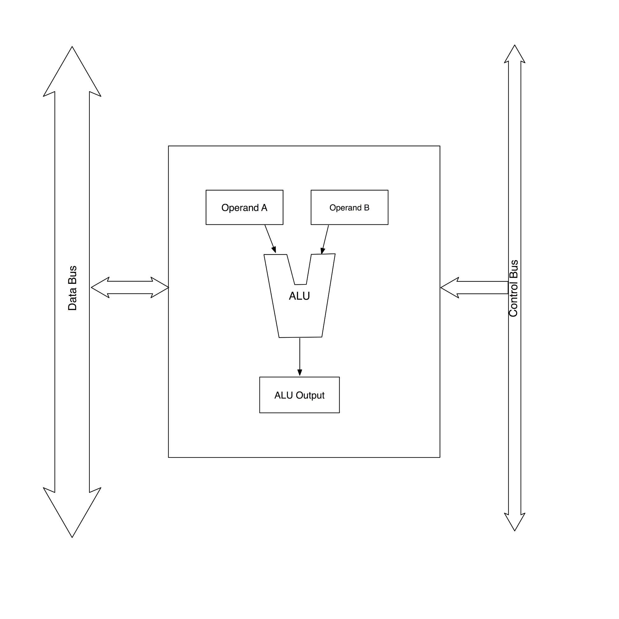
High level view of an Arithmetic Logic Unit.
Two busses run through this CPU:
- Data Bus
- Control Bus
The Data Bus is used to move data from one part of the CPU to another. This is also connected to the external data bus of the computer allowing the CPU to store and retrieve data from system peripherals and memory.
The Control Bus determines which operations are performed by the CPU (in this particular case, by the ALU) at any point in time.
The ALU uses two input operands (A and B) from the Data Bus. Operations are performed on the two operands, the type of operation is determined by the signals on the Control Bus. The results of the operation are then placed in the ALU Output register. The final step is to make this result available to the Data Bus.
The fact that the SSEM implements only these two arithmetic instructions operating on twos complement numbers leads to a very simple ALU design with very few control signals.
Data Bus
As noted, the data bus moves data around the system. The ALU requires two operands for the ADD or SUB operations. These can be implemented in a single operation or in several stages.
Single Operation
Supplying the data in a single operation would require the data bus to be twice as wide as the word size. In the case of the SSEM this would require a data bus that is 64-bits wide. Operand A would be supplied by one half of the signals on the data bus. Operand B would be supplied by the signals on the other half of the bus.
Multiple Steps
Supplying each operand independently would require a two step process, the first step puts operand A on the data bus and loads into the operand A register. The second step puts operand B on the data bus and loads the data into the operand B register. This is slower, taking two steps, but simplifies the hardware design as a 32-bit data bus is used.
Control Bus
The operation of the CPU is orchestrated by the signals present on the control bus. In the case of the instructions being implemented (ADD and SUB) using two registers the following signals are required:
- Load operand A (place the contents on the data bus into operand A)
- Load operand B (place the contents on the data bus into operand B)
- Output result (place the ALU result onto the data bus)
- Add or subtract (Select either addition or subtraction)
There is another instruction that would benefit from having access to the ALU, namely, Load Negative (LDN). This instruction loads a negative number into the accumulator. A negated number can be obtained by subtracting the original number (from a store line) from 0.
If we design the system so that the subtrahend (the number to be subtracted) is always placed in the B operand and operand A can be zero then we can support the LDN instruction. This leads to the final signal, Operand A or Zero.
The full list becomes:
- Load operand A (place the contents on the data bus into operand A)
- Load operand B (place the contents on the data bus into operand B)
- Output result (place the ALU result onto the data bus)
- Add or subtract (Select either addition or subtraction)
- Operand A or Zero
Inside the ALU
If we add the data paths and control signals to the above diagram we have the following:
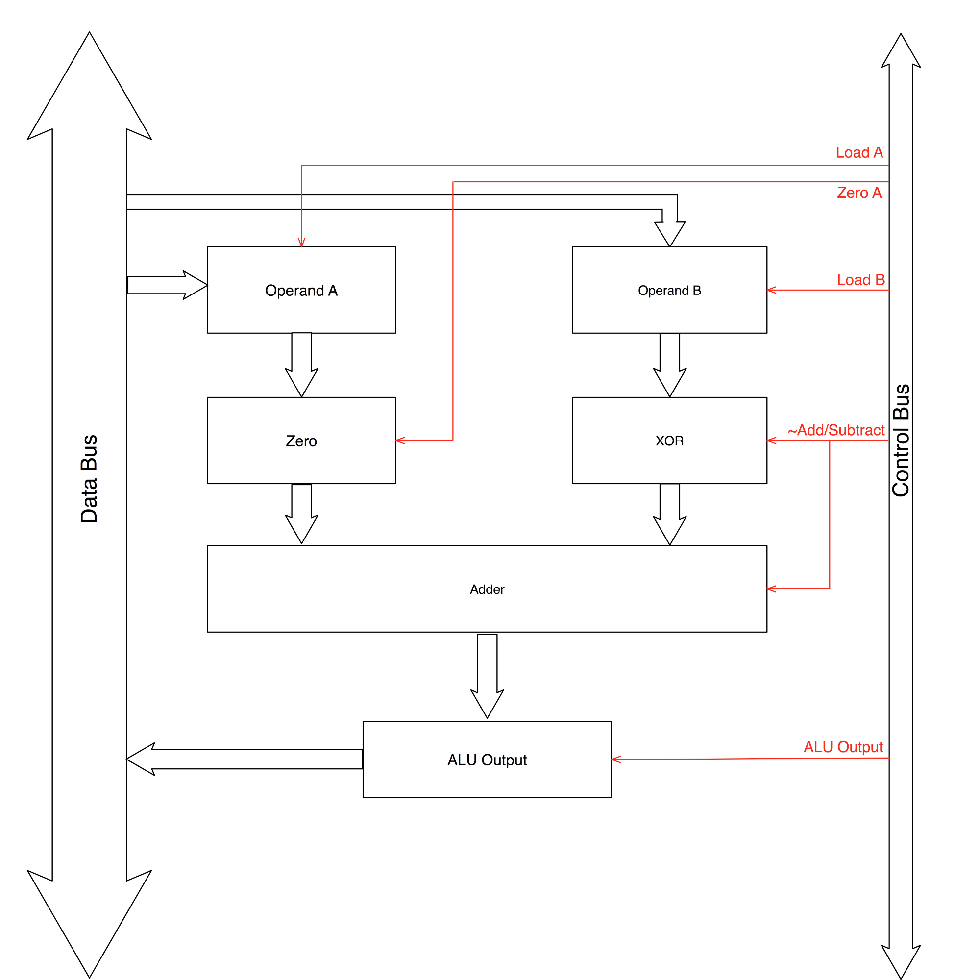
Internal view of an Arithmetic Logic Unit showing the control signals and data paths.
The data paths are shown as broad arrows. The control signals are drawn in red.
Loading the Operand Registers
The data from the data bus is presented to both the A and the B operands at the same time. The data is loaded into the register when the appropriate Load A or Load B signal is set.
Zero Operation
The zero operation is only needed for the A operand. This block will either pass the value in operand A through to the adder (for the SUB, ADD and JRP instruction) or pass 0 through to the adder (for the LDN instruction).
XOR
The XOR block is used to help with the negation of the number in the B operand. In twos complement, a negative number is obtained by inverting the bits in the original number and the adding 1. The XOR helps with the inversion process. Consider the truth table for the XOR operator:
| Control Signal | Input Value | Output |
| 0 | 0 | 0 |
| 0 | 1 | 1 |
| 1 | 0 | 1 |
| 1 | 1 | 0 |
Note that when the Control Signal is 0 then the output from the XOR gate reflects the value on the Input Value. When the Control Signal is 1 then the output is the inverse of the Input Value.
This provides a method for solving the first part of the problem of generating the twos complement negative number, namely, inverting all of the bits in the positive number.
Adder
The adder does exactly what it’s name suggests, it adds two numbers together. Normally, these units have a carry in and a carry out signal to allow multiple units to be chained together:

Two chained four bit adders.
When the ~Add/Subtract control signal is set to 0 then the XOR block passes through operand B unchanged. The carry in signal to the first of the adders (Adder-0) is set to 0. The result is that operand A and operand B are added together. This supports the JRP instruction which requires an addition.
When the ~Add/Subtract control signal is set to 1 then the XOR block inverts the bits in operand B. The additional 1 needed for the twos complement process is provided by passing the ~Add/Subtract control signal to the carry in input to the first adder unit (Adder-0 in the above diagram).
Result Output
The final part of the problem is to control when the result from the calculation is output on to the data bus.
Conclusion
A lot of theory, next step is to consider how this can be put into practice.
Something for the next article.

