RSS

Posts Tagged ‘LED’

TLC5940 16 Channel PWM Driver

Saturday, October 8th, 2011

I have recently been working with the TLC5940 LED Driver chip. This provides 16 PWM outputs which can be used to drive common anode LEDs and I suspect motors etc. For the moment I will be using it to drive 16 LEDs to prove the principle and work out how to interface the chip to the Netduino Mini.

The article and code contained here should allow the creation of a circuit capable of doing the following (and a whole lot more):

Objective

The objective of this exercise is to use the TLC5940 to control 16 LEDs under the control of the Netduino Mini. This will require the following to be developed:

  • Timer circuit to control the grey scale output.
  • Control signals and reference voltage to control the output of the TLC5940
  • Control logic and software for the Netduino Mini

A description of PWM and how it works is assumed. If you require more information then you can check out the Wikipedia article on PWM.

Timer (Clock) Circuit

The TLC5940 uses an external timing signal to control the 16 grey scale outputs to the LEDs. This signal can be as high as 30 MHz. The design presented here uses an 8 MHz crystal / resonator. When I was developing the circuit I have little knowledge of how to build the timer and so used a NE555 configured as a 40 kHz astable oscillator. This was crude but was good enough to start the project. The final design uses an oscillator circuit from a document recommended by Mario on the Netduino forums. You can read the original post here. Mario recommended circuit 1d which is the one I finally used:

8 MHz Timer Circuit.

The final inverter is not really necessary but the chip contains 6 inverters and I was only using two so I fed the output from the timer through an final inverter. This had the effect or producing a squarer signal – although the final signal is still slightly rounded.

In the final circuit I actually used a resonator. I simply dropped this in place of the crystal connecting the outer two pins to the logic gates and the centre pin to ground.

Control Signals

As well as the clock signal, the TLC5940 requires several control signals to determine how the chip should treat the grey scale data. This section looks at each signal and describes its function.

BLANK (Pin 23)

This pin determines the output state of the TLC5940. When this pin is high the outputs are turned off. Setting the pin low turns the outputs back on. More importantly, it changes the internal counter for the PWM control and resets the counter to 0. It is to this counter to which we now turn out attention.

The TLC5940 uses 12 bits to determine the output level for the LEDs connected. Each LED is controlled independently and the full array of 12 bits requires a total of 192 bits (12 bits x 16 LEDs) of data to determine the output levels for the LEDs. The 12 bits for each LED gives a total of 4096 (remember this number, we’ll be using it later) levels for each LED (0 to 4095 inclusive). The TLC5940 uses this data and the current counter to determine the output state of each OUT pin.

Setting BLANK to high and then low causes the counter to be set to zero. An incoming clock pulse causes the counter to be incremented by 1. The chip then turns on all of the outputs which have a greyscale value which is non-zero. Each subsequent pulse cause the chip to do the following:

  1. Increment the counter
  2. For each output compare the counter with the greyscale value for the output pin. If the value is greater than the counter then turn the output on, else turn the output off.

This process repeats until the internal counter reaches 4095 at which point the process stops and the outputs are effectively turned off (the counter value is greater than or equal the output value for the LEDs). This point is important as providing only one pulse to BLANK and a series of 4096 (or more) clock pulses makes this a one time only output. The LED on each output lights for the specified duty cycle and then turns off.

The trick here is to ensure that a BLANK pulse is generated for every 4096 greyscale clock pulses. This is achieved by attaching the output from the timer circuit to both the greyscale clock on the TLC5940 and a divider circuit. The divider counts 4096 clock pulses and then outputs a new BLANK signal to the TLC5940 effectively restarting the counting process. So the modified clock circuit looks something like this:

8 MHz Timer with Divider

The clock signal is split and one connection to the GSCLK (grey scale clock) pin on the TLC5940, the other connection is to the clock inputs of a 14-bit counter/divider (74HC4060). The divider counts the clock pulses and sets the output pins of the chip to represent the current value of the counter. The counter is reset once it reaches the maximum value and the whole process restarts. The counter does not output the lower three bits but this is not an issue for us as we are interested in counting to 4096. We can use the output from bit 12 (2 ^ 12 = 4096) as a BLANK signal for the TLC5940. So for the first 4095 pulses the TLC is setting the outputs according to the values held for each pin. When the counter reaches 4096, the TLC stops displaying data but then a BLANK pulse is received from the divider. This then restarts the whole process. The result, we have the outputs continuously cycling the the LEDs on for the required duty cycle.

One final point about the BLANK signal. This could be used by the microcontroller which is controlling the circuit to turn off the outputs. To allow for this, the output from the divider is ORed with the BLANK signal coming from the microcontroller. The output from the OR gate is passed on to the TLC5940.

VPRG (pin 27)

This signal determines the type of data being transmitted to the TLC5940.

When VPRG is high the chip expected 96 bits of data for the Dot Correction (DC) registers. The DC registers allow the controller to scale the output current supplied at each output pin. This is covered later in this article.

When VPRG is low, the TLC5940 expects 192 bits of data for the grey scale registers.

XLAT (pin 24)

A low-high pulse on this pin latches the data received from the microcontroller into the DC or the GS registers. The data is latched on the rising edge (i.e. low to high) of the XLAT signal.

DCPRG (pin 19)

This pin is not used in this circuit and to connected to Vcc

IREF (pin 20)

This pin can be used to set the maximum current output on each of the output pins. This is done by connecting the pin to ground through a resistor. The value of the resistor is determined by the following calculation:

R = (1.24 / Imax) * 31.5

Where Imax is the maximum current to be supplied. The value of 1.24 is the reference voltage on the IREF pin.

For the LEDs I am using I want a maximum current of about 26mA. This gives a resistor value of 1502 ohms, so a 1k5 resistor should do here.

XERR (pin 16)

This pin is an output from the TLC5940 and can be used to report when an error is detected. This pin is not used in this project and is connected through a 10K pull-up resistor to Vcc.

Grey Scale and Dot Correction

The TLC5940 uses a value in the range 0-4095 to represent the duty cycle for each of the outputs. This gives an effective brightness for each LED given by the following calculation:

Percentage brightness = (Grey Scale value for output N / 4095) * 100

The dot correction reduces the current flowing through the output pins. This can have two effects, it can be used to adjust the current to bring it in range for a specific LED or it can be used to fine tune the output current for an output pin. This can effectively reduce the brightness of a LED. The change in maximum current for a pin is given by the following calculation:

Iout = Imax * (Dot correction value for pin N / 63)

Where Imax is set using the resistor connected to the IREF pin (discussed above).

Final Circuit

The final circuit looks like this:

TLC5940 Full Control Circuit

Controlling the Chip

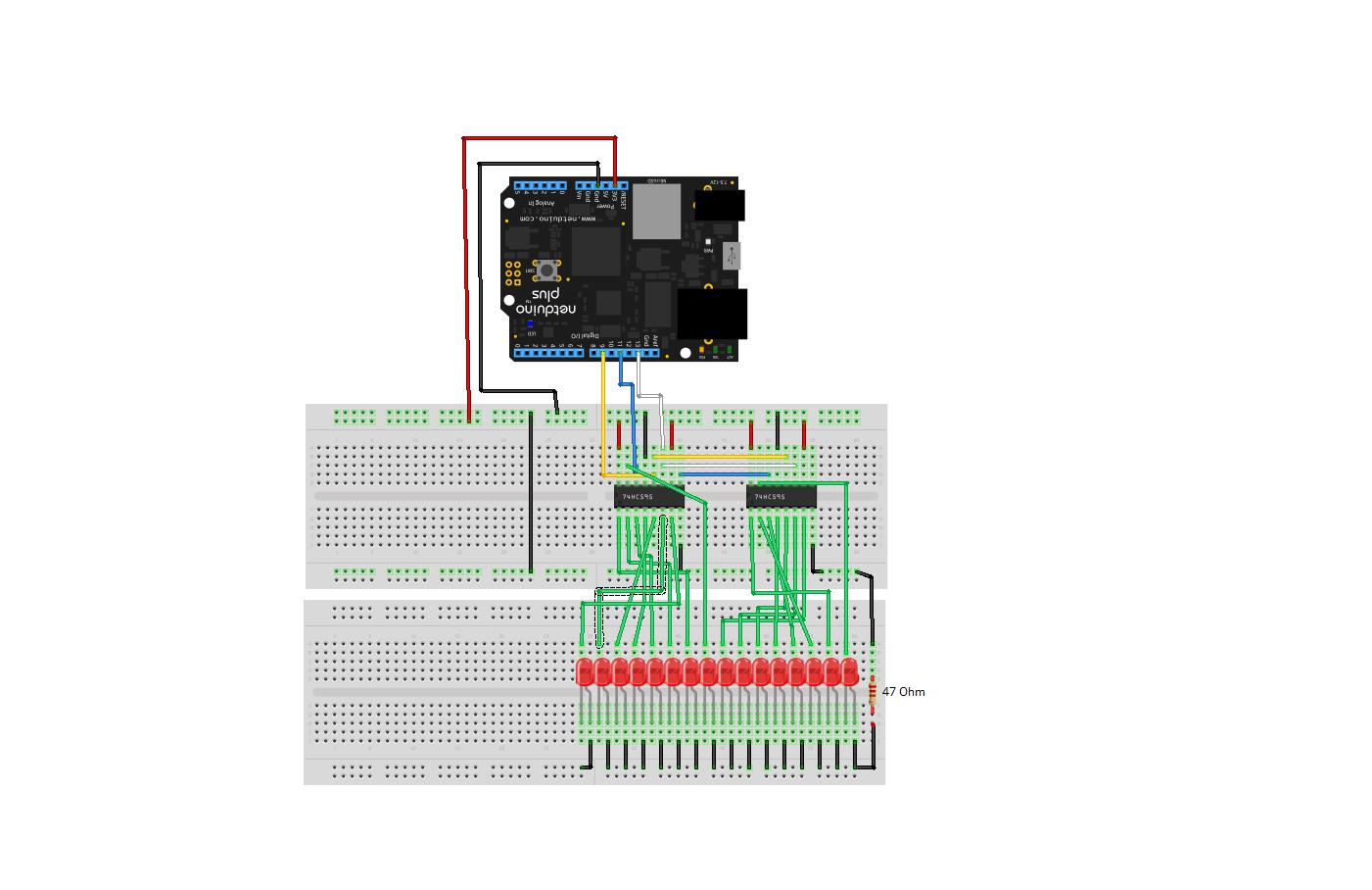
The whole circuit is controlled using a Netduino Mini. The four pink control lines in the above circuit are used by the Netduino Mini to control the TLC5940.

Pin Name Description
MOSI / SIN Serial data output from the Netduino Mini (pin 14 on the Netduino Mini)
SPCK / SCLK Clock signal for the serial data (pin 16 on the Netduino Mini)
XLAT Data latch signal. This could be connected to the chip select although in the initial implementation this is broken out to it’s own pin.
VPRG Determine the programming mode for the TLC5940. High: Dot Correction data is being loaded. Low: Grey Scale data is being loaded.
BLANK Turn the outputs (LEDs) on or off. High: Outputs off. Low: Outputs on.

The application encapsulates the TLC5940 functionality in a single class Tlc5940. This project only deals with one chip controlling 16 outputs (even though several can be linked together). The class only exposes 2 methods:

  • Constructor
  • Display

Constructor

The constructor sets up the system to use the SPI interface and takes parameters to determine which additional control pins should be used.

Display

The display method takes two parameters, one for each of the dot correction data and one for the grey scale data.

The main program contains a small demonstration of the functionality of this class and the TLC5940 chip. It slowly fades in 16 LEDs from off to full brightness and then fades them out to the off state again. This is repeated in a loop forever. For an example of the output see the video at the top of this article.

The code is pretty well commented and so further discussion is not provided here.

You can find the source code here (TLC5940.zip).

Conclusion

This article is really a starter for this chip as there is a whole lot more which is possible. There are a number of areas where I would like to expand both the code and the circuit, namely:

  • Resetting the counter when it reaches 4096. At the moment this runs on until it reaches the maximum value.
  • Use the dot correction values to allow different LEDs to be used on each pin. Different LEDs have different forward currents and this can be fine tuned using the dot correction data to allow the maximum brightness to be achieved by each individual LED.
  • Look at using the CS pin on the SPI interface for the BLANK signal from the Netduino Mini to the TLC5940.
  • Add some error checking code to check if the TLC5940 has detected any errors.
  • Link two or more TLC5940’s together.

Adding these features will make this class more rounded and fully encapsulate the feature set offered by this circuit.

The Cube Goes Travelling

Wednesday, September 21st, 2011

The first cube was completed in July and the initial posting generated some interest. I agreed to make a second and this one has just completed it’s first transatlantic journey and has made an appearance at MakerFare in New York. The following image appeared on Time Out New York’s web site:

LED Cube at Maker Faire September 2011

Building the second cube was fun as I was able to implement all of the lessons learned from making the first cube.

8 x 8 x 8 LED Cube – Powered by Netduino

Sunday, July 10th, 2011

I’m just about to start to write this up but I thought I’d share the cube working before I do. Here is a video showing a few animations:

Watch this space for more information over the coming days.

So What’s All This About a Matrix?

Tuesday, July 5th, 2011

In a previous post I mentioned that replacing a single LED in the centre of a matric would be murder and so it will be. The matrix I have in mind is an 8 x 8 x 8 LED cube controlled by a Netduino board. Now it should be obvious that there are not enough pins to connect 512 LEDs to the Netduino without some magic being involved. This is where the Persistence of Vision post comes into the picture. In theory, it should be possible to control an array using a group of shift registers and a multiplexer circuit. So for the next few weeks this is what I’ll be looking at.

Multi-Threading

The previous post on Persistence of Vision had a simple while loop which allowed 16 LEDs to be controlled from the main program loop. In the final program this will be too cumbersome and timing is almost certainly to become an issue. To overcome this we will need to have the display logic separated from the control logic. This will allow the display to be continuously updated whilst the main program loop is working out what should be displayed next. The following tests this concept by turning on on LED at a time in a bank of 8. If this project has a chance of working then the 8 LEDs should all appear to be switched on permanently.

Hardware

The hardware is relatively simple. We have one shift register connected to the Netduino. This is in turn connected to 8 LEDs through current limiting resistors. The schematic looks something like this:

Persistence of Vision Threaded Display Driver Test Circuit

Software

The software requires us to take the display logic from previous posts and add this to a new class. This class will need to have a method executing in it’s own thread in order to allow the main program and the display driver to run at the same time. So splitting the display code into it’s own class we get something like this:

class LEDCube
{
    /// <summary>
    /// SPI bus to use to send data to the shift registers.
    /// </summary>
    SPI spi = null;

    /// <summary>
    /// CSPI bus configuration
    /// </summary>
    SPI.Configuration config;

    /// <summary>
    /// Buffer holding the display data.
    /// </summary>
    private byte[] buffer;

    /// <summary>
    /// Constructor for the LEDCube class.
    /// </summary>
    public LEDCube()
    {
        config = new SPI.Configuration(SPI_mod: SPI.SPI_module.SPI1,
                                       ChipSelect_Port: Pins.GPIO_PIN_D9,
                                       ChipSelect_ActiveState: false,
                                       ChipSelect_SetupTime: 0,
                                       ChipSelect_HoldTime: 0,
                                       Clock_IdleState: true,
                                       Clock_Edge: true,
                                       Clock_RateKHz: 400);

        spi = new SPI(config);
        buffer = new byte[1];
        buffer[0] = 0;
    }

    /// <summary>
    /// Main loop which continuously updates the display from the buffer.
    /// </summary>
    public void DisplayBuffer()
    {
        while (true)
        {
            lock (buffer)
            {
                spi.Write(buffer);
            }
        }
    }

    /// <summary>
    /// Change the byte in the display buffer.
    /// </summary>
    /// <param name="b">Byte to put into the buffer.</param>
    public void UpdateBuffer(byte b)
    {
        lock (buffer)
        {
            buffer[0] = b;
        }
    }
}

Much of the code should be familiar, we have the SPI bus and config variables along with a constructor to make a new instance of the SPI bus. The new code is really the DisplayBuffer and the UpdateBuffer methods.

  • DisplayBuffer is the method which has replaced the part of the main program loop which outputs the data to the SPI bus. This method is run in it’s own thread.
  • UpdateBuffer simply copies new data from the caller into the display buffer.

Note that both of these methods use locking to ensure that the methods are thread safe.

The main program loop now looks something like this:

LEDCube cube = new LEDCube();
Thread display = new Thread(new ThreadStart(cube.DisplayBuffer));
display.Start();
while (true)
{
    byte value = 1;
    for (int index = 0; index < 8; index++)
    {
        cube.UpdateBuffer(value);
        value <<= 1;
    }
}

A new LEDCube is created and at first this is not running in it’s own thread. The next two lines create and start a new thread. The thread is executing the DisplayBuffer method. We then start the main program lopp which simply sets each bit in a byte and the updates the buffer in the cube using UpdateBuffer.

Next step, build the control logic for 512 LEDs.

What do you do with 600 LEDs?

Tuesday, July 5th, 2011

Delivery, 600 blue LEDs and a bunch of components. So if I’m going to work with these I need to test them first – replacing a single LED in the middle of the matrix is going to be murder so better make sure they are all good to start with.
600 LEDs
Grab a resistor, power supply and a glass of wine. Be back later.

What matrix – All will become clear in the following posts 🙂

Counting Using 74HC595 Shift Registers

Thursday, June 2nd, 2011

Following the post earlier this week regarding the implementation of a ShiftRegister class which allows the Netduino to control a series of 74HC595 shift registers I had a look at what would be needed to make the system count and show the output in binary on a series of LEDs. What you see here is the result. The hardware is the same as the previous post, only the software has changed.

One of the main desires is to allow the programmer to use the natural language features of C# to work with this class. The modifications should therefore support operations such as assignment, logical and etc. The main program loop for a counter should look something like this:

ShiftRegister shiftRegister = new ShiftRegister(16, Pins.GPIO_PIN_D9);
for (ushort index = 0; index < 10000; index++)
{
    shiftRegister = index;
    Debug.Print("Count: " + index + ", " + shiftRegister.ToString());
    shiftRegister.LatchData();
    Thread.Sleep(100);
}

In order to support this we will need to overload the implicit assignment operator for an unsigned short being assigned to a ShiftRegister instance. This results in the following code:

/// <summary>
/// Overload the assignment operator.
/// </summary>
/// <param name="usi">Unsigned short integer to assign to the register.</param>
/// <returns>New ShiftRegister holding the unsigned short value.</returns>
public static implicit operator ShiftRegister(ushort usi)
{
    ShiftRegister result = new ShiftRegister(16);   // ushorts are 16 bits.

    ushort mask = 1;
    for (int index = 0; index < 16; index++)
    {
        result._bits[index] = (usi & mask) > 0;
        mask <<= 1;
    }
    return (result);
}

This generates some problems with the base shift register class from the last post. Most noteably the creation of the SPI instance. The run-time system will generate an error should the programmer try and create two objects wanting to access the SPI bus. Reading the above code you can see that the assignment overload requires a new ShiftRegister instance to be created. A few changes are therefore required in order to allow the system to share the same interface. In order to allow this, the base class moves the SPI object from a shared instance to a static object. This ensures that only one of these can exist at any time. The remaining modifications to the class support this change and add a ToString() method for debugging. The modified code and a sample test project can be found here and the following video shows the application in action.

Further Developments

The base functionality assumed that the class is the only class wanting to use the SPI bus. The number of chips and breakout boards using is large and so it is likely that the programmer will want to communicate with several slave devices using the same bus. This is allowed using the SPI protocol and for the moment this is left as an exercise for the reader.

74HC595 Shift Registers

Monday, May 30th, 2011

The 7400 family of chips have for many years provided a set chips which implement common logic functions. The 74HC595 is a member of this family and provides an eight bit serial-in, parallel-out shift register. This register also provides a pin which can be used to cascade these chips providing a longer sequence of bits if required. In this post we will look at this chip and implement a C# class which can be used to set / reset individual bits in a series of cascaded shift registers. This is very much a software engineers view on how to access a shift register.

74HC595

Those of you who are familiar with the principles and operations of a shift register can skip the next section and move on the the implementation.

Shift Register Overview

A shift register in its simplest form is a series of bits. Data is shifted into the register using serial communication on bit at a time. Each time a bit is pushed into the shift register it moves all those to the right of it one place to the right with the bit at the end being discarded. For example, consider the following four bit register:

b3b2b1b0
1000

Adding a new bit with the value 0 results in the following:

b3b2b1b0Discarded
01000

The 74HC595 has an additional pin which allows the output of the discarded bit. By feeding this discarded bit into another 75HC595 you can build up a chain of cascaded chips to make a larger shift register.

Hardware

A simple LED driver is used to illustrate the hardware and software principles used. The hardware will use two 74HC595’s (although it is possible to use more) to drive a bank of LEDs (one per output for each chip). The bill of materials becomes:

ItemQuantityNotes
74HC5952
LEDs16One for each output pin on the 74HC595’s.
47 Ohm Resistor1
Netduino Plus1
WireLots of itYou really will need lot of it.

The LEDs are really there just to give an instant visual interpretation of the output from the shift registers and to prove the software is working. The way they are wired up and the resistor used to limit the current means that the more LEDs are powered, the dimmer they will be. The wiring looks something like this:

Shift Register Cascade

Shift Register Cascade

Looking at the diagram, the wiring seems confusing. The green wires show the wiring of the LEDs to the outputs of the shift registers. The outputs of the shift register should be wired to the LEDs from right to left in the order QA through QH. This is probably the most confusing part of the diagram due to the number of connections but these all follow the simple principle of wiring the output from the chip to the LED and then through to ground.

If we throw away the green connections then we have a few key connections:

  1. SI on the left most shift register (pin 14) should be connected to MOSI on the Netduino.
  2. SCK on the left most shift register (pin 11) should be connected to SPCK on the Netduino
  3. /G on the left shift register (pin 13) should be connected to the latch pin on the Netduino
  4. RCK on the left shift register (pin 12) should be connected to ground

When cascading the registers the following connections should be made for the registers to the right of the first register:

  1. Serial Out (pin 9) of the left chip to SI (pin 14) of the right chip
  2. SCK of both chips (pin 11) should be connected
  3. /G on both chips (pin 13) should be connected

The data is fed into the shift registers from the left with bit 0 appearing on the far right. The clock and the enable is fed into both chips at the same time. The serial data is fed into the chip on the far left and is cascaded on to the chip to it’s immediate right. Further chips can be added to the right and cascaded in the same manner. In this way, bit 0 will always be at the far right of the shift registers.

Software

The software used the SPI interface on the Netduino to communicate with the shift registers. An important note in the documentation is that the chip has a two stage process for transferring the data from the input to the output. Each bit is transferred into the shift register on the rising edge of the clock pulse. This is then transferred on to the output on the following rising edge. This is fine for all but the last bit as it will need a rising edge in order to be transferred to the output. Standard SPI has the idle clock set to low. As such this could lead to the final bit not being transferred to the output. In order to overcome this the SPI interface was set to the idle clock being high. The final transition from an active clock to an idle clock will then trigger the transfer of the final bit from the input to the output.

From a software engineers point of view a shift register is nothing more than an array of boolean values and this is the approach that was taken. The software holds an array of boolean values (multiples of 8 bits as the shift registers targeted are 8 bit registers). The software holds an array of values which the programmer can then choose to output to the registers.

The variable declarations become:

/// <summary>
/// Array containing the bits to be output to the shift register.
/// </summary>
private bool[] _bits;

/// <summary>
/// Number of chips required to implement this ShiftRegister.
/// </summary>
private int _numberOfChips;

/// <summary>
/// SPI interface used to communicate with the shift registers.
/// </summary>
private SPI _spi;
The variable holding the number of chips is used to help the runtime performance by not having to recalculate the number of chips on each transfer to the hardware.

The constructor for the class instantiates the array holding the number of bits in the shift register and the SPI interface:

public ShiftRegister(int bits, Cpu.Pin latchPin = Cpu.Pin.GPIO_Pin8, SPI.SPI_module spiModule = SPI.SPI_module.SPI1, uint speedKHz = 10)
{
    if ((bits > 0) && ((bits % 8 ) == 0))
    {
        _bits = new bool[bits];
        _numberOfChips = bits / 8;
        for (int index = 0; index < bits; index++)
        {
            _bits[index] = false;
        }

        SPI.Configuration config;

        config = new SPI.Configuration(SPI_mod: spiModule, ChipSelect_Port: latchPin, ChipSelect_ActiveState: false, ChipSelect_SetupTime: 0, ChipSelect_HoldTime: 0,  Clock_IdleState: true, Clock_Edge: false, Clock_RateKHz: speedKHz);

        _spi = new SPI(config);
    }
    else
    {
        throw new ArgumentOutOfRangeException("ShiftRegister: Size must be greater than zero and a multiple of 8 bits");
    }
}

A little bit operator overloading on the indexer allows the programmer to address the individual bit in the shift register:

/// <summary>
/// Overload the index operator to allow the user to get/set a particular 
/// bit in the shift register.
/// </summary>
/// <param name="bit">Bit number to get/set.</param>
/// <returns>Value in the specified bit.</returns>
public bool this[int bit]
{
    get
    {
        if ((bit >= 0) && (bit < _bits.Length))
        {
            return (_bits[bit]);
        }
        throw new IndexOutOfRangeException("ShiftRegister: Bit index out of range.");
    }
    set
    {
        if ((bit >= 0) && (bit < _bits.Length))
        {
            _bits[bit] = value;
        }
        else
        {
            throw new IndexOutOfRangeException("ShiftRegister: Bit index out of range.");
        }
    }
}

The final piece of the jigsaw is to allow the programmer to send the data to the shift register:

/// <summary>
/// Send the data to the SPI interface.
/// </summary>
public void LatchData()
{
    byte[] data = new byte[_numberOfChips];

    for (int chip = 0; chip < _numberOfChips; chip++)
    {
        data[chip] = 0;
        byte bitValue = 1;
        int offset = chip * 8;
        for (int bit = 0; bit < 8; bit++)
        {
            if (_bits[offset + bit])
            {
                data[chip] |= bitValue;
            }
            bitValue <<= 1;
        }
    }
    _spi.Write(data);
}

This method is really the work horse as it converts the bits into an array of bytes which are transferred to the shift registers.

Testing it Out

Testing should be easy, lets walk through all of the bits for a 16 bit register made by having two shift register connected together:

public static void Main()
{
    ShiftRegister shiftRegister = new ShiftRegister(16, Pins.GPIO_PIN_D9);
    while (true)
    {
        for (int index = 0; index < 16; index++)
        {
            shiftRegister[index] = true;
            shiftRegister.LatchData();
            Thread.Sleep(100);
            shiftRegister[index] = false;
        }
    }
}

This example uses two registers (16 bits) and uses pin D9 as the enable pin for the register. The code sets, displays and then resets each bit starting at bit 0 through to bit 15.

The full code for the shift register class can be found here (ShiftRegister.zip).

4 Digit, 7 Segment Display – Part 1 – Ouput a Byte

Tuesday, March 15th, 2011

Update 18 March 2011: This is where this series of posts finishes for the minute as I appear to have fried the MAX7219 (or something else is wrong with the setup) as I can send commands to it but the output does not make any sense. I’ll have to return to this series when I have a new chip 🙁

This series of posts will discuss using the MAX7219 LED driver chip to drive a four digit, seven segment LED display. The series is made up of the following posts:

  1. Part 1 – Output a Byte (This Post)
    Output a series of bytes from the Netduino Plus using the SPI protocol
  2. Part 2 – Output an Unsigned Short
    Similar to the first post but this time we will write a series of short integers using SPI. This will also start to implement the class which will write the data to the MAX7219 chip.
  3. Part 3 – Displaying Numbers
    Using the MAX7219 class to display a number on the display
  4. Part 4 – Displaying Sensor Data
    Hooking up a sensor to the Netduino and displaying the reading from the sensor.

Background Reading

The following posts provide some background information as these are similar projects:

Objective

The objective of these post is to connect the Netduino Plus to the breadboard and get a 5V logic signal representing a series of bytes. In order to do this it is necessary to convert the output from the Netduino Plus from 3.3V to 5V. I propose to experiment and use a 7408 quad 2 input AND gate to convert the 3.3V signal up to 5V. So for this post we will need the following components:

  1. Netduino Plus
  2. 1 x 74HCT08N quad 2 input AND gate
  3. Breadboard with 5V power supplied to the power rails
  4. Wire to connect the components

Theory

Part of this exercise is to see if we can convert a 3.3V signal into a 5V signal. This is necessary as the MAX7219 uses 5V inputs. The quad input AND gate was chosen to do this for no other reason than I had a few spare in the component box. The data sheet for this chip states that the minimum voltage for a high input is 3.15V when the chip is supplied with 4.5V. A quick experiment shows that a 3.3V input signal to this chip does indeed result in a high output.

So by connecting one of the inputs to the AND gate to 5V and the second to the signal source, then the output from the gate should reflect the input but translated from 3.3V to 5V.

One point to note is that the chip will take a little while for the signal on the inputs to be reflected on the output pins. This application will be running at a low frequency (10KHz) and so the chip should be able to keep up.

Software

The software is a simple starter program which cycles through the bytes from 0 to 255 and output’s these bytes on the SPI bus. The Saleae logic analyser is used to verify that the data is being output correctly. A small test program should demonstrate that the data is being transmitted on the bus correctly:

using System;
using System.Net;
using System.Net.Sockets;
using System.Threading;
using Microsoft.SPOT;
using Microsoft.SPOT.Hardware;
using SecretLabs.NETMF.Hardware;
using SecretLabs.NETMF.Hardware.NetduinoPlus;

namespace NetduinoPlusTestApplication
{
    public class Program
    {
        public static void Main()
        {
            SPI.Configuration config;
            SPI spi;
            byte[] b;

            config = new SPI.Configuration(Pins.GPIO_PIN_D10, false, 0, 0, false, false, 10, SPI.SPI_module.SPI1);
            spi = new SPI(config);
            b = new byte[1];

            while (true)
            {
                for (byte v = 0; v <= 255; v++)
                {
                    b[0] = v;
                    spi.Write(b);
                    Thread.Sleep(20);
                }
            }
        }
    }
}

Hardware

The following table shows how the Netduino Plus is connected to the 74HCT08N

74HCT08NConnection
2, 5, 10, 13, 14+5V
7Ground
12Netduino Plus digital pin 10 (used for CS)
1Netduino Plus digital pin 11 (MOSI)
4Netduino Plus digital pin 13 (Clock)

The ground on the Netduino Plus should also be connected to the ground on the breadboard.

Results

After completing the wiring the logic analyser was hooked up and the following trace appeared:

Scrolling through the trace show each of the ASCII characters being interpreted correctly.

So the next step it to start to build the class which will talk to the MAX7219.

Flashing LED Using an Astable 555

Sunday, February 20th, 2011

This project will use the 555 timer IC to flash an LED with the eventual aim of using the timer to provide a regular timing pulse.

Objective

Use the 555 timer to flash an LED with a period of 1 second.

Components

The timer being used is a standard NE555N timer. This is a cheap general purpose timer circuit and has been around for many years. In fact I remember using them when I first became interested in electronics at school.

The circuit for setting this chip up in astable mode is as follows:

So along with the chip itself we will need 3 resistors, 2 capacitors and an LED. Thye values of R1, R2 and C1 determine the frequency of the pulses according to the following equation:

A frequency of 1 Hz was chosen to make the pulses clearly visible to the observer. A little reordering of the equation and a sift through some standard components gave the following values for these components:

Component Value
R1 1 KOhm
R2 2 KOhms (two 1 KOhm resistors in series)
C1 470 micro Farad

Putting it all together

Gathering all of the components together along with some breadboard gave a LED flashing at approximately 1 Hz. I say approximately as I’ll need to feed that output through a logic analyser / oscilloscope to verify the exact frequency.

RGB LED and PWM

Saturday, February 12th, 2011

Lots of abbreviations in this post but the aim is simple. Going back to working with LEDs, the idea is to control a RGB LED using the Netduino. The LED I have purchased is a common cathode LED the details of which can be found here.

The LED can be used either as a status display (using each of the three colours for a different status) or the three colours can be mixed to provide mixed colour output. This entry describes how to use the Netduino to provide a mixed colour output using PWM.

Wiring Up The Circuit

The LED is a common cathode LED with three anodes, one for each colour (Red, Green and Blue). This will require three pins on the Netduino in order to control the changing colours. Each of the three pins will require a current limiting resistor in order to ensure that we don’t try to draw too much current from the Netduino and burn out the pins. A quick application of Ohms law to ensure that we do not try and draw more than 8mA gave the following nearest equivalent resistors:

ColourVoltageResistor
Red2V220 ohms
Green3.2V20 ohms (2 x 10 ohms)
Blue3.2V20 ohms (2 x 10 ohms)

The next step is to hook up the LED to the Netduino. This is done using three of the four PWM pins on the board. By using PWM we can vary the power supplied to each of the three pins on the LED. This will allow control of the amount of each colour generated which in turn will determine the colour of the LED. The image below shows the circuit set up on breadboard:

Software

The software uses PWM to control the power supplied to the LED. I found two articles which helped in understanding how this works, the first on Wikipedia and the second by Philip on the Netduino forums. The basic principle is that by varying the amount of time a pin is powered we can change the average power supplied by the pin. The following code show how this can be achieved using three of the Netduino’s PWM pins:

public static void Main()
{
    PWM red;
    PWM green;
    PWM blue;

    red = new PWM(Pins.GPIO_PIN_D6);
    blue = new PWM(Pins.GPIO_PIN_D5);
    green = new PWM(Pins.GPIO_PIN_D9);

    while (true)
    {
        for (uint redDuration = 0; redDuration < 4000; redDuration += 1000)
        {
            red.SetPulse(10000, redDuration);
            for (uint greenDuration = 0; greenDuration < 4000; greenDuration += 1000)
            {
                green.SetPulse(10000, greenDuration);
                for (uint blueDuration = 0; blueDuration < 4000; blueDuration += 1000)
                {
                    blue.SetPulse(10000, blueDuration);
                    Thread.Sleep(200);
                }
            }
        }
    }
}

The program simply cycles through a series of values for each of the selected pins and changes the amount of time each pin is active. The result is a LED which constantly changes colour.