RSS

Posts Tagged ‘LED’

Single Conversion ADC on the STM8S

Monday, September 17th, 2012

In this post we will have a look at the Analog to Digital Converter (ADC) on the STM8S microcontroller. The number of ADCs available will depend upon the STM8S you are using. We will be using ADC1 which should be present on all STM8S microcontrollers.

In order to show how the ADC works we will be using the STM8S as a dimmer switch for an LED. This simple example will demonstrate how we can read an analog value and use a PWM signal to control the brightness of an LED.

In order to do this we will need the following:

We will also be using Timer 1, Channel 4 to generate a PWM signal to control the brightness of the LED (see Generating PWM Signals using the STM8S.

The algorithm we will be using is as follows:

  1. Configure the system
  2. Read the value from the ADC
  3. Set the PWM output based upon the analog reading
  4. Pause for 1/10th second
  5. Repeat from step 2

We will achieve this by using interrupts from the following resources:

  • Timer 3 – Generates the PWM signal which will be used to control the LED
  • Timer 2 – 1/10th second interrupt which triggers the ADC process
  • ADC – Conversion is completed, adjust the PWM output

ADC Features

The ADC has several modes of operations. We will be using the simplest, namely single conversion mode. As the name suggests, this mode performs a conversion on a specific channel. We will also instruct the microcontroller to generate an interrupt once the conversion is complete.

Amongst the other features and modes on the STM8S are the following:

  • Single scan mode – Perform a single conversion on a number of channels.
  • Continuous and Buffered Continuous – Perform continuous conversions. New conversions start as soon as the current conversion has completed.
  • Continuous Scan – Similar to the Single Scan but operating on a number of channels. Conversion restarts from channel 0 when the last channel has been converted.
  • Watchdog – Set upper and lower limits for the conversion. An interrupt can be generated if a conversion is above the upper or below the lower values.
  • External Trigger – An external trigger is used to start a conversion.

The conversion takes 14uS after a stabilisation period. Once the stabilisation is complete, readings are available without any further pauses.

The Registers

So let’s have a look at the registers we will be using in order to control the ADC:

  • ADC_CR2_ALIGN – Data alignment
  • ADC_CSR_CH – Channel selection
  • ADC_DRH/L – Analog conversion result
  • ADC_CR1_ADON – Turn ADC on / off, trigger conversion
  • ADC_CR3_DBUF – Data buffer Availability
  • ADC_CSR_EOCIE- Enable ADC interrupts
  • ADC_CSR_EOC – End of Conversion

ADC_CR1_ADON – ADC On/Off

The ADON flag determines of the ADC is on or off. It also determines if a conversion has been triggered. Setting ADON to 0 turns the ADC off. Setting ADON to 1 the first time turns the ADC on. Setting this value a second (or subsequent time) starts a conversion.

ADC_CSR_CH – Channel Selection

The CH flag determines the channel which should be converted.

ADC_CR2_ALIGN – Data Alignment

The ALIGN flag determines the type of alignment in the result registers. We will be setting this to right align (set to 1) the data in the registers.

ADC_DRH/L – Conversion Result

This pair of registers holds the result of the conversion. The order the registers should be read is dependent upon the alignment of the data in the registers. For right aligned data we need to read the DRL before DRH.

ADC_CSR_EOCIE – Enable ADC Interrupts

Turn the ADC interrupts on / off.

ADC_CSR_EOC – End of Conversion

This bit is set by the hardware when the conversion has completed. It should be reset by the software in the Interrupt Service Routine (ISR).

Unused Registers

The application we are going to be writing is simple and only performs a conversion once every 1/10th second. This is plenty of time to perform a conversion and process the data before the next conversion starts. As such, we do not need to check the overrun register. This register indicates if the data generated in the continuous mode was overwritten before it was used.

Hardware

This post requires some additional hardware to be added to the circuit containing the STM8S:

  • LED which is being controller through a transistor configured as a switch
  • Potentiometer to provide an analog signal for conversion

LED Output

Use the LED Output circuit in the post External Interrupts on the STM8S. Connect the base of the transistor to the output of Timer 1, Channel 3.

Potentiometer

Connect the potentiometer so that one pin is connected to ground and one to 3.3V. The output (the wiper) should be connected to AIN4 on the STM8S. I used a 10K potentiometer for this example.

Software

As we have already noted, we will be driving the application by using interrupts. We will also use a few techniques/methods from previous posts. So let’s look at each of the elements we will be using.

Timer 2 – Start Conversions

Timer 2 is used to generate 10 interrupts per second. Each interrupt will trigger a new conversion. Setting up the timer should look familiar:

void SetupTimer2()
{
    TIM2_PSCR = 0x05;       //  Prescaler = 32.
    TIM2_ARRH = 0xc3;       //  High byte of 50,000.
    TIM2_ARRL = 0x50;       //  Low byte of 50,000.
    TIM2_IER_UIE = 1;       //  Enable the update interrupts.
    TIM2_CR1_CEN = 1;       //  Finally enable the timer.
}

The ISR is a simple method, it has only one main function, namely to start the conversion.

#pragma vector = TIM2_OVR_UIF_vector
__interrupt void TIM2_UPD_OVF_IRQHandler(void)
{
    PD_ODR_ODR5 = !PD_ODR_ODR5;        //  Indicate that the ADC has completed.

    ADC_CR1_ADON = 1;       //  Second write starts the conversion.

    TIM2_SR1_UIF = 0;       //  Reset the interrupt otherwise it will fire again straight away.
}

Note the comment on the ADC register Second write starts the conversion. This method assumes that we have set ADC_CR1_ADON at least once previously. As you will see later, we set this register in the setup method for the ADC.

In addition to the starting of the conversion, we have also added a line of code to toggle PD5. This will show us when the ISR has been triggered and is really only there for debugging.

Timer 1, Channel 4 – PWM Signal

The ADC generates a 10 bit value. We will therefore set up Timer 1 to generate a PWM signal which is 1024 (210) clock signals in width. We can therefore use the value from the conversion to directly drive the PWM duty cycle.

void SetupTimer1()
{
    TIM1_ARRH = 0x03;       //  Reload counter = 1023 (10 bits)
    TIM1_ARRL = 0xff;
    TIM1_PSCRH = 0;         //  Prescalar = 0 (i.e. 1)
    TIM1_PSCRL = 0;
    TIM1_CR1_DIR = 1;       //  Down counter.
    TIM1_CR1_CMS = 0;       //  Edge aligned counter.
    TIM1_RCR = 0;           //  Repetition count.
    TIM1_CCMR4_OC4M = 7;    //  Set up to use PWM mode 2.
    TIM1_CCER2_CC4E = 1;    //  Output is enabled.
    TIM1_CCER2_CC4P = 0;    //  Active is defined as high.
    TIM1_CCR4H = 0x03;      //  Start with the PWM signal off.
    TIM1_CCR4L = 0xff;
    TIM1_BKR_MOE = 1;       //  Enable the main output.
    TIM1_CR1_CEN = 1;
}

Note that the Auto-reload registers is set to 1023 (0x3ff). We also set the capture compare registers to 1023 at the start. This will turn the LED off when the program starts.

System Clock

The program will be generating a PWM signal with a reasonably high clock frequency. In order to do this we will set the clock to use the internal oscillator running at 16MHz.

void InitialiseSystemClock()
{
    CLK_ICKR = 0;                       //  Reset the Internal Clock Register.
    CLK_ICKR_HSIEN = 1;                 //  Enable the HSI.
    CLK_ECKR = 0;                       //  Disable the external clock.
    while (CLK_ICKR_HSIRDY == 0);       //  Wait for the HSI to be ready for use.
    CLK_CKDIVR = 0;                     //  Ensure the clocks are running at full speed.
    CLK_PCKENR1 = 0xff;                 //  Enable all peripheral clocks.
    CLK_PCKENR2 = 0xff;                 //  Ditto.
    CLK_CCOR = 0;                       //  Turn off CCO.
    CLK_HSITRIMR = 0;                   //  Turn off any HSIU trimming.
    CLK_SWIMCCR = 0;                    //  Set SWIM to run at clock / 2.
    CLK_SWR = 0xe1;                     //  Use HSI as the clock source.
    CLK_SWCR = 0;                       //  Reset the clock switch control register.
    CLK_SWCR_SWEN = 1;                  //  Enable switching.
    while (CLK_SWCR_SWBSY != 0);        //  Pause while the clock switch is busy.
}

GPIO – Debug Signals

As with previous examples, we will configure some of the output ports so that we can generate debug signals:

void SetupOutputPorts()
{
    PD_ODR = 0;             //  All pins are turned off.
    //
    //  PD5 indicates when the ADC is triggered.
    //
    PD_DDR_DDR5 = 1;
    PD_CR1_C15 = 1;
    PD_CR2_C25 = 1;
    //
    //  PD4 indicated when the ADC has completed.
    //
    PD_DDR_DDR4 = 1;
    PD_CR1_C14 = 1;
    PD_CR2_C24 = 1;
}

ADC

The setup method for the ADC is relatively simple as many of the settings we will be using are the defaults after a reset. This method is as follows:

void SetupADC()
{
    ADC_CR1_ADON = 1;       //  Turn ADC on, note a second set is required to start the conversion.

#if defined PROTOMODULE
    ADC_CSR_CH = 0x03;      //  Protomodule uses STM8S105 - no AIN4.
#else
    ADC_CSR_CH = 0x04;      //  ADC on AIN4 only.
#endif

    ADC_CR3_DBUF = 0;
    ADC_CR2_ALIGN = 1;      //  Data is right aligned.
    ADC_CSR_EOCIE = 1;      //  Enable the interrupt after conversion completed.
}

After calling this method, the ADC should be powered on and ready to perform a conversion. Note that the ADC will not perform a conversion until ADC_CR1_ADON is set for a second time. This will be performed by the Timer 2 interrupt.

Another point to note is that on the Protomodule board the version of the STM8S does not have the AIN4 channel and so we use AIN3 instead.

The next method we will consider is the ADC ISR. This is where the real work of changing the values for the PWM signal takes place.

#pragma vector = ADC1_EOC_vector
__interrupt void ADC1_EOC_IRQHandler()
{
    unsigned char low, high;
    int reading;

    ADC_CR1_ADON = 0;       //  Disable the ADC.
    TIM1_CR1_CEN = 0;       //  Disable Timer 1.
    ADC_CSR_EOC = 0;        //     Indicate that ADC conversion is complete.

    low = ADC_DRL;            //    Extract the ADC reading.
    high = ADC_DRH;
    //
    //  Calculate the values for the capture compare register and restart Timer 1.
    //
    reading = 1023 - ((high * 256) + low);
    low = reading & 0xff;
    high = (reading >> 8) & 0xff;
    TIM1_CCR3H = high;      //  Reset the PWM counters.
    TIM1_CCR3L = low;
    TIM1_CR1_CEN = 1;       //  Restart Timer 1.

    PD_ODR_ODR4 = !PD_ODR_ODR4;     //  Indicate we have processed an ADC interrupt.
}

Note that we once again use a GPIO port to indicate when the ISR has been called.

Main Program Loop

The main program loop looks pretty much like the programs we have written in previous examples:

void main()
{
    //
    //  Initialise the system.
    //
    __disable_interrupt();
    InitialiseSystemClock();
    SetupTimer1();
    SetupTimer2();
    SetupOutputPorts();
    SetupADC();
    __enable_interrupt();
    while (1)
    {
        __wait_for_interrupt();
    }
}

Results

If we put all of this together we can do the following:

The LED indicates the duty cycle of the PWM signal. The output on the oscilloscope confirms the changes being made to the PWM signal (the wider the high component of the signal, the brighter the LED should be).

By adjusting the trimmer potentiometer to ground (turning to the right) the LED becomes dimmer as the duty cycle becomes biased towards ground (off more than on). Turning to the left does the reverse, the PWM signal becomes biased to +3.3V (more on than off).

Conclusion

This example may be trivial as we could have easily just connected the LED and the potentiometer together. However, it does show how we can take a reading from an ADC and change the output of the microcontroller based upon the value.

As always, the source code is available for download. This application is compatible with my reference platform, the Variable Labs Protomodule and the STM8S Discovery board.

Source Code Compatibility

SystemCompatible?
STM8S103F3 (Breadboard)
Variable Lab Protomodule
STM8S Discovery

External Interrupts on the STM8S

Thursday, August 16th, 2012

In a previous post we looked at the GPIO pins and how we could set the pins to either input or output but we concentrated on output. In this post we will look at using interrupts to detect input from the user and an output to indicate that the input has been detected. Our objective is:

  1. Create a circuit which can register when a button has been pressed.
  2. Toggle a LED when the button is pressed

Should be simple, so let’s give it a go.

Hardware

For the hardware we will need three components:

  1. STM8S Circuit
  2. Switch
  3. LED

STM8S Circuit

For the STM8S we need the STM8S103F3 connected to 3.3V and ground. We will also need to add two ceramic capacitors, a 100nF between Vss and Vdd (pins 7 and 9) and a 1uF between Vss and Vcap (pins 7 and 8).

Switch Circuit

For the switch circuit we need a switch and a pull-up resistor. We will pull the input line to the STM8S high through the pull-up resistor. Pressing the switch will pull the input line low. This part of the circuit looks like this:

This circuit will have the pin held high until the switch is pressed. All we need to do is to detect the falling edge of the input to the STM8S and we have a way to detecting when the user presses the switch.

One thing to note here is that we will be ignoring switch bounce and so we are likely to get the odd spurious message. We will come back to this later.

LED Circuit

This circuit is a simple transistor circuit which is used to switch on a LED. By applying a low current to the base of a transistor we can switch on a larger current to drive the LED. A quick simple circuit looks like this:

By setting a GPIO pin connected to the base of the transistor to high we can turn on a LED.

Putting it all together, we connect the switch to PD4 and the LED to PD3.

Software

The software is a simple extension of the previous post on GPIO pins. Here we are going to use the same port (port D) for both input and output. The full code is:

#include <intrinsics.h>
#include <iostm8s103f3.h>

//
//  Process the interrupt generated by the pressing of the button on PD4.
//
#pragma vector = 8
__interrupt void EXTI_PORTD_IRQHandler(void)
{
    PD_ODR_ODR3 = !PD_ODR_ODR3;     //  Toggle Port D, pin 3.
}

//
//  Main program loop.
//
void main()
{
    //
    //  Initialise the system.
    //
    __disable_interrupt();
    PD_ODR = 0;             //  All pins are turned off.
    PD_DDR = 0xff;          //  All pins are outputs.
    PD_CR1 = 0xff;          //  Push-Pull outputs.
    PD_CR2 = 0xff;          //  Output speeds up to 10 MHz.
    //
    //  Now configure the input pin.
    //
    PD_DDR_DDR4 = 0;        //  PD4 is input.
    PD_CR1_C14 = 0;         //  PD4 is floating input.
    //
    //  Set up the interrupt.
    //
    EXTI_CR1_PDIS = 2;      //  Interrupt on falling edge.
    EXTI_CR2_TLIS = 0;      //  Falling edge only.
    __enable_interrupt();

    while (1)
    {
        __wait_for_interrupt();
    }
}

So let’s start and break the program down. The first thing you will notice is that we initially configure all of the pins on port D as outputs as we have previously seen:

PD_ODR = 0;             //  All pins are turned off.
PD_DDR = 0xff;          //  All pins are outputs.
PD_CR1 = 0xff;          //  Push-Pull outputs.
PD_CR2 = 0xff;          //  Output speeds up to 10 MHz.

The next thing we do is to set up the system to allow PD4 as an input pin:

PD_DDR_DDR4 = 0;        //  PD4 is input.
PD_CR1_C14 = 0;         //  PD4 is floating input.

The final step of the configuration is to set the external interrupt for the port to detect the falling edge of the signal:

EXTI_CR1_PDIS = 2;      //  Interrupt on falling edge.
EXTI_CR2_TLIS = 0;      //  Falling edge only.

The final part of the main program is to wait for an interrupt. This is repeated infinitely:

while (1)
{
    __wait_for_interrupt();
}

The interesting part of the problem is the interrupt routine as this is where the real work is actually done. The code is simple enough you just have to make sure that you declare the method correctly:

#pragma vector = 8
__interrupt void EXTI_PORTD_IRQHandler(void)
{
    PD_ODR_ODR3 = !PD_ODR_ODR3;     //  Toggle Port D, pin 3.
}

The first two lines declare the method as an Interrupt Service Routine (ISR). The #pragma vector = 8 tells the compiler which interrupt this method will be servicing. In this case, this method will be called to process the interrupts for Port D. We will look into ISRs a little more in a later post.

Putting it all Together

If we wire all of the hardware together on a breadboard we end up with something like the following:

and a quick video of it working:

Switch Bounce

As noted earlier, mechanical switches are susceptible to switch bounce. This is caused by the mechanical contacts not closing perfectly when the switch is pressed. You can notice an example of bounce in the above video. When the switch is pressed the second time you can see that the LED is switched off but it is then switched on straight away. This is the effect of the switch contacts causing multiple signals. If a scope is hooked up to a switch you see something like the following:

In this case the switch is held down and then released. Notice the spike; this is caused by the switch bounce. If the signal is large enough then the microcontroller will think that the switch has been pressed twice rather than once – in fact that is what happened in the above video. There are a few ways to solve this but I’ll leave that as an exercise to the reader.

You can find the full source for the above project here. This application has been tested on tmy reference platform, the Variable Labs Protomodule and the STM8S Discovery board.

Compatibility

System Compatible?
STM8S103F3 (Breadboard)
Variable Lab Protomodule
STM8S Discovery

The Cube Still Lives…

Monday, May 21st, 2012

The 8 x 8 x 8 LED cube has been on it’s travels again. This time it has made an appearance at the Bay Area Maker Faire:

Netduino 8x8x8 LED Cube at the Bay Area Maker Faire 2012

Thanks to fellow Netduino community member Chris Hammond for permission to use this photo.

4 Digit, 7 Segment Display

Thursday, May 17th, 2012

In early May I started working on a module to display a 4 digit number on a 7 segment LED display. I developed this as far as a working proof of concept developing the hardware and software necessary to prove that the module was feasible. At this point I discovered that development was ongoing by two other teams and decided to stop development at this point taking what I had learnt onboard and move on to other projects.

This article presents the work so far as this is a working project and demonstrates some of the principles used in the STM8S articles written so far this month. Namely:

  • GPIO output
  • Timers

As already stated, this project is working but incomplete and there is no intention to take the hardware further than the proof of concept as presented here.

Hardware Design

The system will use four 7-segment LED modules in place of a single 4 digit, 7 segment module. The hardware design requires the following circuit components:

  • Microprocessor controller
  • Power supply to the 7-segment display modules
  • Decoding for the 7-segments

The software will use multiplexing to allow one chip to be used to control the four 7-segment modules. The basic process is as follows:

  1. Turn power to all segments off
  2. Send the data for a digit to the 74LS47 chip
  3. Turn on the power for the digit
  4. Wait a short time
  5. Move on to the next digit and go back to start

This will give the illusion that all of the LEDs are powered all of the time.

Microcontroller

The microcontroller chosen was the STM8S003 as this is supported by the Netduino team for designers who wish to create their own modules. This chip has several free development environments available and the IAR environment has been used in this blog to document several small projects using this family of chips.

The project as it stands requires the use of 9 pins from the STM8S. Four pins will be used for power control, one line per digit. A further four pins will be used to tell the 74LS47 which of the segments are to be lit. The final pin will be used to indicate if the digit zero is to be shown for a zero value. More on this in the decoding section below. The use of this number of pins makes this unsuitable as it stands for use as a Netduino GO! module. Further refinement is required to take this forward as a module.

7-segment Power Control

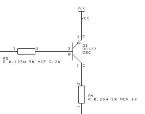
The LED power is controlled by using a PNP transistor (the 7-segments share a common anode). In this circuit the power is run through a single current limiting resistor. This will mean that numbers with few digits (for example, 1) will be displayed more brightly then those with a large number of segments (say 8). The final circuit would need to refined to have a current limiting resistor per segment or using a constant current driver. This component of the circuit looks like this:

Power control for a single 7-segment LED module.

The resistor R5 is connected to the output of the microcontroller and the output of R9 going through to the power pin on the 7-segment display.

Decoding the 7-segments

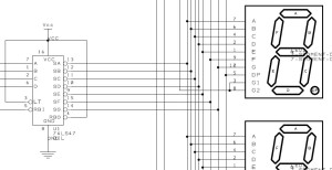
The decoding of the output from the microcontroller is performed by the 74LS47 chip. This is a dedicated decoder circuit for common anode 7-segment LED modules. The system takes a binary coded decimal number and then sinks the current from the appropriate segments of the display. The result is that the module will display the appropriate digit.

We will also take advantage of one final line, the RBI line. By turning this line on and off we can determine if the digit will display the digit 0 when the input to the decoder is zero. So why would we change this line? We we could fix the line so that a digit will always be displayed. So when the microcontroller wants to show 0 it will actually show either a blank display or 0000. The blank display is obviously not desirable as the user will not be able to determine if the display is showing 0 or if it is turned off. Showing four zeroes will give the user the correct information. A nicer solution is for the display to show a single zero when the microcontroller outputs 0.

The resulting decoder wiring looks something like the following:

7-segment decoder circuit

Where pins A, B, C and D will output the binary version of the digit to be displayed.

Full Circuit

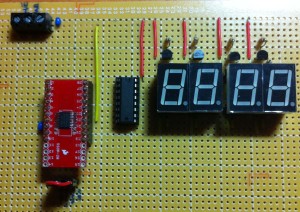
This PDF File contains the full circuit diagram for the proof of concept module. The fully assembled circuit looks like this:

Prototype Circuit

Software

In order to test the circuit we will write a small program which will start at 0 and count to 9999 before returning to 0 and starting counting again.

The first thing we need to do is to initialise the system. The following code resets the system clock source, configures the GPIO lines and then starts the timer which contain the code which will perform the multiplexing.

//
//  Initialise the clock
//
CLK_DeInit();
CLK_SYSCLKConfig(CLK_PRESCALER_CPUDIV1);                // CPU Prescaler = 1.
CLK_SYSCLKConfig(CLK_PRESCALER_HSIDIV1);                // Prescaler = 1, 16 MHz.
CLK_ClockSwitchConfig(CLK_SWITCHMODE_AUTO,              // Automatically switch
					  CLK_SOURCE_HSE,                   // Switch to internal timer.
					  DISABLE,                          // Disable the clock switch interrupt.
					  CLK_CURRENTCLOCKSTATE_DISABLE);   // Disable the previous clock.
//
//  Initialise GPIOs
//
GPIO_DeInit(GPIOC);
GPIO_Init(DIGIT0_BI_PORT, DIGIT0_BI_PIN, GPIO_MODE_OUT_PP_LOW_FAST);
GPIO_Init(DIGIT1_BI_PORT, DIGIT1_BI_PIN, GPIO_MODE_OUT_PP_LOW_FAST);
GPIO_Init(DIGIT2_BI_PORT, DIGIT2_BI_PIN, GPIO_MODE_OUT_PP_LOW_FAST);
GPIO_Init(DIGIT3_BI_PORT, DIGIT3_BI_PIN, GPIO_MODE_OUT_PP_LOW_FAST);
GPIO_Init(DIGIT_A0_PORT, DIGIT_A0_PIN, GPIO_MODE_OUT_PP_LOW_FAST);
GPIO_Init(DIGIT_A1_PORT, DIGIT_A1_PIN, GPIO_MODE_OUT_PP_LOW_FAST);
GPIO_Init(DIGIT_A2_PORT, DIGIT_A2_PIN, GPIO_MODE_OUT_PP_LOW_FAST);
GPIO_Init(DIGIT_A3_PORT, DIGIT_A3_PIN, GPIO_MODE_OUT_PP_LOW_FAST);
GPIO_Init(RBI_PORT, RBI_PIN, GPIO_MODE_OUT_PP_LOW_FAST);
//
//  Setup timer 2 to interrupt every 2048 clock pulses.
//
TIM2_DeInit();
TIM2_TimeBaseInit(TIM2_PRESCALER_2048,      // Interrupt every 2048 clock pulses.
				  1);                       // Period is one.
TIM2_ITConfig(TIM2_IT_UPDATE, ENABLE);      // Enable the overflow interrupt.
TIM2_Cmd(ENABLE);

The next thing we need to do is to look at displaying a digit. To do this we will turn off all of the digits and then convert the digit into binary outputting the value on the four pins connected to the 74LS47 decoder.

GPIO_WriteHigh(DIGIT0_BI_PORT, DIGIT0_BI_PIN);
GPIO_WriteHigh(DIGIT1_BI_PORT, DIGIT1_BI_PIN);
GPIO_WriteHigh(DIGIT2_BI_PORT, DIGIT2_BI_PIN);
GPIO_WriteHigh(DIGIT3_BI_PORT, DIGIT3_BI_PIN);
if (digit & 0x01)
{
	GPIO_WriteHigh(DIGIT_A0_PORT, DIGIT_A0_PIN);
}
else
{
	GPIO_WriteLow(DIGIT_A0_PORT, DIGIT_A0_PIN);
}
if (digit & 0x02)
{
	GPIO_WriteHigh(DIGIT_A1_PORT, DIGIT_A1_PIN);
}
else
{
	GPIO_WriteLow(DIGIT_A1_PORT, DIGIT_A1_PIN);
}
if (digit & 0x04)
{
	GPIO_WriteHigh(DIGIT_A2_PORT, DIGIT_A2_PIN);
}
else
{
	GPIO_WriteLow(DIGIT_A2_PORT, DIGIT_A2_PIN);
}
if (digit & 0x08)
{
	GPIO_WriteHigh(DIGIT_A3_PORT, DIGIT_A3_PIN);
}
else
{
	GPIO_WriteLow(DIGIT_A3_PORT, DIGIT_A3_PIN);
}
GPIO_WriteLow(port, pin);

The final statement will turn on the PNP transistor connected to the selected digit by connecting the base of the transistor to ground.

The final piece of code we need (before the main program loop) is the interrupt handler for the timer. This will turn off all of the power to the LED modules and then work out which digit to show and write the data to the 74LS47 decoder. This interrupt service routine can be found in the file stm8s_it.c. See previous STM8S post on interrupts for further information. Look for the following code in this file:

INTERRUPT_HANDLER(TIM2_UPD_OVF_BRK_IRQHandler, 13)
{
}

And replace with the following code:

INTERRUPT_HANDLER(TIM2_UPD_OVF_BRK_IRQHandler, 13)
{
    if (_currentDigit == 0)
    {
        DisplayDigit(_displayValue[0], DIGIT0_BI_PORT, DIGIT0_BI_PIN);
        GPIO_WriteHigh(RBI_PORT, RBI_PIN);
        _currentDigit++;
    }
    else
    {
        if (_currentDigit == 1)
        {
            DisplayDigit(_displayValue[1], DIGIT1_BI_PORT, DIGIT1_BI_PIN);
            if ((_displayValue[2] != 0) || (_displayValue[3] != 0))
            {
                GPIO_WriteHigh(RBI_PORT, RBI_PIN);
            }
            else
            {
                GPIO_WriteLow(RBI_PORT, RBI_PIN);
            }
            _currentDigit++;
        }
        else
        {
            if (_currentDigit == 2)
            {
                DisplayDigit(_displayValue[2], DIGIT2_BI_PORT, DIGIT2_BI_PIN);
            if (_displayValue[3] != 0)
            {
                GPIO_WriteHigh(RBI_PORT, RBI_PIN);
            }
            else
            {
                GPIO_WriteLow(RBI_PORT, RBI_PIN);
            }
                _currentDigit++;
            }
            else
            {
                DisplayDigit(_displayValue[3], DIGIT3_BI_PORT, DIGIT3_BI_PIN);
                GPIO_WriteLow(RBI_PORT, RBI_PIN);
                _currentDigit = 0;
            }
        }
    }
    TIM2->SR1 = (uint8_t) (~(uint8_t) TIM2_IT_UPDATE);  // Clear the interrupt.
}

One interesting thing to look at is the setting of the RBI_PORT. Note that this is set to high for the first digit (i.e. rightmost digit) and low for all of the other digits. This is the piece of magic which ensure that we always display a digit for zero in the rightmost digit but only display a value for no zero digits on the remaining three digits.

If this were to be taken forward then the code above would need to be optimised to ensure that the ISR completed in the shortest time possible.

Now we have all of the elements in place we can start to write our main program loop. The code will loop from 0 to 9999 displaying each digit and the restarting the count. The individual digits will be put into an array of four integers, one for each LED in the display. This gives us the following code:

enableInterrupts();                         // Make sure interrupts are enabled.
int value = 0;
while (1)
{
	_displayValue[0] = value % 10;
	_displayValue[1] = (value / 10) % 10;
	_displayValue[2] = (value / 100) % 10;
	_displayValue[3] = (value / 1000) % 10;
	if (value == 9999)
	{
		value = 0;
	}
	else
	{
		value++;
	}
	//
	//  Now delay otherwise we'll be counting too fast for anything
	//  to appear on the display.
	//
	for (int outerDelay = 0; outerDelay < 5; outerDelay++)
	{
		for (int delay = 0; delay < 0xffff; delay++)
		{
			nop();
		}
	}
}

The full source code for this project can be downloaded here.

Conclusion

This was an interesting project to put together and took about a day to work out and get everything working. To take this further would take a lot more work, many times the amount already put into the project. As two other groups are working on similar ideas I have decided to archive this for now and move on to other projects.

Software for the LED Cube

Sunday, March 18th, 2012

So you’ve built is and now we need some software to run it. To do this we are going to need to perform two tasks at the same time:

  • Calculate what we are going to display in the cube
  • Run the display

Multithreading is used in order to achieve this. The program has one thread which does nothing but cycle through each layer one by one shifting the data for the layer into the shift registers and then turning the layer on.

The second thread prepares the next item to be displayed and then passes this on to the cube to display.

LEDCube Class

This is a relatively simple class having a single constructor and two methods. The constructor sets the scene for us and makes sure everything is ready to use:

public LEDCube()
{
    config = new SPI.Configuration(SPI_mod: SPI.SPI_module.SPI1,
                                   ChipSelect_Port: Pins.GPIO_PIN_20,
                                   ChipSelect_ActiveState: false,
                                   ChipSelect_SetupTime: 0,
                                   ChipSelect_HoldTime: 0,
                                   Clock_IdleState: true,
                                   Clock_Edge: true,
                                   Clock_RateKHz: 100);

    spi = new SPI(config);
    buffer = new byte[64];
    for (int index = 0; index < buffer.Length; index++)
    {
        buffer[index] = 0;
    }
}

The buffer contains the data we are going to be showing in the cube.

The next two methods perform the work or updating and displaying the buffer. We need to be careful that the buffer is not updated whilst we are trying to update the display.

public void UpdateBuffer(byte[] newValues)
{
    lock (buffer)
    {
        for (int index = 0; index < buffer.Length; index++)
        {
            buffer[index] = newValues[index];
        }
    }
}

The lock statement helps us to achieve this by locking the buffer so we can copy data into it and also stop the display method from trying to read the buffer and show the data.

The display method is a little longer:

public void DisplayBuffer()
{
    while (true)
    {
        lock (buffer)
        {
            byte[] displayData = new byte[8];

            for (int row = 0; row < 8; row++)
            {
                int offset = row * 8;
                for (int index = 0; index < 8; index++)
                {
                    displayData[index] = buffer[offset + index];
                }
                enable.Write(true);
                bit0.Write((row & 1) != 0);
                bit1.Write((row & 2) != 0);
                bit2.Write((row & 4) != 0);
                spi.Write(displayData);
                enable.Write(false);
            }
        }
    }
}

This method again uses the lock statement to lock the buffer. This means we cannot update the buffer until a full cube of data has been displayed. The method takes a block of 8 bytes representing a layer and then writes this to the shift registers using SPI. Note that the spi.Write is embedded in the writes to the enable line. This ensures that all of the layers are turned off whilst we are updating the shift registers.

Wrapping all of this in the LEDCube class means that we now have a very simple class where we can spawn the DislpayBuffer method into it’s own thread. So off to out Main program. We are going to need an instance of the cube and a buffer to hold the next “frame” we wish to display.

private static LEDCube cube = new LEDCube();
private static byte[] nv = new byte[64];

The first thing we do when entering the main program is to set all of the values in the buffer (set them to zero) and to start the display thread going:

ClearCube();
Thread display = new Thread(new ThreadStart(cube.DisplayBuffer));
display.Start();

ClearCube does just that, sets the values to zero and then calls the cube Update method to copy this zeroed buffer into the cube buffer.

The next line spawns a new thread which runs the DisplayBuffer method and the following line starts it.

At this point we have two threads, the main program loop and the display thread. We can now perform calculations in the main program loop and call cube.UpdateBuffer when we have new data to display.

So how about something to display, a little rain perhaps:

private static void AddDrops(int count, int plane = -1)
{
    for (int drops = 0; drops < count; drops++)
    {
        bool findingSpace = true;
        while (findingSpace)
        {
            int x = rand.Next() % 8;
            int y = rand.Next() % 8;
            int z;

            if (plane == -1)
            {
                z = rand.Next() % 8;
            }
            else
            {
                z = plane;
            }

            int position = ( z * 8 ) + y;
            byte value = (byte) ((1 << x) & 0xff);
            if ((nv[position] & value) == 0)
            {
                nv[position] |= value;
                findingSpace = false;
            }
        }
    }
}

private static void Rain(int noDrops, int cycles)
{
    ClearCube();
    AddDrops(noDrops);
    cube.UpdateBuffer(nv);
    for (int currentCycle = 0; currentCycle < cycles; currentCycle++)
    {
        int bitCount = 0;
        for (int plane = 0; plane < 8; plane++)
        {
            byte value = 1;
            for (int bit = 0; bit < 8; bit++)
            {
                if ((nv[56 + plane] & value) > 0)
                {
                    bitCount++;
                }
                value <<= 1;
            }
        }
        for (int plane = 7; plane > 0; plane--)
        {
            for (int currentByte = 0; currentByte < 8; currentByte++)
            {
                nv[(plane * 8) + currentByte] = nv[( (plane - 1) * 8 ) + currentByte];
            }
        }
        for (int b = 0; b < 8; b++)
        {
            nv[b] = 0;
        }
        AddDrops(bitCount, 0);
        cube.UpdateBuffer(nv);
        Thread.Sleep(75);
    }
}

AddDrops simply adds a specified number of rain drops to the buffer. It also makes sure that if asked for 10 it will always add 10 by checking to see if one exists in the location it wanted to use.

Rain adds the specified number of drops to the buffer, shows the drops and then moved them all down by one plane. Before doing this it counts how many drops are going to fall out of the cube. After all the drops have moved down one plane it adds the drops which have disappeared out of the bottom of the cube back in at the top in random positions.

We can display this by adding this to the main program:

while (true)
{
	Rain(10, 60000);
}

The full source code to this project is current hosted on Codeplex.

Conclusion

Hope that you enjoy trying out this project but be aware that it takes time. This consumed a lot of my spare time for about three weeks. There are still some tasks to complete

  • Power supply
  • A case
But the main stuff is working.

I have not covered the power regulation but you should make sure that you have a regulated 5V DC power supply capable of about 2A – but more would be better. I did actually add my own regulator to this project but it got very hot when the cube was fully lit. Beware – make sure you have a stable supply capable of supplying enough juice.

The Controller Board

Sunday, March 18th, 2012

Having a cube of LEDs is of little use without a controller board. As previously mentioned, all 512 LEDs can be controlled from just 7 lines from the Netduino Mini. As you will have seen during the testing, we can turn on any LED by connecting the anode to a positive supply and the entire layer in which it sits to ground.

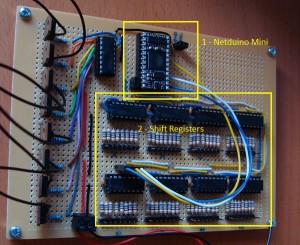
The positive supply is a relatively simple thing to achieve and our good friend the 74HC595 shift register will help us there. Connecting to ground requires a little more work but this is achieved using the 74HC238 and a bank of transistors. At the end of this process I had the following board:

Annotated Controller Board

So, a quick walk around the board. Box one contains the Netduino Mini. The two connectors to the bottom left of the board allow the Mini to be connected to the computer – they are the Mini’s COM1 connections. The two connectors at the top right are for the ground and the 5V from my USB – FTDI connector. Only ground is connected, the other connector allows me to stop the 5V lead from flying around and touching something it shouldn’t.

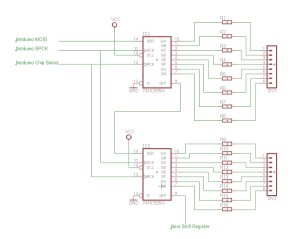
Box 2 contains the bank of 8 x 74HC595s, current limiting resistors and a connector to allow a ribbon cable to be connected the cube to the controller. These will determine which of the LEDs received power. Each of the shift registers will control one row of LEDs, 8 rows need 8 registers. So the shift registers can control 64 LEDs at once.

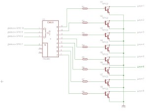
The remainder of the electronics on the board determine which layer will be connected to ground. The 74HC238 takes four lines from the Mini. Three of the lines represent a binary number 0-7, the fourth line is an output enable line. The decoder takes the number and switches on one of one of the output lines. This is in turn connected to the base of a TIP122 transistor. Applying power to the base allows the layer the transistor is connected to connect to ground.

So all is in place to use persistence of vision to be used to give the appearance that the cube is permanently switched on. Starting with the cube switched off we load the shift registers with the data for layer 0. We then load the 74HC238 with 0 and enable the output. This will turn on the transistor for layer 0 which will allow current to flow through the LEDs in layer 0. We then turn the cube off by disabling the output of the 74HC238 and repeat for layer 1 and so on.

Shift Registers

A little more repetition – don’t you just love it. The eight shift registers are wired together in a cascade with the shifted output of one register forming the input of the next. By connecting eight together we can control 64 outputs.

The basic connections for the shift registers is as follows:

Schematic for the Cascaded Shift Registers

This needs to be repeated until all eight of the registers are connected as in the above diagram. In the controller board diagram the serial data in wires are blue, the clock wires are white and the enable wires are yellow.

Note that a 100nF ceramic capacitor is connected between power and ground and one is placed by each IC as close to the IC as possible.

The current limiting resistors for this project were selected to keep the current per LED at 25mA per LED. The nearest value actually puts this at 26mA per LED. Multiplying this up means that a layer when all of the LEDs are switched on will draw 1.6A. The maximum output current rating per pin on the 74HC494 is 35mA so we are getting close to the limit per pin.

Layer Switching

Layer switching is achieved by connecting a layer to ground through a TIP122 transistor. This should be capable of sinking 2A which is greater than the 1.6A which we could theoretically need to sink if all of the LEDs on a layer are switched on. The 74HC238 selects which layer is connected to ground – or in fact none of them may be connected if the output from the 74HC238 is disabled. The circuit diagram for this part of the controller looks as follows:

Layer Selection Schematic

Again, a 100nF capacitor is placed across power and ground for this IC.

Connecting the Controller to the Cube

The collector for each of the TIP122’s should be connected to a different layer. I connected mine with layer zero being the top layer.

Each of the shift registers should be connected to one row of LEDs. I connected mine with bit zero at the right of the cube. This was done with one of the female connectors (to fit the male connector on the controller board) and some ribbon cable.

The result of these two wiring decisions was a rather odd co-ordinate system. You may decide to use something more conventional.

Adding the Netduino Mini

The Netduino Mini connections have already been noted on the above schematics.

Making the Cube

Sunday, March 18th, 2012

For the majority of June I was working on making the LED cube featured in my previous post. The next few posts will cover making the cube and writing the software which controls it.

The initial post of the cube working first appeared on the Netduino forums in early July. As you can see, it received some good responses.

This project will require the following materials:

Description Quantity
LEDs (use which ever colour floats your boat – I went for blue) 512
74HC595 Shift Registers 8
74HC238 3 to 8 line decoder 1
Netduino Mini 1
16 Pin DIL Socket 9
24 Pin DIL Socket (0.6″) 1
TIP122 NPN Transistor 8
100nF Ceramic Capacitor 10
2.2K Resistor 8
68 Ohm 0.25W Resistor (you may need to change these depending upon the LED you choose) 64
8 Way Single Row Socket 8
36 Way Header Strip (Straight) 2
2 Way Single Row Socket 2
2 Way PCB Mount Terminal Connector 1
8 Way Ribbon Cable 2.5 metres
Wire and connectors Miscellaneous
Pad board 160 x 115 Hole 1
Hex PCB spaces, M3 threaded and M3 screw 4

As well as the above you will need the following items:

  • 5V Power capable of delivering 2A;
  • Solder – I used about 15 metres over the life of this project;
  • Wood to make a template.

As well as the physical items you will need a fair amount of patience and good attention to detail. There are a lot of repetitive tasks in this project. The method is detailed in the three articles listed at the head of this article.

Making a Cube of LEDs

Sunday, March 18th, 2012

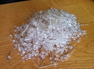
This is probably the most time consuming part of the project requiring a lot of patience, testing and a 30cm x 30cm piece of wood. Seriously, you’ll need a piece of wood. Here we are going to convert this:

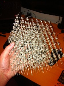
Into this:

Working out the Dimensions of the Cube

The exact dimensions of the cube will depend upon the length of the legs on the LEDs. The legs will be soldered together with the cathodes of the LEDs forming a horizontal plane and the anodes connecting the layers vertically.

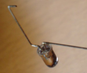
Take one of the LEDs and bend the cathode at a point as close to the body of the LED as possible. The cathode should be at 90 degrees to the anode and parallel to the flat base of the LED. Now bend the top 3mm of the leg of the anode through 90 degrees. You are aiming for something which looks like this:

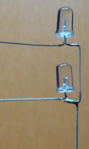
In the final cube we want all of our LEDs to be above each other. If we don’t then each layer will be slightly offset from the on beneath it. We won’t have a cube more of a leaning tower. So the final act of manipulation for the LED is to bend the anode of the LED slightly out from the body of the LED and then to straighten the anode again. The effect should be that the 3mm at the end of the anode should be enough to place the LEDS above each other. When they are connected in the cube they should look like this:

Layer Template

Measure the distance from the centre of the now horizontal cathode to the end of the leg and subtract about 2mm. This will tell you how far apart the LEDs are in the horizontal plane. The 2mm will be used to overlap with the neighbouring LED and will be used to connect the cathodes. Now this is where the wood comes in. You need to drill a grid of holes 8 x 8 which are each this measured distance apart. You will end up with a template in which you can place the LEDs in each layer making soldering easier.

The holes in the template must be small enough to hold the LED firmly but not too firm. The LEDs will need to be removed later without placing too much strain on the soldered joints.

Building the Layers

So now let’s get the soldering iron warmed up and on with the first layer. Take 8 of the LEDs and place them along the top row with the cathodes all pointing to the right (or left if you prefer). The cathodes of the 7 LEDs to the left will overlap slightly with the LED to the right. The rightmost cathode will go off into space. Solder the cathodes together. Congratulations, you now have a line of LEDs.

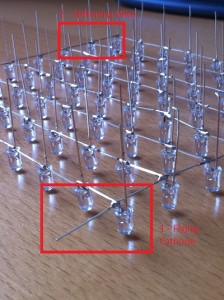
Now let’s add the remaining LEDs in the layer. I started on the left as I hold the soldering iron in my right hand. Take another 7 LEDs and place these under the top row down the far left column. Again the cathodes should be overlapping. Solder these together. Repeat with the remaining columns. At this point you should have a horizontal row of LEDs connected together with 8 strings of 7 LEDs hanging from it. Eventually you should have something looking like this:

Now test the layer. Simple enough, you just need a power supply and a current limiting resistor. For the LEDs I had chosen a 5V supply fed through a 68 Ohm resistor is adequate. Connect ground to the cathode of the LED which is flying off into space (remember, it’s on the top row, to the right). Now touch each leg of the LEDs in turn with the positive output of the supply (through the current limiting resistor of course). The LEDs should light up and as you touch the anode.

One final bit of soldering is to add a stiffening wire to the layer. Cut and strip a piece of wire. The wire should be long enough to cross the entire layer. Now solder the stiffening wire to the cathodes along the bottom of the layer. See the image above. One thing to note here is that although one piece of wire is sufficient, adding one or two more would not harm.

At this point you will have one complete layer. Time to remove it from the template. This should be done carefully so that you do not put too much stress on the joints. Lifting it up gently with a screwdriver should help. Do not be in a hurry, gently freeing the LEDs first may help. Put this layer to one side and repeat another 7 times.

Connecting the Layers

Now that we have all of the layers built I suggest that they are tested once again. This repeated test may save you pain later. Just imagine how difficult it will be to fix a bad joint in the middle of the cube. We are just checking that the LEDs are still connected and none of the joints have been broken removing the layers from the template.

Now drop one of the layers back into the template. What we now need to do is to place a second layer on top of this one so that the anodes of the layer in the template touch the anodes of the LEDs in this layer. Once in place we need to solder the anodes together – good game, good game. I had the advantage of having a few clamps which could be adjusted vertically as well as horizontally. I would imagine that cardboard (or wood) shaped to the correct height should help support the layers. Remember that whatever you use you will need to be able to remove it without damaging the cube.

Now you have the layer supported, solder the anode of the LEDs in the top layer to the anode of the LED in the layer directly beneath it. Once this has been done – test. Connect the cathode of the bottom layer to ground and touch each of the legs on the top layer in turn with the +ve supply (going through the current limiting resistor). The LED on the bottom layer should light. Move the cathode to the top layer and repeat the test, this time the LED on the top layer should light.

Repeat adding the remaining layers. Just for safety, I would test every layer in the cube as it is built up. This repeated testing sounds like a big overhead but trust me it’s worth it.

So at this point you should now have a cube and if you are like me, lost two days of your life in pursuit of happiness and all that is good in life.

LED Cube – How to Build One

Tuesday, November 8th, 2011

Coding4Fun have just published my article on how to build a 512 LED cube controlled by a Netduino Mini.

Cascading TLC5940 LED Drivers

Wednesday, November 2nd, 2011

A while ago I created a circuit and some code to control the TLC5940 LED driver using a Netduino Mini. This chip allowed the programmer to control 16 LEDs using a serial interface. In the conclusions I noted that it should be possible to control two or more of these chips by cascading the serial output from one chip into another. This article discusses the additional hardware required along with the software to control up to 32 LEDs using two of these chips linked together.

It is assumed that you have read and understood the previous article before you proceed further.

Hardware

Linking two of these chips is a relatively simple affair and requires the LEDs you wish to control and only 1 additional component, namely a 2K2 ohm resistor, and some additional wire (assuming you are using breadboard).

Starting with the simplest part, the 2K2 ohm resistor connects the IREF pin on the second TLC5940 to ground. This sets the reference voltage for the LEDs connected to the second TLC5940.

The next part of the problem is to connect the two chips together. This is achieved by connecting the following pins:

TLC5940 (1)TLC5940 (2)
SCLKSCLK
BLANKBLANK
XLATXLAT
GSCLKGSCLK
VPRGVPRG
SOUTSIN
XERRXERR

DCPRG on TLC5940 is connected to Vcc as it is on the first driver chip and the LED controller pins connected to the appropriate LEDs.

This PDF (PWMLEDControlv0.03.pdf) contains the full circuit diagram showing the connections required.

Software

Now we have the additional LEDs in the circuit we will need to be able tell the software driver for the chips how many LEDs we want to control and then be able to control the brightness of the LEDs. In order to do this an additional parameter was added to the constructor numberOfLEDs. This parameter allows the system to work out how many TLC5940’s should be connected together. Once we have the number of chips calculated we can then work out the size of the buffers for the Dot Correction and the Grey Scale data.

The class uses two buffers for both the Dot Correction and the Grey Scale data. This may seem superfluous but doing this allows two different modes of operation:

  • Basic – The LEDs can be controlled using an interface which is simpler to use but is slower.
  • Fast – This mode is faster but requires the programmer to perform some of the tasks in the driver. The assumption here is that the programmer will have more understanding of the data which is changing and can therefore write more optimised code.

For the moment we will be discussing the basic mode. In this mode, the software driver hides much of the implementation and the user only really needs to perform three tasks:

  • Construct a new instance of the software driver.
  • Set the brightness of the LEDs (only the lower 12 bits are used).
  • Tell the driver to output the data to the TLC5940 chips.

Constructor

Making a new instance of the class in it’s most basic form is simply a case of telling the constructor how many LEDs you wish to control. In this case we have two TLC5940s connected together and so we have 32 LEDs:

Tlc5940 leds = new Tlc5940(numberOfLEDs: 32);

You can of course use the additional parameters to define the pins used for the various control signals or just use the defaults.

Setting a LED

The class contains a method which overloads the array indexing operator. Setting the brightness for a LED is simply a case of using this operator as follows:

leds[10] = 767;

This will set the brightness of LED 10 to the value 767.

An important note here is that the LEDs are numbered from 0 to 15 on the TLC5940 connected to the Netduino Mini, 16 to 31 on the next LED in sequence and so on.

Lighting the LEDs

The final piece of the puzzle is to output the data to the series of TLC5940s connected to the Netduino Mini. This is achieved by calling the Display method in the Tlc5940 class.

Source Code

The source code for the controller class and a simple main program can be found here (CascadedTLC5940.zip).

Conclusion

The work with this chip has not yet finished as there are still some points which need addressing in order to round off this class:

  • Dot Correction – this current outputs all 1’s and so there is no fine control for any of the outputs.
  • Error Detection and Status Information – It is possible to detect two types of errors and retrieve the status information from the TLC5940. This needs implementing.

One final item which needs addressing is to round off the code once these final feature have been implemented. A topic for another day.