TLC5940 16 Channel PWM Driver
I have recently been working with the TLC5940 LED Driver chip. This provides 16 PWM outputs which can be used to drive common anode LEDs and I suspect motors etc. For the moment I will be using it to drive 16 LEDs to prove the principle and work out how to interface the chip to the Netduino Mini.
The article and code contained here should allow the creation of a circuit capable of doing the following (and a whole lot more):
Objective
The objective of this exercise is to use the TLC5940 to control 16 LEDs under the control of the Netduino Mini. This will require the following to be developed:
- Timer circuit to control the grey scale output.
- Control signals and reference voltage to control the output of the TLC5940
- Control logic and software for the Netduino Mini
A description of PWM and how it works is assumed. If you require more information then you can check out the Wikipedia article on PWM.
Timer (Clock) Circuit
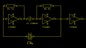
The TLC5940 uses an external timing signal to control the 16 grey scale outputs to the LEDs. This signal can be as high as 30 MHz. The design presented here uses an 8 MHz crystal / resonator. When I was developing the circuit I have little knowledge of how to build the timer and so used a NE555 configured as a 40 kHz astable oscillator. This was crude but was good enough to start the project. The final design uses an oscillator circuit from a document recommended by Mario on the Netduino forums. You can read the original post here. Mario recommended circuit 1d which is the one I finally used:
The final inverter is not really necessary but the chip contains 6 inverters and I was only using two so I fed the output from the timer through an final inverter. This had the effect or producing a squarer signal – although the final signal is still slightly rounded.
In the final circuit I actually used a resonator. I simply dropped this in place of the crystal connecting the outer two pins to the logic gates and the centre pin to ground.
Control Signals
As well as the clock signal, the TLC5940 requires several control signals to determine how the chip should treat the grey scale data. This section looks at each signal and describes its function.
BLANK (Pin 23)
This pin determines the output state of the TLC5940. When this pin is high the outputs are turned off. Setting the pin low turns the outputs back on. More importantly, it changes the internal counter for the PWM control and resets the counter to 0. It is to this counter to which we now turn out attention.
The TLC5940 uses 12 bits to determine the output level for the LEDs connected. Each LED is controlled independently and the full array of 12 bits requires a total of 192 bits (12 bits x 16 LEDs) of data to determine the output levels for the LEDs. The 12 bits for each LED gives a total of 4096 (remember this number, we’ll be using it later) levels for each LED (0 to 4095 inclusive). The TLC5940 uses this data and the current counter to determine the output state of each OUT pin.
Setting BLANK to high and then low causes the counter to be set to zero. An incoming clock pulse causes the counter to be incremented by 1. The chip then turns on all of the outputs which have a greyscale value which is non-zero. Each subsequent pulse cause the chip to do the following:
- Increment the counter
- For each output compare the counter with the greyscale value for the output pin. If the value is greater than the counter then turn the output on, else turn the output off.
This process repeats until the internal counter reaches 4095 at which point the process stops and the outputs are effectively turned off (the counter value is greater than or equal the output value for the LEDs). This point is important as providing only one pulse to BLANK and a series of 4096 (or more) clock pulses makes this a one time only output. The LED on each output lights for the specified duty cycle and then turns off.
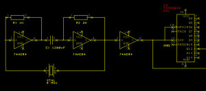
The trick here is to ensure that a BLANK pulse is generated for every 4096 greyscale clock pulses. This is achieved by attaching the output from the timer circuit to both the greyscale clock on the TLC5940 and a divider circuit. The divider counts 4096 clock pulses and then outputs a new BLANK signal to the TLC5940 effectively restarting the counting process. So the modified clock circuit looks something like this:
The clock signal is split and one connection to the GSCLK (grey scale clock) pin on the TLC5940, the other connection is to the clock inputs of a 14-bit counter/divider (74HC4060). The divider counts the clock pulses and sets the output pins of the chip to represent the current value of the counter. The counter is reset once it reaches the maximum value and the whole process restarts. The counter does not output the lower three bits but this is not an issue for us as we are interested in counting to 4096. We can use the output from bit 12 (2 ^ 12 = 4096) as a BLANK signal for the TLC5940. So for the first 4095 pulses the TLC is setting the outputs according to the values held for each pin. When the counter reaches 4096, the TLC stops displaying data but then a BLANK pulse is received from the divider. This then restarts the whole process. The result, we have the outputs continuously cycling the the LEDs on for the required duty cycle.
One final point about the BLANK signal. This could be used by the microcontroller which is controlling the circuit to turn off the outputs. To allow for this, the output from the divider is ORed with the BLANK signal coming from the microcontroller. The output from the OR gate is passed on to the TLC5940.
VPRG (pin 27)
This signal determines the type of data being transmitted to the TLC5940.
When VPRG is high the chip expected 96 bits of data for the Dot Correction (DC) registers. The DC registers allow the controller to scale the output current supplied at each output pin. This is covered later in this article.
When VPRG is low, the TLC5940 expects 192 bits of data for the grey scale registers.
XLAT (pin 24)
A low-high pulse on this pin latches the data received from the microcontroller into the DC or the GS registers. The data is latched on the rising edge (i.e. low to high) of the XLAT signal.
DCPRG (pin 19)
This pin is not used in this circuit and to connected to Vcc
IREF (pin 20)
This pin can be used to set the maximum current output on each of the output pins. This is done by connecting the pin to ground through a resistor. The value of the resistor is determined by the following calculation:
R = (1.24 / Imax) * 31.5
Where Imax is the maximum current to be supplied. The value of 1.24 is the reference voltage on the IREF pin.
For the LEDs I am using I want a maximum current of about 26mA. This gives a resistor value of 1502 ohms, so a 1k5 resistor should do here.
XERR (pin 16)
This pin is an output from the TLC5940 and can be used to report when an error is detected. This pin is not used in this project and is connected through a 10K pull-up resistor to Vcc.
Grey Scale and Dot Correction
The TLC5940 uses a value in the range 0-4095 to represent the duty cycle for each of the outputs. This gives an effective brightness for each LED given by the following calculation:
Percentage brightness = (Grey Scale value for output N / 4095) * 100
The dot correction reduces the current flowing through the output pins. This can have two effects, it can be used to adjust the current to bring it in range for a specific LED or it can be used to fine tune the output current for an output pin. This can effectively reduce the brightness of a LED. The change in maximum current for a pin is given by the following calculation:
Iout = Imax * (Dot correction value for pin N / 63)
Where Imax is set using the resistor connected to the IREF pin (discussed above).
Final Circuit
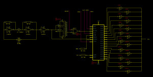
The final circuit looks like this:
Controlling the Chip
The whole circuit is controlled using a Netduino Mini. The four pink control lines in the above circuit are used by the Netduino Mini to control the TLC5940.
| Pin Name | Description |
| MOSI / SIN | Serial data output from the Netduino Mini (pin 14 on the Netduino Mini) |
| SPCK / SCLK | Clock signal for the serial data (pin 16 on the Netduino Mini) |
| XLAT | Data latch signal. This could be connected to the chip select although in the initial implementation this is broken out to it’s own pin. |
| VPRG | Determine the programming mode for the TLC5940. High: Dot Correction data is being loaded. Low: Grey Scale data is being loaded. |
| BLANK | Turn the outputs (LEDs) on or off. High: Outputs off. Low: Outputs on. |
The application encapsulates the TLC5940 functionality in a single class Tlc5940. This project only deals with one chip controlling 16 outputs (even though several can be linked together). The class only exposes 2 methods:
- Constructor
- Display
Constructor
The constructor sets up the system to use the SPI interface and takes parameters to determine which additional control pins should be used.
Display
The display method takes two parameters, one for each of the dot correction data and one for the grey scale data.
The main program contains a small demonstration of the functionality of this class and the TLC5940 chip. It slowly fades in 16 LEDs from off to full brightness and then fades them out to the off state again. This is repeated in a loop forever. For an example of the output see the video at the top of this article.
The code is pretty well commented and so further discussion is not provided here.
You can find the source code here (TLC5940.zip).
Conclusion
This article is really a starter for this chip as there is a whole lot more which is possible. There are a number of areas where I would like to expand both the code and the circuit, namely:
- Resetting the counter when it reaches 4096. At the moment this runs on until it reaches the maximum value.
- Use the dot correction values to allow different LEDs to be used on each pin. Different LEDs have different forward currents and this can be fine tuned using the dot correction data to allow the maximum brightness to be achieved by each individual LED.
- Look at using the CS pin on the SPI interface for the BLANK signal from the Netduino Mini to the TLC5940.
- Add some error checking code to check if the TLC5940 has detected any errors.
- Link two or more TLC5940’s together.
Adding these features will make this class more rounded and fully encapsulate the feature set offered by this circuit.
Tags: Electronics, LED, Netduino
Saturday, October 8th, 2011 at 6:52 am • Electronics, Netduino • RSS 2.0 feed Both comments and pings are currently closed.


