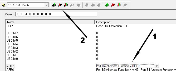
This post was supposed to be about controlling an LED panel using SPI on the STM32. It soon became apparent that SPI on the STM32 was a topic of it’s own and so the hardware component of the post, the LED panel, will have to wait for another day.
In this post we will aim to achieve the following:
- Use SysTick to trigger regular events
- Send data over SPI by polling
- Use interrupts to send data by SPI
- Combine SPI and DMA to send data over SPI
So let’s start with the trigger/heartbeat.
Heartbeat
The heartbeat will allow us to perform tasks at regular intervals, say 1ms, and by toggling a pin we can also determine if the processor is still “alive”.
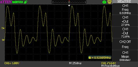
For a simple heartbeat we can use the SysTick timer. This built in timer can be configured to generate an interrupt. The handler has it’s own entry in the interrupt vector table. It is theoretically possible to calibrate this timer to trigger at an accurate period. For the purpose of this problem we will not really need high accuracy and so will simply turn on the timer.
Setting this timer running requires only two lines of code, encapsulating this into an initialisation method gives us the following:
//
//    Initialise SysTick.
//
void InitialiseSysTick()
{
    RCC_ClocksTypeDef RCC_Clocks;
    //
    //    Setup the system tick for the heartbeat.
    //
    RCC_GetClocksFreq(&RCC_Clocks);
    SysTick_Config(RCC_Clocks.HCLK_Frequency / 1000);
}
The SysTick_Config method sets up the SysTick timer. The timer works by loading the counter with a Load value. The counter then starts to count down from the load value each tick of the clock. When the counter reaches zero it is reloaded and the whole process starts again. It is possible to generate an interrupt (SysTick_Handler) when the counter reaches zero.
The expression RCC_Clocks.HCLK_Frequency / 1000 is the counter reload value. It is important to note that the reload value is a 24-bit unsigned long and so this has a maximum value of 0xffffff. In this case the load value is 0x29040, well within the specified range. This value will give 1000 interrupts per second, i.e. an interrupt every 1ms.
Now we have a 1ms interrupt we need to determine if this interrupt is being triggered. The simplest way of doing this is to toggle one of the GPIO pins. First thing to do is to select a pin and then initialise the port. Selecting PA1 we can modify the InitialiseSysTick code above to the following:
//
//    Initialise SysTick.
//
void InitialiseSysTick()
{
    GPIO_InitTypeDef GPIO_InitStructure;
    RCC_ClocksTypeDef RCC_Clocks;
    //
    //  Initialise the peripheral clock.
    //
    RCC_AHB1PeriphClockCmd(RCC_AHB1Periph_GPIOA, ENABLE);
    //
    //  Initialise the heartbeat GPIO port.
    //
    GPIO_InitStructure.GPIO_Pin = GPIO_Pin_1;
    GPIO_InitStructure.GPIO_Mode = GPIO_Mode_OUT;
    GPIO_InitStructure.GPIO_OType = GPIO_OType_PP;
    GPIO_InitStructure.GPIO_Speed = GPIO_Speed_50MHz;
    GPIO_InitStructure.GPIO_PuPd = GPIO_PuPd_NOPULL;
    GPIO_Init(GPIOA, &GPIO_InitStructure);
    //
    //    Setup the system tick for the heartbeat.
    //
    RCC_GetClocksFreq(&RCC_Clocks);
    SysTick_Config(RCC_Clocks.HCLK_Frequency / 1000);
}
The next task is to add the SysTick interrupt handler. Opening the startup_stm32f4xx.c file you will find the following line:
#pragma weak SysTick_Handler = Default_Handler
This statement defines the SysTick_Handler and points the handler to the Default_Handler. The weak attribute allows the developer to override this handler and provide their own interrupt handler. In our case we want the handler to toggle PA1. This gives the following code:
//
//    System tick handler.
//
void SysTick_Handler(void)
{
    //
    //    Generate a heartbeat.
    //
    GPIOA->ODR ^= GPIO_Pin_1;
}
All of the above code is placed in a file SysTick.c and an appropriate header file created. Our main program file is:
#include "SysTick.h"

//
//    Initialise the system.
//
void Initialise()
{
    InitialiseSysTick();
}

//
//    Main program loop.
//
int main()
{
    Initialise();
    while (1);
}
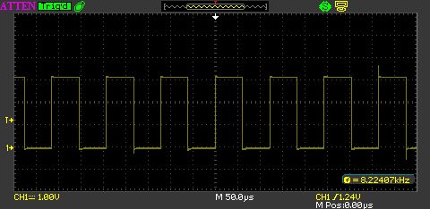
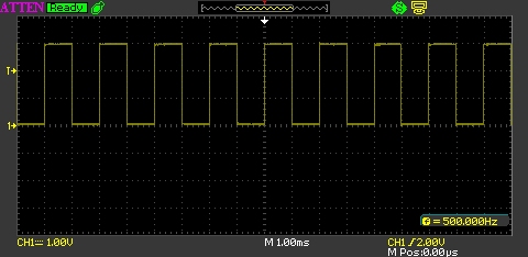
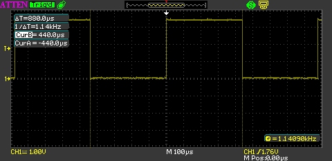
Putting this into a project, compiling and running results in the following output on the oscilloscope:
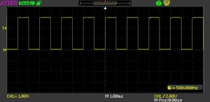
500Hz Square Wave
As you can see, we have a 500Hz square wave indicating that PA1 is being toggled 1,000 times per second.
Polled SPI
Polled SPI will use the various registers associated with the SPI feature to determine if the SPI data transmission has completed. You can also use interrupts, a subject we will come to later.
The first things we need to do is to configure the pins required to support SPI. For conventional SPI we need four pins:
- MOSI (PA7)
- MISO (PA6)
- SCLK (PA5)
- Chip select (PE6)
One change we will make is to move the heartbeat from Port A to Port E (PE5) and keep Port A for the SPI function. Abstracting the GPIO initialisation out to it’s own files gives the following header file:
//
//    Include file for the GPIO methods.
//
//    Copyright 2014 Mark Stevens
//
#include "stm32f4xx_rcc.h"
#include <stm32f4xx_gpio.h>


#ifndef _SPI_H_
#define _SPI_H_

#ifdef __cplusplus
extern "C"
{
#endif

void InitialiseGPIO();

#ifdef __cplusplus
}
#endif

#endif
and the code file:
//
//    GPIO methods.
//
//    Copyright 2014 Mark Stevens
//
#include "GPIO.h"

//
//    Initialise the GPIO ports setting up the clocks.
//
void InitialiseGPIO()
{
    GPIO_InitTypeDef GPIO_InitStructure;
    //
    //  Initialise the peripheral clocks.
    //
    RCC_AHB1PeriphClockCmd(RCC_AHB1Periph_GPIOA, ENABLE);
    RCC_AHB1PeriphClockCmd(RCC_AHB1Periph_GPIOE, ENABLE);
    //
    //    Configure pins used by SPI1:
    //        PA5 = SCLK
    //        PA6 = MISO
    //        PA7 = MOSI
    //
    GPIO_InitStructure.GPIO_Pin = GPIO_Pin_7 | GPIO_Pin_6 | GPIO_Pin_5;
    GPIO_InitStructure.GPIO_Mode = GPIO_Mode_AF;
    GPIO_InitStructure.GPIO_OType = GPIO_OType_PP;
    GPIO_InitStructure.GPIO_Speed = GPIO_Speed_50MHz;
    GPIO_InitStructure.GPIO_PuPd = GPIO_PuPd_NOPULL;
    GPIO_Init(GPIOA, &GPIO_InitStructure);
    //
    //    Configure the Port E:
    //        PE6 - SPI chip select pin.
    //        PE5 - 1ms heartbeat.
    //
    GPIO_InitStructure.GPIO_Pin = GPIO_Pin_6 | GPIO_Pin_5;
    GPIO_InitStructure.GPIO_Mode = GPIO_Mode_OUT;
    GPIO_InitStructure.GPIO_OType = GPIO_OType_PP;
    GPIO_InitStructure.GPIO_Speed = GPIO_Speed_50MHz;
    GPIO_InitStructure.GPIO_PuPd = GPIO_PuPd_UP;
    GPIO_Init(GPIOE, &GPIO_InitStructure);
}
Calling the InitialiseGPIO method sets up Port A for SPI and Port E for general IO.
The next step is to initialise the SPI port:
- Clock is idle low
- Data is sampled on the rising edge
- SPI Master
- 8 data bits
- MSB transmitted first
- Clock prescalar 256 (slowest clock possible)
Coding this into an initialisation method gives:
//
//    SPI methods.
//
//    Copyright 2014 Mark Stevens
//
#include "spi.h"

//
//    Initialise SPI
//
void InitialiseSPI(void)
{
    SPI_InitTypeDef SPI_InitStruct;
    //
    //     Connect SPI1 pins to SPI alternate function.
    //
    GPIO_PinAFConfig(GPIOA, GPIO_PinSource5, GPIO_AF_SPI1);
    GPIO_PinAFConfig(GPIOA, GPIO_PinSource6, GPIO_AF_SPI1);
    GPIO_PinAFConfig(GPIOA, GPIO_PinSource7, GPIO_AF_SPI1);
    //
    //    Set PE6 high as we will be using active low for the
    //    device select.
    //
    GPIOE->BSRRL |= GPIO_Pin_6;
    //
    //     Enable the SPI peripheral clock.
    //
    RCC_APB2PeriphClockCmd(RCC_APB2Periph_SPI1, ENABLE);

    //
    //    Configure SPI1 in Mode 0:
    //        CPOL = 0 --> clock is low when idle
    //        CPHA = 0 --> data is sampled at the first edge
    //
    //    SPI Master mode, 8 bits of data, clock prescalar is 256, MSB is
    //    transmitted first.
    //
    SPI_InitStruct.SPI_Direction = SPI_Direction_2Lines_FullDuplex;
    SPI_InitStruct.SPI_Mode = SPI_Mode_Master;
    SPI_InitStruct.SPI_DataSize = SPI_DataSize_8b;
    SPI_InitStruct.SPI_CPOL = SPI_CPOL_Low;
    SPI_InitStruct.SPI_CPHA = SPI_CPHA_1Edge;
    SPI_InitStruct.SPI_NSS = SPI_NSS_Soft | SPI_NSSInternalSoft_Set;
    SPI_InitStruct.SPI_BaudRatePrescaler = SPI_BaudRatePrescaler_256;
    SPI_InitStruct.SPI_FirstBit = SPI_FirstBit_MSB;
    SPI_Init(SPI1, &SPI_InitStruct);
    //
    //    Enable SPI.
    //
    SPI_Cmd(SPI1, ENABLE);
}
As already noted, this first version of the SPI method will poll the SPI registers in order to determine the state of the SPI bus. The general algorithm is:
- Set the data register to the byte to be transmitted
- Wait for data transmission on MOSI to complete
- Wait for data reception on MISO to complete
- Wait until SPI is no longer busy
- Transfer the received data from the data register
Translating to C gives the following method:
//
//    Transmit and receive a single byte of data.
//
uint8_t SPISend(uint8_t data)
{
    //
    //    Setting the Data Register (DR) transmits the byte of data on MOSI.
    //
    SPI1->DR = data;
    //
    //    Wait until the data has been transmitted.
    //
    while (!(SPI1->SR & SPI_I2S_FLAG_TXE));
    //
    //    Wait for any data on MISO pin to be received.
    //
    while (!(SPI1->SR & SPI_I2S_FLAG_RXNE));
    //
    //    All data transmitted/received but SPI may be busy so wait until done.
    //
    while (SPI1->SR & SPI_I2S_FLAG_BSY);
    //
    //    Return the data received on MISO pin.
    //
    return(SPI1->DR);
}
And a header file for these methods:
//
//    Include file for the SPI methods.
//
//    Copyright 2014 Mark Stevens
//
#include <stm32f4xx.h>
#include <stm32f4xx_spi.h>
#include <stm32f4xx_gpio.h>
#include <stm32f4xx_rcc.h>

#ifndef _SPI_H_
#define _SPI_H_

#ifdef __cplusplus
extern "C"
{
#endif

void InitialiseSPI();
uint8_t SPISend(uint8_t);

#ifdef __cplusplus
}
#endif

#endif
Before we move on to the main program we need to remember to change the SysTick_Handler and initialisation method to take into consideration the changes we have made to the initialisation of the GPIO ports and the movement of the heartbeat to Port E. The SysTick.c becomes:
//
//    SysTick methods.
//
//    Copyright 2014 Mark Stevens
//
#include "stm32f4xx_rcc.h"
#include "stm32f4xx_gpio.h"
#include "system_stm32f4xx.h"

//
//    Initialise SysTick.
//
void InitialiseSysTick()
{
    RCC_ClocksTypeDef RCC_Clocks;
    //
    //    Setup the system tick for the heartbeat.
    //
    RCC_GetClocksFreq(&RCC_Clocks);
    SysTick_Config(RCC_Clocks.HCLK_Frequency / 1000);
}

//
//    System tick handler.
//
void SysTick_Handler(void)
{
    //
    //    Generate a heartbeat.
    //
    GPIOE->ODR ^= GPIO_Pin_5;
}
The last thing to do is to modify the main program file to call the appropriate initialisation methods and then transmit the data.
//
//    LED Panel - Main program and associated methods.
//
//    Copyright 2014 Mark Stevens
//
#include "SPI.h"
#include "GPIO.h"
#include "SysTick.h"
#include <stm32f4xx_gpio.h>

//
//    Initialise the system.
//
void Initialise()
{
    InitialiseGPIO();
    InitialiseSPI();
    InitialiseSysTick();
}

//
//    Main program loop.
//
int main()
{
    Initialise();
    while (1)
    {
        GPIOE->BSRRH |= GPIO_Pin_6;        // Set PE6 (Chip Select) low
        SPISend(0xAA);                  // Transmit data
        SPISend(0x00);                     // Transmit dummy byte and receive data
        GPIOE->BSRRL |= GPIO_Pin_6;     // set PE6 (Chip Select) high
    }
}
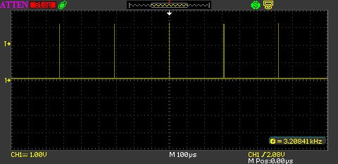
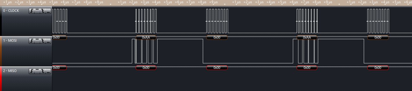
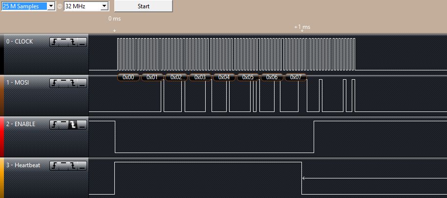
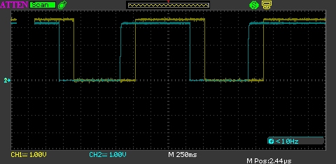
Compiling the above code and deploying it to the STM32 Discovery board generated the following output on the logic analyser:
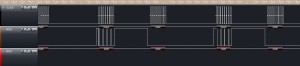
Polled SPI
A low clock speed is chosen for the SPI bus as it helps to eliminate the impact of interference from stay signals, long leads etc. Once the system is working at a low clock speed, the prescalar can be changed and the speed increased gradually until we determine the maximum rate at which data can be transmitted reliably.
The main program loop above contains two calls to the SPISend method. The first transmits the data we want top send to the slave device, the second call sends dummy data. This would allow the slave module to send a single byte response.
Interrupt Driven SPI
The final aim of this project is to be able to send data to an LED Panel using SPI. The panel itself is not required to send data back to the application. The modifications made here will take that into consideration. The following changes will be made:
- Transmit only, no data will be received
- Interrupt driven
- Heartbeat will kick off the transmission of the data
- Transmit a buffer of data (more than a single byte)
The first modification to be made is to the SPI configuration. Change the SPI_InitStruct setup to use a single Tx line and add code to configure the SPI interrupt priority:
SPI_InitStruct.SPI_Direction = SPI_Direction_1Line_Tx;
SPI_InitStruct.SPI_Mode = SPI_Mode_Master;
SPI_InitStruct.SPI_DataSize = SPI_DataSize_8b;
SPI_InitStruct.SPI_CPOL = SPI_CPOL_Low;
SPI_InitStruct.SPI_CPHA = SPI_CPHA_1Edge;
SPI_InitStruct.SPI_NSS = SPI_NSS_Soft | SPI_NSSInternalSoft_Set;
SPI_InitStruct.SPI_BaudRatePrescaler = SPI_BaudRatePrescaler_256;
SPI_InitStruct.SPI_FirstBit = SPI_FirstBit_MSB;
SPI_Init(SPI1, &SPI_InitStruct);
//
//    Configure the SPI interrupt priority
//
NVIC_PriorityGroupConfig(NVIC_PriorityGroup_2);
NVIC_InitStructure.NVIC_IRQChannel = SPI1_IRQn;
NVIC_InitStructure.NVIC_IRQChannelPreemptionPriority = 0;
NVIC_InitStructure.NVIC_IRQChannelSubPriority = 1;
NVIC_InitStructure.NVIC_IRQChannelCmd = ENABLE;
NVIC_Init(&NVIC_InitStructure);
This application will be sending a buffer of data rather than a repeated byte so we need to add somewhere to store the data. Adding the following to the SPI.c file gives us some storage:
//
//    Storage for the SPI data.
//
uint8_t buffer[SPI_BUFFER_LENGTH];
int bufferIndex = 0;
And adding the following to the SPI.h header file allows the storage to be accessible from other modules:
//
//    SPI related constants.
//
#define SPI_BUFFER_LENGTH        10

//
//    Data storage for the SPI methods.
//
uint8_t buffer[SPI_BUFFER_LENGTH];
int bufferIndex;
Ensure that the code is within the
extern “C” statement.
The final bit of the puzzle is the addition of the interrupt capability. The method chosen is to configure the SPI bus and leave SPI turned on but initially have the SPI interrupts turned off. The SysTick_Handler will act as the trigger for the SPI communication starting the communication by setting up the initial conditions and turning on the SPI interrupt. The SPI interrupt handler will take over from there. Modifying the SysTick_Handler we get:
//
//    System tick handler.
//
void SysTick_Handler(void)
{
    //
    //    Generate a heartbeat.
    //
    GPIOE->ODR ^= GPIO_Pin_5;
    //
    //    If we are about to generate a rising edge on the heartbeat
    //    we are ready to start SPI data transmission.
    //
    if (GPIOE->ODR & GPIO_Pin_5)
    {
        GPIOE->BSRRH |= GPIO_Pin_6;
        bufferIndex = 0;
        SPI_I2S_ITConfig(SPI1, SPI_I2S_IT_TXE, ENABLE);
    }
}
This code starts the SPI transmission on the rising edge of the heartbeat pulse. Note also that this interrupt handler is responsible for setting the chip select line.
The final bit of the puzzle is the SPI interrupt handler itself.
//
//    Process the interrupts for SPI1.
//
void SPI1_IRQHandler()
{
    //
    //    If TX buffer is empty then transmit the next byte.
    //
    if (SPI1->SR & SPI_I2S_FLAG_TXE)
    {
        if (bufferIndex < SPI_BUFFER_LENGTH)
        {
            SPI1->DR = buffer[bufferIndex++];
        }
    }
    //
    //    If SPI is not busy then we have finished sending data
    //    so turn off this interrupt.
    //
    if (!(SPI1->SR & SPI_I2S_FLAG_BSY))
    {
        SPI_I2S_ITConfig(SPI1, SPI_I2S_IT_TXE, DISABLE);
        GPIOE->BSRRL |= GPIO_Pin_6;
    }
    //
    //    Clear the interrupt pending bit otherwise this interrupt
    //    will be regenerated.
    //
    SPI_I2S_ClearITPendingBit(SPI1, SPI_I2S_IT_TXE);
}
Two key points to notice in this interrupt handler when the end of data buffer has been reached and SPI is no longer busy:
- Chip select is set to high
- Interrupts are disabled
The last line of this interrupt handler clears the SPI interrupt pending bit to prevent this handler being called again as soon as it exits.
One final modification to be made is to the main program loop. This is no longer required to control the transmission of the data but we will need to setup the contents of the data buffer:
//
//    Main program loop.
//
int main()
{
    Initialise();
    //
    //    Fill the SPI buffer with data.
    //
    int index;
    for (index = 0; index < SPI_BUFFER_LENGTH; index++)
    {
        buffer[index] = index;
    }
    //
    //    Main program loop.
    //
    while (1);
}
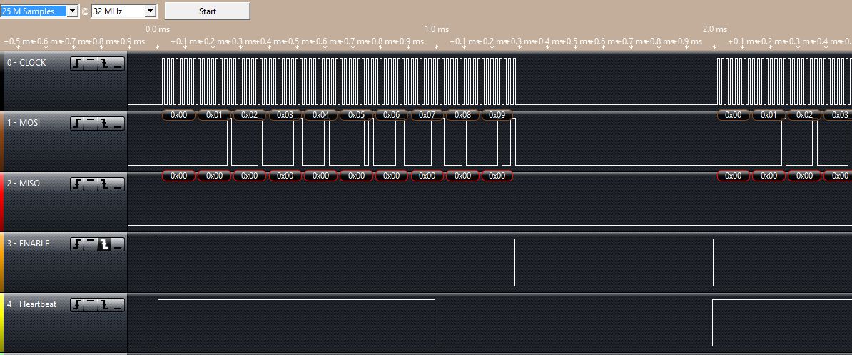
Putting all this together, compiling, deploying gives the following output on the logic analyser:
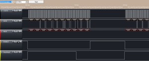
Buffered SPI With Heartbeat
SPI and DMA
The transition from polled SPI to interrupt driven SPI has so far reduced the load on the microcontroller but the STM32 has one final trick we can use, DMA (Direct Memory Access). DMA allows the various peripherals (of which SPI is one) to directly access the memory used for data storage/retrieval. By doing this the peripheral can operate autonomously until it has run out of data to process.
Remember the following in the SPI interrupt handler above:
if (bufferIndex < SPI_BUFFER_LENGTH)
{
    SPI1->DR = buffer[bufferIndex++];
}
This is required as the SPI peripheral generates an interrupt each time it has transmitted a byte of data and the buffer is empty. With DMA we can hand the SPI peripheral a block of data and tell it to transmit all of the data and simply tell us when the transmission has completed. This means we only receive one interrupt at the end of transmission rather than the 10 we receive for the above scenario.
First thing to do is to modify the InitialiseSPI method to configure the SPI peripheral to use DMA:
//
//    Initialise SPI
//
void InitialiseSPI()
{
    SPI_InitTypeDef SPI_InitStruct;
    NVIC_InitTypeDef NVIC_InitStructure;
    DMA_InitTypeDef DMA_InitStructure;
    //
    //     Connect SPI1 pins to SPI alternate function.
    //
    GPIO_PinAFConfig(GPIOA, GPIO_PinSource5, GPIO_AF_SPI1);
    GPIO_PinAFConfig(GPIOA, GPIO_PinSource6, GPIO_AF_SPI1);
    GPIO_PinAFConfig(GPIOA, GPIO_PinSource7, GPIO_AF_SPI1);
    //
    //    Set PE6 high as we will be using active low for the
    //    device select.
    //
    GPIOE->BSRRL |= GPIO_Pin_6;
    //
    //     Enable the SPI peripheral clock.
    //
    RCC_APB2PeriphClockCmd(RCC_APB2Periph_SPI1, ENABLE);
    //
    //    Configure SPI1 in Mode 0:
    //        CPOL = 0 --> clock is low when idle
    //        CPHA = 0 --> data is sampled at the first edge
    //
    //    SPI Master mode, 8 bits of data, clock prescalar is 128, MSB is
    //    transmitted first.
    //
    SPI_InitStruct.SPI_Direction = SPI_Direction_1Line_Tx;// SPI_Direction_2Lines_FullDuplex;
    SPI_InitStruct.SPI_Mode = SPI_Mode_Master;
    SPI_InitStruct.SPI_DataSize = SPI_DataSize_8b;
    SPI_InitStruct.SPI_CPOL = SPI_CPOL_Low;
    SPI_InitStruct.SPI_CPHA = SPI_CPHA_1Edge;
    SPI_InitStruct.SPI_NSS = SPI_NSS_Soft | SPI_NSSInternalSoft_Set;
    SPI_InitStruct.SPI_BaudRatePrescaler = SPI_BaudRatePrescaler_256;
    SPI_InitStruct.SPI_FirstBit = SPI_FirstBit_MSB;
    SPI_Init(SPI1, &SPI_InitStruct);
    //
    //    Configure the DMA controller
    //
    RCC_AHB1PeriphClockCmd(RCC_AHB1Periph_DMA2, ENABLE);
    DMA_StructInit(&DMA_InitStructure);
    DMA_InitStructure.DMA_Channel = DMA_Channel_3;
    DMA_InitStructure.DMA_PeripheralBaseAddr  = (uint32_t) &(SPI1->DR);
    DMA_InitStructure.DMA_Memory0BaseAddr  = (uint32_t) &buffer;
    DMA_InitStructure.DMA_DIR = DMA_DIR_MemoryToPeripheral;
    DMA_InitStructure.DMA_BufferSize  = SPI_BUFFER_LENGTH;
    DMA_InitStructure.DMA_PeripheralInc  = DMA_PeripheralInc_Disable;
    DMA_InitStructure.DMA_MemoryInc  = DMA_MemoryInc_Enable;
    DMA_InitStructure.DMA_PeripheralDataSize  = DMA_PeripheralDataSize_Byte;
    DMA_InitStructure.DMA_MemoryDataSize  = DMA_MemoryDataSize_Byte;
    DMA_InitStructure.DMA_Mode  = DMA_Mode_Normal;
    DMA_InitStructure.DMA_Priority  = DMA_Priority_High;
    DMA_InitStructure.DMA_FIFOMode  = DMA_FIFOMode_Disable;
    DMA_Init(DMA2_Stream5, &DMA_InitStructure);
    DMA_ITConfig(DMA2_Stream5, DMA_IT_TC, ENABLE);

    NVIC_InitStructure.NVIC_IRQChannel = DMA2_Stream5_IRQn;
    NVIC_InitStructure.NVIC_IRQChannelPreemptionPriority = 0;
    NVIC_InitStructure.NVIC_IRQChannelSubPriority = 1;
    NVIC_InitStructure.NVIC_IRQChannelCmd = ENABLE;
    NVIC_Init(&NVIC_InitStructure);
    //
    //    Enable SPI.
    //
    SPI_Cmd(SPI1, ENABLE);
}
The DMA controller is configured for memory to peripheral data transfer (from the buffer to the SPI->DR register). The pointer into memory is incremented after each transmission but the destination pointer (SPI->DR) remains fixed. The system will use DMA2, channel 3, stream 5. The choice of the DMA peripheral, stream and channel has some freedom but is constrained by the choice of peripheral. The list of allowed choices can be found in the STM32 Programmers Reference. As we are using SPI1 we are forced to use DMA2, channel 3 but we can choose between streams 3 and 5.
The next thing to do is to add a new interrupt handler for the DMA completion interrupt:
//
//    SPI DMA handler.
//
void DMA2_Stream5_IRQHandler()
{
    //
    //     Test if DMA Stream Transfer Complete interrupt
    //
    if (DMA_GetITStatus(DMA2_Stream5, DMA_IT_TCIF5) == SET)
    {
        DMA_ClearITPendingBit(DMA2_Stream5, DMA_IT_TCIF5);
        //
        //    The following is required to ensure that the chip select is not
        //    changed while data is still being transmitted.
        //
        while (SPI_I2S_GetFlagStatus(SPI1, SPI_I2S_FLAG_BSY) == SET);
        //
        //    Now set chip select to high.
        //
        GPIOE->BSRRL |= GPIO_Pin_6;
    }
}
Make a note of the while loop in the middle of the if statement. We will come back to this later.
The final piece of work is to modify the SysTick_Handler method:
//
//    System tick handler.
//
void SysTick_Handler(void)
{
    //
    //    Generate a heartbeat.
    //
    GPIOE->ODR ^= GPIO_Pin_5;
    //
    //    If we are about to generate a rising edge on the heartbeat
    //    we are ready to start SPI data transmission.
    //
    if (GPIOE->ODR & GPIO_Pin_5)
    {
        GPIOE->BSRRH |= GPIO_Pin_6;
        DMA2_Stream5->M0AR = (uint32_t) &buffer;
        DMA_Cmd(DMA2_Stream5, ENABLE);
        SPI_I2S_DMACmd(SPI1, SPI_I2S_DMAReq_Tx, ENABLE);
    }
}
As with the previous interrupt example, this method starts the transfer process.
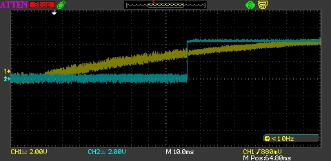
Putting this together in a project, compiling and deploying gives the following output on the logic analyser:

Multiple DMA SPI Transfers
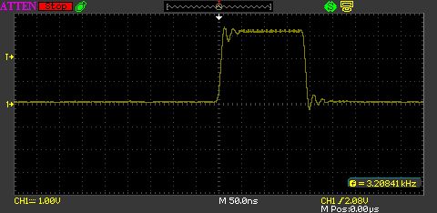
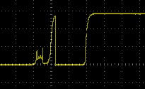
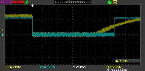
Remember the while loop above. This is necessary as the DMA transfer complete interrupt is generated as soon as the data has been transferred from memory to the SPI peripheral. This does not necessarily mean that the data has been transferred to the slave device connected to the SPI bus. If we did not have the loop in the handler to check that the transfer had completed we could end up in a situation where the chip select line to taken high before data transfer has completed. This is verified by the following trace on the logic analyser:

Enable Asserting Before Transfer Complete
Note how chip select goes high when we still have nearly a full byte of data to transmit.
Conclusion
What started out as an investigation into the control of an LED panel turned into a marathon investigation into SPI on the STM32. This post has presented three different methods for controlling data transfer over SPI each having its own merits. The source code for the CooCox projects can be downloaded here:
- Polled SPI
- Interrupt driven SPI
- SPI and DMA