RSS

Archive for the ‘Software Development’ Category

STM8S SPI

Wednesday, May 16th, 2012

In this latest in the series I am taking a look at communication between two systems (namely a Netduino Mini and a STM8S103) using SPI.

As with previous articles the system will use the IAR compiler and the STD Peripheral Library. The Netduino Mini will use Visual Studio and .NET to act as the master for the SPI bus.

I ran into some problems along the way and had to ask for help in the Netduino Forums. Special mention to Chris Walker and CW2 for their help.

Netduino Mini Application

SPI is one of the protocols supported by the NETMF framework on the Netduino platform. As such there is little work to do. The Mini will have to act as the SPI master as this is the only role which is supported on the Netduino for this bus. We simply need to set up the SPI bus with the correct parameters and then start writing data to the bus.

To remove as many possible problems as possible we will perform a simple task, have the Netduino Mini write some data to the bus on a regular basis. In this case we will write three bytes with the values 1, 2 and 3. The code on the Mini is as simple as the following:

public static void Main()
{
	SPI.Configuration config = new SPI.Configuration(SPI_mod: SPI.SPI_module.SPI1,
							   ChipSelect_Port: Pins.GPIO_PIN_5,                        // Enable pin is D5.
							   ChipSelect_ActiveState: false,                           // Active Low
							   ChipSelect_SetupTime: 0,                                 // 0 uS setup time.
							   ChipSelect_HoldTime: 0,                                  // 0 uS hold after data transmission has completed.
							   Clock_IdleState: false,                                  // Clock line is low when the device is inactive.
							   Clock_Edge: false,                                       // Data is sampled on the clock falling edge.
							   Clock_RateKHz: 500);                                     // 500 KHz clock speed.

	SPI spi = new SPI(config);

	byte[] buffer = new byte[] { 1, 2, 3 };
	while (true)
	{
		spi.Write(buffer);
		Thread.Sleep(1000);
	}
}

This code configures the bus as follows:

  • Chip select will be D5 on the Netduino Mini
  • Chip select will be active low
  • Clock is low when the device is inactive
  • Data is sampled on the falling edge of the clock signal
  • Clock rate is 500 KHz

The selection of these values is deliberate as they match the values used on the GO! bus.

STM8S Code

This is where it got tricky and where I need some help. We have a simple application on the Netduino Mini which simply sends out three bytes, waits a second and then repeats. In order to know that we have received this data OK, the application on the STM8S will read these bytes from the SPI bus, add 100 and then send the result back to the Mini.

The first thing we need to do is to set up a project similar to the first article in this series. The main STD Peripheral Library module we will be using here is the SPI library which can be found in stm8s_spi.c. Add this to the project and then reference the stm8s_spi.h in the main program file.

Now we have the SPI library referenced and the library file added to the application we need to start using it. So the first step we need to take is to configure the library ready for use. The following code should achieve this matching the parameters we have set up in Netduino Mini project above.

SPI_DeInit();
SPI_Init(SPI_FIRSTBIT_MSB,                      // MSB first.
		 SPI_BAUDRATEPRESCALER_32,              // For slave comms this does not matter as the clock is controlled by the master.
		 SPI_MODE_SLAVE,                        // SPI Slave
		 SPI_CLOCKPOLARITY_LOW,                 // Clock is high when the bus is idle.
		 SPI_CLOCKPHASE_2EDGE,                  // Falling clock edge clocks the first data bit.
		 SPI_DATADIRECTION_2LINES_FULLDUPLEX,   // Full duplex transmission.
		 SPI_NSS_HARD,                          // Disable slave management by software.
		 0x07);                                 // CRC style.
SPI_ITConfig(SPI_IT_RXNE, ENABLE);              // Interrupt when the Rx buffer is not empty.
SPI_ITConfig(SPI_IT_TXE, ENABLE);               // Interrupt when the Tx buffer is empty.

The first this we do is call SPI_DeInit to reset any SPI bus configuration.

Next we call SPI_Init to configure the system, as a SPI slave using the same parameters as the SPI master (i.e. the Netduino Mini). You should not that although the baud rate prescalar parameter is set here it will be ignored. The master controls the clock on the SPI bus.

The final two statements (SPI_ITConfig statements) determine which actions will generate an interrupt. In this case we are instructing the system to generate an interrupt in the following cases:

  • When the Rx buffer is not empty (i.e. data has been received)
  • When the Tx buffer is empty (i.e. the system is ready to send more data)

Interrupt Handler

The data will be handled by an interrupt handler. This handler will be called when we need to send data or when we have data ready for processing. As before, the handlers can be found in the file stm8s_it.c. The handler we will be looking for is the SPI_IRQHandler. Locate this handler and replace the code with the following:

INTERRUPT_HANDLER(SPI_IRQHandler, 10)
{
    if (SPI->SR & SPI_SR_RXNE)
    {
        //  u8 ch = SPI_ReceiveData();
        u8 ch = SPI->DR;
        //  SPI_SendData(ch + 100);
        SPI->DR = ch + 100;
    }
    SPI->SR = (u8) 0;
}

The two lines commented out are the equivalent calls into the SPI library. Remember that ISR’s should be as fast as possible. Replacing the calls with the appropriate expansions will decrease the amount of time required to execute the ISR.

So, here we check to see if the ISR is being called because the Rx buffer is not empty. If the buffer is not empty then we extract the value from the buffer, add 100 to it and then put this in the Tx buffer.

The final thing we do is to clear the interrupt from the status register.

Main Program Loop

The code in the main program queues up a byte ready for transmission, enables the interrupts and then repeatedly waits for more interrupts. The code looks like this:

int main(void)
{
    Initialise();
    SPI_SendData('*');                          // Ready to send before master can initiate transfer.
    enableInterrupts();                         // Make sure interrupts are enabled.
    while (1)
    {
        wfi();
    }
}

So What Happened?

After spending a fair amount of time with the logic analyser and the debugger I hit a brick wall. The interrupts we not getting fired as I expected. This is where Chris Walker and CW2’s help was required. The point I was missing regarded the SPI_NSS signal. On the STM8S103 chip I was using this function is an alternative function for the labelled pin. In order to allow this pin to act as the chip select for the SPI bus it was necessary to set the alternative function register on the chip. Once this was set correctly the system started to generate interrupts as expected.

STM8S Interrupts With the STD Peripheral Library

Saturday, May 12th, 2012

So you have just purchased that wonderful sensor and now need it to grab the attention of the STM8S – enter the interrupt. In this post I will run through how to set up a GPIO port to have an incoming logic signal generate an interrupt.

As in previous posts on the STM8S, this post will use the IAR development environment and the STD Peripheral Library from ST.

Configuring the Port

The first step is to configure a port for input. The following code configures a pin on GPIOB for input:


GPIO_DeInit(GPIOB);
GPIO_Init(GPIOB, GPIO_PIN_5, GPIO_MODE_IN_FL_IT);

the next thing we need to do is to tell the system that this pin is allowed to generate an interrupt:


EXTI_SetExtIntSensitivity(GPIOB, 
                          EXTI_SENSITIVITY_RISE_ONLY);

So that should be all that’s required to configure the system to accept interrupts. Now we just need to process them.

Interrupt Handler

If you have followed my previous posts you will know that we need to copy some standard files across in order to access the STD Peripheral Library. One of the files we add to the project is stm8s_it.c. This holds the interrupt table for the chip. Scroll through the file and you will eventually reach some code which looks like this:


INTERRUPT_HANDLER(EXTI_PORTB_IRQHandler, 4)
{
  /* In order to detect unexpected events during development,
     it is recommended to set a breakpoint on the following instruction.
  */
}

Just place the code to be executed in this method. Remember, interrupt handlers should be small and concise.

Modules

This post requires that you add the code files for the following STD Peripheral Library modules:

  • stm8s_gpio.c
  • stm8s_exti.c

Conclusion

A relatively short post but there’s not much too it. I have successfully used this code to generate an interrupt from a sensor which generates a square wave of up to 500 KHz. The conditions I was using it in gave a maximum frequency of 20 KHz.

STM8S Timers

Saturday, May 12th, 2012

This post has been superseded by the post Using Timers on the STM8S in The Way of the Register series.

In the first post about this chip I showed how the internal clock could be output on a single pin. Here I am going to use one of the internal timers to generate my own clock signal. So in this post we will use two new concepts:

  • GPIO pins to output a signal.
  • Timer 2 to control the timing
  • Interrupt Service Routines (ISR) to do the work

The program will work by setting up timer 2 to generate an interrupt on a regular basis. When the timer interrupt fires we will reverse the direction of a GPIO pin. The net result will be a clock signal with a frequency of twice that of the timer.

As with the previous post I will be using the IAR environment with the STD Peripheral Library.

Setting up the GPIO

The application sets up the GPIO port using the following code:

#define CLOCK_OUTPUT_PORT       GPIOD
#define CLOCK_OUTPUT_PIN        GPIO_PIN_3

These #defines hold the port and pin numbers we are going to use for the clock signal. So in this case we are using pin 3 on port D. Next we need to configure the port.

GPIO_DeInit(CLOCK_OUTPUT_PORT);
GPIO_Init(CLOCK_OUTPUT_PORT, CLOCK_OUTPUT_PIN, GPIO_MODE_OUT_PP_LOW_FAST);

The first statement resets the port so that we can configure the port. The second sets up pin 3 of port D for use. Note that you can use each pin on a port in a different way, so we could have pin 2 on port D as an input whilst pin 3 is an output. To do this you simply add more GPIO_Init statements under the first. Now let’s have a look at the final parameter to the GPIO_Init statement. This defines how the pin will be set up for us. You can decode this as follows:

  • GPIO_MODE_OUT – this is an output port
  • PP – the pin will be used in Push-Pull (as opposed to open drain). This means Setting the pin to 1 will make the pin high, setting it to 0 will make it low.
  • LOW – the pin will start out low
  • FAST – the pin will be used for fast signalling.

Setting up Timer 2

Next step is to configure the timer to interrupt on a regular basis. The first step is to set up the clock to use a known clock signal. For simplicity we will set this up to use the internal high speed clock source which runs at 16MHz. This code is similar to the code in the first post.

CLK_DeInit();
CLK_SYSCLKConfig(CLK_PRESCALER_CPUDIV1);                // CPU Prescaler = 1.
CLK_SYSCLKConfig(CLK_PRESCALER_HSIDIV1);                // Prescaler = 1, 16 MHz.
CLK_ClockSwitchConfig(CLK_SWITCHMODE_AUTO,              // Automatically switch
                      CLK_SOURCE_HSI,                   // Switch to internal timer.
                      DISABLE,                          // Disable the clock switch interrupt.
                      CLK_CURRENTCLOCKSTATE_DISABLE);   // Disable the previous clock.

The only real difference is that the prescaler for the system clock is set to 1 to give the full clock speed.

The next task is to set up the timer to run at a particular frequency:

TIM2_DeInit();
TIM2_TimeBaseInit(TIM2_PRESCALER_4096,      // Interrupt every 4096 clock pulses.
                  1);                       // Period is one.
TIM2_ITConfig(TIM2_IT_UPDATE, ENABLE);      // Enable the overflow interrupt.
TIM2_Cmd(ENABLE);

The comment interrupt every half millisecond is approximate as you will see when we come to take some measurements later.

The Interrupt Service Routine

The final piece of the puzzle is the interrupt service routine. These should always be small and fast. In this case we will simply toggle the specified clock pin to generate a clock signal.

All of the ISR’s are defined in the file stm8s_it.c. The ISR we will be working with is the timer 2 update overflow handler. This will fire when the counter for the timer overflows or becomes zero and the specified number of occurrences of this event have occurred. So in this file we need to locate this code:

INTERRUPT_HANDLER(TIM2_UPD_OVF_BRK_IRQHandler, 13)
{
}

and translate it to this:

INTERRUPT_HANDLER(TIM2_UPD_OVF_BRK_IRQHandler, 13)
{
    GPIO_WriteReverse(CLOCK_OUTPUT_PORT, CLOCK_OUTPUT_PIN);     // Generate a clock signal.
    TIM2->SR1 = (uint8_t) (~(uint8_t) TIM2_IT_UPDATE);          // Clear the interrupt.
}

The first line of the ISR toggles the specified bit. The second line is important as this clears the interrupt. If we do not do this then the system will return to this ISR as soon as we exit the routine.

Clock Signal

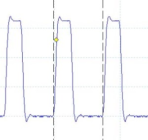
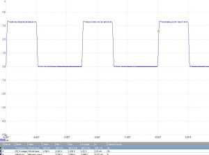
Compiling and deploying this code to the processor results in the following output on pin 3 of port D:

One millisecond clock signal on port D, pin 3.

The scope we set up for 2 milliseconds per division and this looks about right. The exact frequency count comes out to be 976.6 Hz which is right if you divide the clock signal by the prescaler.

Netduino Go! Module Development – the First Steps

Friday, April 27th, 2012

The last few weeks I’ve been getting things together to start to look at developing a smart module for the Netduino GO!. This post looks at the first steps and ends up with some working code on a STM8S003 chip.

STM8S Discovery

My starting point was to get the software tools installed and working. In order to verify this I purchased the STM8S Discovery board. This has the STLink module and a STM8S105 microcontroller built into a convenient package for less than £7.00. This board itself was easy to set up and worked straight out of the box.

Development Environment

Having the board is one thing but we need a development environment to work with. I tried several environments and in the end I found I was happiest with the IAR environment so for the moment I’m sticking with it whilst I find my feet. Set up was easy and it found the STM8S Discovery straight away.

Start With Something Simple

I wanted to start with a really simple project which would not require any additional hardware other than a scope to check that the application was working. That way I could transfer the program to a microcontroller on a breadboard and know that I had as few possible points of failure as possible. To this end I decided that I would put the microcontroller clock pulses out on one of the pins. I could verify that everything was working but uploading a new program which changed the clock scaler and if all was well I would see a different trace on the scope.

This choice of application was no accident as the data sheet for the chip shows that it has a pin labelled CCO. You can configure this pin to output the controller’s clock signal. Not only that but you can also use the microcontroller’s internal clock generator as the clock signal. So in theory, all I needed to do was add a few discrete components to the breadboard along with the STM8S and I should have a small, simple, self contained system to test the tool set.

Creating a New Project

First thing to do is create a new workspace and project using IAR. Simple enough, enter a name for both and a new main.c is presented to you. Good game but not much use as it stands.

Luckily ST provide a standard library of drivers for the various features available on their chip sets. I downloaded version 2.1.0 of the library and this contained the drivers and some sample applications. The trick is to understand the way in which you access the libraries. It’s really simple and basic. In effect, you add the C source files for the library to your application and compile your application and the libraries at the same time. Both of these are then deployed as a single binary to the microcontroller. Basic but it works. The source files are broken down by microcontroller feature. So, all of the routines etc. for timer 2 are in the header file stm8s_tim2.h and the source code is in the file stm8s_tim2.c.

To make things easier (well, easier for me anyway) I have taken to copying the source and include files from the standard library provided into each project directory I create. That way you simply need to add the source file for a feature as you need it. In this case the only feature I’m going to be using is the clock and so I need to make sure I add the stm8s_clk.c file to the project.

The stm8s.h file contains definitions for a whole range of controllers. It is therefore necessary to define a preprocessor macro for the type of controller the application is targeting. This can be done in one of two ways, either in the stm8s.h file itself (as this in included in the other standard library files) or as a macro in the project. I personally prefer to do this in the project as it makes updating the library code easier.

So Let’s Get Started

First thing to do is to get a workspace and project created. So open IAR and create a new workspace. Next, go to the Project Menu and create a new project. The following dialog should appear:

New Project Dialog

Select a C project and click OK. The next dialog asks you to select a name and location for the project. So decide on a location and name. Being very creative, I went for Test as the project name. Once completed I had a project which looked like this:

New C Project.

The next job is to add the include and source files for the standard peripheral library. So copy the include and source files from the library and add them to the directory containing your project. I normally put the include files in the inc directory and the sources in the src directory. The next thing to do is add these files to the project. So right click on the project name (in this case Test – Debug and select Add – Add Group. Enter the name STD Peripheral Include

Add new file group

Repeat this to add the source file group with the name STD Peripheral Source. Your project should now look like this:

File Groups Added to Project

Now we need to add the files to the groups. For the include files I add all of the files. For the source files I only add the ones I will be using. To do this you right click on one of the file groups we have created, say the STD Peripheral Include group and select Add – Add Files…. For the include files navigate to the directory containing the copied files and select them all.

Repeat for the source files but this time we only select the files we will be using. In this case the clock file stm8s_clk.c. Your project should now look something like this:

All Files added

There are still a few extra steps before we can write some code. The STM8S include files require that the type of chip is defined before any code will compile so we will need to define a preprocessor macro indicating which chip we are using. Next we need to tell the compiler about the location of the include files. Finally, we need to tell the system how to deploy and debug the application.

So let’s start off with the chip family. Firstly we want to tell the compiler about the target family. So right click on the project name and this time select Options. Under General options, select the chip family to be targeted. For the Discovery board the family is STM8S105, for the final module we will be targeting the STM8S003.

Select chip family.

The next step is to tell the preprocessor about the chip family and the location of the include files. From the same dialog as above, select the C/C++ compiler and the Preprocessor tab. Add the entry $PROJ_DIR$inc to the include files and define a symbol for the chip set. Define STM8S105 for the Discovery board and STM8S003 for the final module.

Pre-processor Options

The final step is to tell the IDE how to deploy and debug the application. From the Options dialog select the Debugger category and set the Driver to ST-LINK.

Debugger Options.

Now click on OK to set the options. We can now start to write some code.

Let’s Write Some Code

Replace the code in the main.c file with the following:

#include "stm8s.h"
#include "stm8s_clk.h"

int main(void)
{
    CLK_DeInit();
    CLK_SYSCLKConfig(CLK_PRESCALER_CPUDIV1);                // CPU Prescaler = 1.
    CLK_SYSCLKConfig(CLK_PRESCALER_HSIDIV8);                // Prescaler = 8, 2 MHz.
    CLK_CCOConfig(CLK_OUTPUT_HSI);                          // Output clock on CCO pin.
    CLK_ClockSwitchConfig(CLK_SWITCHMODE_AUTO,              // Automatically switch
                          CLK_SOURCE_HSE,                   // Switch to internal timer.
                          DISABLE,                          // Disable the clock switch interrupt.
                          CLK_CURRENTCLOCKSTATE_DISABLE);   // Disable the previous clock.
}

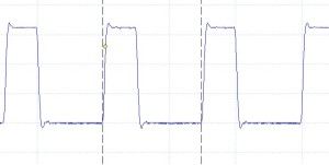
Connect up board/chip and hit Ctrl-D. This will compile and deploy the application. The debugger should start with the first line of main highlighted. Press F5 and the application should start. Hooking up the oscilloscope gave the following trace:

Oscilloscope Output

The clock frequency of the chip using the internal high speed oscillator is 16 MHz. Diving this by 8 should give a 2 MHz signal (as indeed the above trace shows). Just to check if this is a coincidence, change to CLK_PRESCALER_HSIDIV8 to say CLK_PRESCALER_HSIDIV4 and the scope output should change to show the new clock frequency and sure enough it does.

STM32F4 Discovery – First Impressions

Monday, March 19th, 2012

I recently came across the STM32F4 Discovery board. This board is an ARM processor on a board with 1MB flash and 192KB RAM, ADC, Audio processing, motion detection USB for both debugging and HID support – not bad for less than £10. Given the price and a bit of research and I thought I’d risk it.

So the board arrived and now it’s time to set up the tool chain. There are several toolchains available but the one which was attractive was the Atollic toolchain. The LITE version 2.3 IDE had no code limitations and instead it limited the features available through the IDE. Note that since buying the board and downloading the software Atollic have gone down the route of removing the restrictions on the IDE and placing a code size restriction on the environment. This fits in with the approach taken by several of their competitors.

Installing the Software and the Board

Installation of the software and the board seemed to go OK. Connecting the board found a few problems. The first problem came from the samples. I imported the directory containing the samples and this seemed to pull in the samples for the Atollic system and also the samples for other development environments. This resulted in multiple projects with the same name and this (understandably) upset the Atollic environment. So a quick play with explorer deleting the extra projects and the remaining projects imported with now issues.

The second project came when I tried to compile, deploy and debug one of the samples. The debugger kept complaining that it could not find the board. Hello Google. The problem was simple to solve and all it required was to reinstall the driver for the board. All this required was to open control panel, selecting the board and then update the driver.

So far, so good. I have the board installed along with the software and I can deploy the sample projects.

Can I write my own software?

My First Application

For my first application I wanted to do a bit more than just flash the onboard LEDs, not much more but I wanted some indication of the speed of the board. So I decided to simply toggle one of the ports and look at this through a logic analyser.

So the first thing to do is to create a new project. So off to the file menu and I selected new project. The restricted version of the development environment does not allow C++ projects so I went for a C project and selected Embedded C Project:

Next I selected the board and hardware settings for the build:

And the final step is to configure the debugger settings:

Next thing to do was to modify the default sample code. I opened the main.c file and replaced the main program loop with the following:

GPIO_InitTypeDef  GPIO_InitStructure;

STM_EVAL_LEDInit(LED3);
STM_EVAL_LEDInit(LED4);
STM_EVAL_LEDInit(LED5);
STM_EVAL_LEDInit(LED6);

/* Turn on LEDs */
STM_EVAL_LEDOn(LED3);
STM_EVAL_LEDOn(LED4);
STM_EVAL_LEDOn(LED5);
STM_EVAL_LEDOn(LED6);

int flag = 0;
GPIO_InitStructure.GPIO_Pin = GPIO_Pin_0;
GPIO_InitStructure.GPIO_Mode = GPIO_Mode_OUT;
GPIO_InitStructure.GPIO_OType = GPIO_OType_PP;
GPIO_InitStructure.GPIO_Speed = GPIO_Speed_100MHz;
GPIO_InitStructure.GPIO_PuPd = GPIO_PuPd_NOPULL;
GPIO_Init(GPIOD, &GPIO_InitStructure);
while (1)
{
    if (flag)
    {
        GPIO_SetBits(GPIOD, GPIO_Pin_0);
        flag = 0;
    }
    else
    {
        GPIO_ResetBits(GPIOD, GPIO_Pin_0);
        flag = 1;
    }
}

Hooking up the logic analyser to Port D, pin 0 gave a square wave with a frequency of about 2.25 MHz.

Success!

Back to the samples and lets see where it takes us.

Silverlight 5 Released

Saturday, December 10th, 2011

Just read that Silverlight 5 has just been released. Off to the downloads page and some replanning of this weekends activities.

For more information visit the Silverlight home page.

Cascading TLC5940 LED Drivers

Wednesday, November 2nd, 2011

A while ago I created a circuit and some code to control the TLC5940 LED driver using a Netduino Mini. This chip allowed the programmer to control 16 LEDs using a serial interface. In the conclusions I noted that it should be possible to control two or more of these chips by cascading the serial output from one chip into another. This article discusses the additional hardware required along with the software to control up to 32 LEDs using two of these chips linked together.

It is assumed that you have read and understood the previous article before you proceed further.

Hardware

Linking two of these chips is a relatively simple affair and requires the LEDs you wish to control and only 1 additional component, namely a 2K2 ohm resistor, and some additional wire (assuming you are using breadboard).

Starting with the simplest part, the 2K2 ohm resistor connects the IREF pin on the second TLC5940 to ground. This sets the reference voltage for the LEDs connected to the second TLC5940.

The next part of the problem is to connect the two chips together. This is achieved by connecting the following pins:

TLC5940 (1)TLC5940 (2)
SCLKSCLK
BLANKBLANK
XLATXLAT
GSCLKGSCLK
VPRGVPRG
SOUTSIN
XERRXERR

DCPRG on TLC5940 is connected to Vcc as it is on the first driver chip and the LED controller pins connected to the appropriate LEDs.

This PDF (PWMLEDControlv0.03.pdf) contains the full circuit diagram showing the connections required.

Software

Now we have the additional LEDs in the circuit we will need to be able tell the software driver for the chips how many LEDs we want to control and then be able to control the brightness of the LEDs. In order to do this an additional parameter was added to the constructor numberOfLEDs. This parameter allows the system to work out how many TLC5940’s should be connected together. Once we have the number of chips calculated we can then work out the size of the buffers for the Dot Correction and the Grey Scale data.

The class uses two buffers for both the Dot Correction and the Grey Scale data. This may seem superfluous but doing this allows two different modes of operation:

  • Basic – The LEDs can be controlled using an interface which is simpler to use but is slower.
  • Fast – This mode is faster but requires the programmer to perform some of the tasks in the driver. The assumption here is that the programmer will have more understanding of the data which is changing and can therefore write more optimised code.

For the moment we will be discussing the basic mode. In this mode, the software driver hides much of the implementation and the user only really needs to perform three tasks:

  • Construct a new instance of the software driver.
  • Set the brightness of the LEDs (only the lower 12 bits are used).
  • Tell the driver to output the data to the TLC5940 chips.

Constructor

Making a new instance of the class in it’s most basic form is simply a case of telling the constructor how many LEDs you wish to control. In this case we have two TLC5940s connected together and so we have 32 LEDs:

Tlc5940 leds = new Tlc5940(numberOfLEDs: 32);

You can of course use the additional parameters to define the pins used for the various control signals or just use the defaults.

Setting a LED

The class contains a method which overloads the array indexing operator. Setting the brightness for a LED is simply a case of using this operator as follows:

leds[10] = 767;

This will set the brightness of LED 10 to the value 767.

An important note here is that the LEDs are numbered from 0 to 15 on the TLC5940 connected to the Netduino Mini, 16 to 31 on the next LED in sequence and so on.

Lighting the LEDs

The final piece of the puzzle is to output the data to the series of TLC5940s connected to the Netduino Mini. This is achieved by calling the Display method in the Tlc5940 class.

Source Code

The source code for the controller class and a simple main program can be found here (CascadedTLC5940.zip).

Conclusion

The work with this chip has not yet finished as there are still some points which need addressing in order to round off this class:

  • Dot Correction – this current outputs all 1’s and so there is no fine control for any of the outputs.
  • Error Detection and Status Information – It is possible to detect two types of errors and retrieve the status information from the TLC5940. This needs implementing.

One final item which needs addressing is to round off the code once these final feature have been implemented. A topic for another day.

So What’s All This About a Matrix?

Tuesday, July 5th, 2011

In a previous post I mentioned that replacing a single LED in the centre of a matric would be murder and so it will be. The matrix I have in mind is an 8 x 8 x 8 LED cube controlled by a Netduino board. Now it should be obvious that there are not enough pins to connect 512 LEDs to the Netduino without some magic being involved. This is where the Persistence of Vision post comes into the picture. In theory, it should be possible to control an array using a group of shift registers and a multiplexer circuit. So for the next few weeks this is what I’ll be looking at.

Multi-Threading

The previous post on Persistence of Vision had a simple while loop which allowed 16 LEDs to be controlled from the main program loop. In the final program this will be too cumbersome and timing is almost certainly to become an issue. To overcome this we will need to have the display logic separated from the control logic. This will allow the display to be continuously updated whilst the main program loop is working out what should be displayed next. The following tests this concept by turning on on LED at a time in a bank of 8. If this project has a chance of working then the 8 LEDs should all appear to be switched on permanently.

Hardware

The hardware is relatively simple. We have one shift register connected to the Netduino. This is in turn connected to 8 LEDs through current limiting resistors. The schematic looks something like this:

Persistence of Vision Threaded Display Driver Test Circuit

Software

The software requires us to take the display logic from previous posts and add this to a new class. This class will need to have a method executing in it’s own thread in order to allow the main program and the display driver to run at the same time. So splitting the display code into it’s own class we get something like this:

class LEDCube
{
    /// <summary>
    /// SPI bus to use to send data to the shift registers.
    /// </summary>
    SPI spi = null;

    /// <summary>
    /// CSPI bus configuration
    /// </summary>
    SPI.Configuration config;

    /// <summary>
    /// Buffer holding the display data.
    /// </summary>
    private byte[] buffer;

    /// <summary>
    /// Constructor for the LEDCube class.
    /// </summary>
    public LEDCube()
    {
        config = new SPI.Configuration(SPI_mod: SPI.SPI_module.SPI1,
                                       ChipSelect_Port: Pins.GPIO_PIN_D9,
                                       ChipSelect_ActiveState: false,
                                       ChipSelect_SetupTime: 0,
                                       ChipSelect_HoldTime: 0,
                                       Clock_IdleState: true,
                                       Clock_Edge: true,
                                       Clock_RateKHz: 400);

        spi = new SPI(config);
        buffer = new byte[1];
        buffer[0] = 0;
    }

    /// <summary>
    /// Main loop which continuously updates the display from the buffer.
    /// </summary>
    public void DisplayBuffer()
    {
        while (true)
        {
            lock (buffer)
            {
                spi.Write(buffer);
            }
        }
    }

    /// <summary>
    /// Change the byte in the display buffer.
    /// </summary>
    /// <param name="b">Byte to put into the buffer.</param>
    public void UpdateBuffer(byte b)
    {
        lock (buffer)
        {
            buffer[0] = b;
        }
    }
}

Much of the code should be familiar, we have the SPI bus and config variables along with a constructor to make a new instance of the SPI bus. The new code is really the DisplayBuffer and the UpdateBuffer methods.

  • DisplayBuffer is the method which has replaced the part of the main program loop which outputs the data to the SPI bus. This method is run in it’s own thread.
  • UpdateBuffer simply copies new data from the caller into the display buffer.

Note that both of these methods use locking to ensure that the methods are thread safe.

The main program loop now looks something like this:

LEDCube cube = new LEDCube();
Thread display = new Thread(new ThreadStart(cube.DisplayBuffer));
display.Start();
while (true)
{
    byte value = 1;
    for (int index = 0; index < 8; index++)
    {
        cube.UpdateBuffer(value);
        value <<= 1;
    }
}

A new LEDCube is created and at first this is not running in it’s own thread. The next two lines create and start a new thread. The thread is executing the DisplayBuffer method. We then start the main program lopp which simply sets each bit in a byte and the updates the buffer in the cube using UpdateBuffer.

Next step, build the control logic for 512 LEDs.

Persistence Of Vision

Saturday, June 11th, 2011

By chance last week end I came across a post discussing persistence of vision. This set me wondering if I could demonstrate this using the Netduino. First a little background.

Background

Persistence of vision is the phenomena which allows you to watch a movie. The projector shows a single still image on the screen. This is then replaced 1/24th of a second later by a new image. The projector achieves this by covering the image with a shutter whilst the frame is moved into place. We do not see the blank screen, just the previous frame. A fuller description can be found on this Wikipedia page.

We will be using this effect to control 27 LEDs using only 11 control lines. These lines will be the outputs from two 74595 shift registers which in turn will be connected to a Netduino Plus.

The Problem

The 27 LEDs will be split into three banks of 9. The aim will be to write a small program which will turn on one or more of the of the 9 LEDs in each bank in turn. If we do this slowly we will see bank 1 turn on whilst banks 2 and 3 are off. Next we will see bank 1 turn off, bank 2 will turn on and bank 3 will remain off, and so on. In theory, if we do this fast enough, we will see all three banks on at the same time.

Hardware

This project uses the hardware and principles from two previous projects:

  1. Netduino Controlling an External LED (using a transistor as a switch)
  2. Counting Using 74595 Shift Registers

A picture is worth a thousand words so lets have a look at the schematic:

Persistence of Vision Schemaic

The two shift registers are connected to the Netduino using the SPI interface. The output from IC1 is fed to the serial input of IC2 creating 16 output lines (8 from each register). These lines will power the LEDs and select the bank to turn on.

The LEDs will be powered using bits 0 to 7 of IC1 and bit 0 of IC2.

The top three bits of IC2 will select which bank to turn on. This is done using a transistor as a switch.

The trick to controlling the banks and LEDs lies in the way the circuit is wired up. The anodes of LED1, LED10 and LED19 are connected together and then connected to QA of IC1. Similarly, the anodes of LED2, LED11 and LED20 are connected to QB of IC1. This continues until all 27 LEDs have been connected to the 9 control lines (QA-QH of IC1 and QA of IC2).

The next part of the trick is to connect the cathodes from the LEDs in bank 1 together. These are then connected to a current limiting resistor which is in turn connected to the collector of a 2N2222 NPN transistor. This is repeated with banks 2 and 3 being connected similarly to their own transistor.

The base of each transistor is connected through a resistor to one of the bank control outputs pins (QF, QG and QH) of IC2. The emitter is connected to ground.

Note that in theory it is possible to turn on all three banks at once by setting the appropriate bits in the shift register but the object of this exercise is to show how to make a still image using each bank in turn.

Software

The software uses SPI to send two bytes to the 74595 shift registers. The values sent will control which LEDs are turned on / off. The code looks like this:

SPI.Configuration config;
config = new SPI.Configuration(SPI_mod: SPI.SPI_module.SPI1, ChipSelect_Port: Pins.GPIO_PIN_D9, ChipSelect_ActiveState: false, ChipSelect_SetupTime: 0, ChipSelect_HoldTime: 0, Clock_IdleState: true, Clock_Edge: false, Clock_RateKHz: 400);
SPI spi = new SPI(config);
byte[] value = new byte[2];
value[1] = 0xff;
while (true)
{
    value[0] = 0x81;
    spi.Write(value);
    value[0] = 0x41;
    spi.Write(value);
    value[0] = 0x21;
    spi.Write(value);
}

If you run this code you will see a still image with all three banks looking as though they are permanently on. Set a breakpoint on the line value[0] = 0x81; and run the program again. Single stepping will show each bank being turned on in turn. The reason we see the still image is because the banks are turned on and off quickly.

Putting it all together and wiring it up on breadboard gives you this:

Persistence Of Vision On Breadboard

Persistence Of Vision On Breadboard

Counting Using 74HC595 Shift Registers

Thursday, June 2nd, 2011

Following the post earlier this week regarding the implementation of a ShiftRegister class which allows the Netduino to control a series of 74HC595 shift registers I had a look at what would be needed to make the system count and show the output in binary on a series of LEDs. What you see here is the result. The hardware is the same as the previous post, only the software has changed.

One of the main desires is to allow the programmer to use the natural language features of C# to work with this class. The modifications should therefore support operations such as assignment, logical and etc. The main program loop for a counter should look something like this:

ShiftRegister shiftRegister = new ShiftRegister(16, Pins.GPIO_PIN_D9);
for (ushort index = 0; index < 10000; index++)
{
    shiftRegister = index;
    Debug.Print("Count: " + index + ", " + shiftRegister.ToString());
    shiftRegister.LatchData();
    Thread.Sleep(100);
}

In order to support this we will need to overload the implicit assignment operator for an unsigned short being assigned to a ShiftRegister instance. This results in the following code:

/// <summary>
/// Overload the assignment operator.
/// </summary>
/// <param name="usi">Unsigned short integer to assign to the register.</param>
/// <returns>New ShiftRegister holding the unsigned short value.</returns>
public static implicit operator ShiftRegister(ushort usi)
{
    ShiftRegister result = new ShiftRegister(16);   // ushorts are 16 bits.

    ushort mask = 1;
    for (int index = 0; index < 16; index++)
    {
        result._bits[index] = (usi & mask) > 0;
        mask <<= 1;
    }
    return (result);
}

This generates some problems with the base shift register class from the last post. Most noteably the creation of the SPI instance. The run-time system will generate an error should the programmer try and create two objects wanting to access the SPI bus. Reading the above code you can see that the assignment overload requires a new ShiftRegister instance to be created. A few changes are therefore required in order to allow the system to share the same interface. In order to allow this, the base class moves the SPI object from a shared instance to a static object. This ensures that only one of these can exist at any time. The remaining modifications to the class support this change and add a ToString() method for debugging. The modified code and a sample test project can be found here and the following video shows the application in action.

Further Developments

The base functionality assumed that the class is the only class wanting to use the SPI bus. The number of chips and breakout boards using is large and so it is likely that the programmer will want to communicate with several slave devices using the same bus. This is allowed using the SPI protocol and for the moment this is left as an exercise for the reader.