Window watchdogs provide a mechanism for detecting software failures in two ways, firstly an early reset of the watchdog and secondly a failure to reset the watchdog in time. In this post we investigate how the window watchdog can be use and illustrate with some examples.
Hardware
Window Watchdog Control Register – WWDG_CR
This register has two components, the timer counter and the enable bit (WWDG_CR_WDGA – see below). The microcontroller will be reset when one of two possible conditions:
- The counter switches from 0x40 to 0x3f (i.e. bit 6 in the counter changes from 1 to 0)
- The counter is reset when the counter value is greater than the watchdog window register
Writing 0 to bit 6 will cause the microcontroller to be reset immediately.
Assuming that WWDG_WR contains the default reset value then the time out period (in milliseconds) is defined as follows:
tWWDG = tCPU * 12288 * (WWDG_CR & 0x3f)
where tCPU = 1 / fmaster
On the STM8S running at 16MHz a value of 0x40 represents one count which is equal to 0.768ms. So at 16MHz the time out period is:
tWWDG = 0.768 * (WWDG_CR & 0x3f)
Window Watchdog Enable Register – WWDG_CR_WDGA
Switch the Window Watchdog on (set to 1) or off (set to 0).
Window Watchdog Window Register – WWDG_WR
This register defines a time period where the watchdog counter should not be reset. If the counter (WWDG_CR) is reset when the counter value is greater than the value in this register the microcontroller will be reset. This can be illustrated as follows:
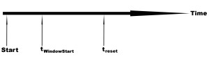
Watchdog Sequence
We can calculate the value of tWindowStart and ttimeout as follows (assuming a 16MHz clock):
tWindowStart = 0.768 * ((WWDG_CRinitial & 0x3f) – WWDG_WR)
and
ttimeout = 0.768 * (WWDG_CR & 0x3f)
where WWDG_CRinitial is the initial value in the WWDG_CR register.
The default reset value for this register is 0x7f which means that the counter can be reset at any time. In this case, a reset will only be generated if the counter drops below 0x40.
One important point to note is that when the window register is used the value written to the counter (WWDG_CR) must be between 0xc0 and 0x7f. This causes the counter to be reset and the counter value to be reset simultaneously.
Software
The function of the Window Watchdog will be illustrated using the following three examples:
- WWDG_CR not reset
- WWDG_CR reset outside the reset window
- WWDG_CR reset inside the reset window
The first thing we need to do is add some code which will be used in all of the examples.
Common Code
Firstly, lets add the code which will be common to all of the examples:
//
//  This program demonstrates how to use the Window Watchdog on the STM8S
//  microcontroller.
//
//  This software is provided under the CC BY-SA 3.0 licence.  A
//  copy of this licence can be found at:
//
//  http://creativecommons.org/licenses/by-sa/3.0/legalcode
//
#include <iostm8S105c6.h>
#include <intrinsics.h>

//--------------------------------------------------------------------------------
//
//  Setup the system clock to run at 16MHz using the internal oscillator.
//
void InitialiseSystemClock()
{
    CLK_ICKR = 0;                       //  Reset the Internal Clock Register.
    CLK_ICKR_HSIEN = 1;                 //  Enable the HSI.
    CLK_ECKR = 0;                       //  Disable the external clock.
    while (CLK_ICKR_HSIRDY == 0);       //  Wait for the HSI to be ready for use.
    CLK_CKDIVR = 0;                     //  Ensure the clocks are running at full speed.
    CLK_PCKENR1 = 0xff;                 //  Enable all peripheral clocks.
    CLK_PCKENR2 = 0xff;                 //  Ditto.
    CLK_CCOR = 0;                       //  Turn off CCO.
    CLK_HSITRIMR = 0;                   //  Turn off any HSIU trimming.
    CLK_SWIMCCR = 0;                    //  Set SWIM to run at clock / 2.
    CLK_SWR = 0xe1;                     //  Use HSI as the clock source.
    CLK_SWCR = 0;                       //  Reset the clock switch control register.
    CLK_SWCR_SWEN = 1;                  //  Enable switching.
    while (CLK_SWCR_SWBSY != 0);        //  Pause while the clock switch is busy.
}

//--------------------------------------------------------------------------------
//
//  Initialise the ports.
//
//  Configure all of Port D for output.
//
void InitialisePorts()
{
    PD_ODR = 0;             //  All pins are turned off.
    PD_DDR = 0xff;          //  All pins are outputs.
    PD_CR1 = 0xff;          //  Push-Pull outputs.
    PD_CR2 = 0xff;          //  Output speeds up to 10 MHz.
}
This code has been used many times in The Way of the Register series of posts. It simply sets the system clock to the high speed internal clock and configures Port D for output.
Example 1 – Continuous Reset
This example sets the Windows Watchdog running and then waits for the watchdog to trigger the system reset. We indicate that the application is running by generating a pulse on Port D, pin 2.
//--------------------------------------------------------------------------------
//
//  Initialise the Windows Watchdog.
//
void InitialiseWWDG()
{
    PD_ODR_ODR2 = 1;
    __no_operation();
    __no_operation();
    __no_operation();
    __no_operation();
    PD_ODR_ODR2 = 0;
    WWDG_CR = 0xc0;
}
The __no_operation() instruction in the above code allow the pulse to stabilise on the pin.
The WWDG_CR is set to 0xc0 to both set the value in the counter and enable the watchdog at the same time. This sets bit 6 in the counter to 11 and the remaining bits to 0 (i.e. the counter is set to 0x40). The effect of this is that the first down count event will cause bit 6 to be cleared and the counter to be set to 0x3f. This will trigger the reset event.
The main program simply sets everything up and then “pauses” by simply waiting for an interrupt:
//--------------------------------------------------------------------------------
//
//  Main program loop.
//
int main()
{
    //
    //  Initialise the system.
    //
    __disable_interrupt();
    InitialiseSystemClock();
    InitialisePorts();
    InitialiseWWDG();
    __enable_interrupt();
    //
    //  Main program loop.
    //
    while (1)
    {
        __wait_for_interrupt();
    }
}
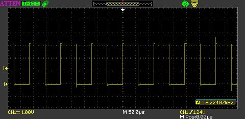
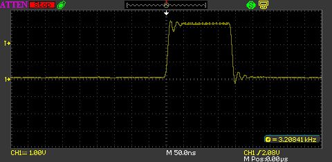
If we run this application and connect PD2 and NRST to the oscilloscope we see the following trace:
Initial continuous reset
The yellow trace shows the reset line being pulled low and gradually returning to high. The drop shows where the watchdog has caused the reset pin to be pulled low and the microcontroller to be reset. The blue trace shows the pulse on PD2. If we measure the time difference between the pulse on PD2 and the time that the reset pin is pulled low we find that this is 770uS. This is very close to the time for one count, 768uS.
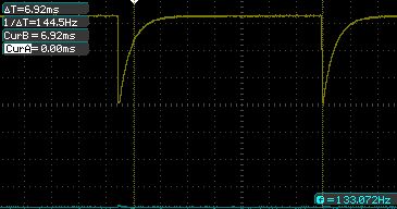
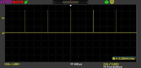
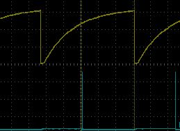
To verify this we can change the value in the counter to say 0x48. In this case we should see the watchdog running for 9 counts and the system running for 6.912mS. Changing
WWDG_CR = 0xc0 to
WWDG_CR = 0xc8 gives the following output on the oscilloscope:
Continuous reset
Measuring the time difference we get a value of 6.9mS.
Example 2 – Reset Outside Watchdog Window
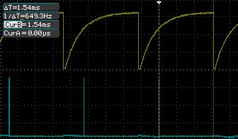
Using the above code as a starting point we will look at the effects of the watch dog window register (WWDG_WR). This defines when the application is allowed to change the value in the counter. The first task is to change the initial value in the control register to 0xc1 and verify that we get a rest every 1.54ms (2 x timer period). So change the InitialiseWWDG method to the following:
void InitialiseWWDG()
{
    PD_ODR_ODR2 = 1;
    __no_operation();
    __no_operation();
    __no_operation();
    __no_operation();
    PD_ODR_ODR2 = 0;
    WWDG_CR = 0xc1;
}
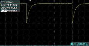
Running this application on the STM8S Discovery board results in the following traces:
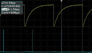
Reset Outside window
Now we have two counts (1.54mS) in order to change the value in the control register. First task is to modify the InitialiseWWDG method to define the window. We will define this to be 0x40:
void InitialiseWWDG()
{
    PD_ODR_ODR2 = 1;
    __no_operation();
    __no_operation();
    __no_operation();
    __no_operation();
    PD_ODR_ODR2 = 0;
    WWDG_CR = 0xc1;
    WWDG_WR = 0x40;
}
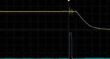
This means that for the first 768uS the control register should not be changed. If the register is changed during this period a reset will be triggered. To demonstrate this we will change the value in the control register immediately after the microcontroller has been initialised:
int main()
{
    //
    //  Initialise the system.
    //
    __disable_interrupt();
    InitialiseSystemClock();
    InitialisePorts();
    InitialiseWWDG();
    __enable_interrupt();
    //
    //  Main program loop.
    //
    while (1)
    {
        WWDG_CR = 0xc1;             //  Trigger a reset.
        __wait_for_interrupt();
    }
}
Deploying this application to the microcontroller results in the following trace on the oscilloscope:

Watchdog immediate reset
As you can see, the system is reset almost immediately (there is virtually no time between the pulse on PD2 and the reset line being pulled low).
Example 3 – Reset Within the Watchdog Window
Starting with the common code we initialise the Window Watchdog with the following method:
//--------------------------------------------------------------------------------
//
//  Initialise the Windows Watchdog.
//
void InitialiseWWDG()
{
    WWDG_CR = 0x5b;         //  Approx 70ms total window.
    WWDG_WR = 0x4c;         //  Approx 11.52ms window where cannot reset
    WWDG_CR_WDGA = 1;       //  Enable the watchdog.
}
This code defines a period of 11.52ms where we cannot reset the window watchdog counter followed by a period of 9.216ms during which the watchdog counter must be reset in order to prevent the microcontroller from being reset.
A simple main application loop would look something like this:
//--------------------------------------------------------------------------------
//
//  Main program loop.
//
int main()
{
    //
    //  Initialise the system.
    //
    __disable_interrupt();
    InitialiseSystemClock();
    InitialisePorts();
    PD_ODR_ODR4 = 1;
    __no_operation();
    PD_ODR_ODR4 = 0;
    InitialiseWWDG();
    __enable_interrupt();
    //
    //  Main program loop.
    //
    while (1)
    {
        unsigned char counter = (unsigned char) WWDG_CR;
        if ((counter & 0x7f) < WWDG_WR)
        {
            WWDG_CR = 0xdb;     //  Reset the Window Watchdog counter.
            PD_ODR_ODR2 = !PD_ODR_ODR2;
        }
        //
        //  Do something here.
        //
    }
}
The initial pulse on PD4 indicates that the application has started. We can use this to detect the reset of the microcontroller. In this trivial application the main program loop simply checks to see if the current value of the counter is less than the value in WWDG_WR. If the counter is less than WWDG_WR then the system write a new value into the counter. The value written is 0x5b anded with 0x80, this brings the reset value into the value range (0xc0 – 0xff).
This application also pulses PD2 to indicate that the watchdog counter has been reset.
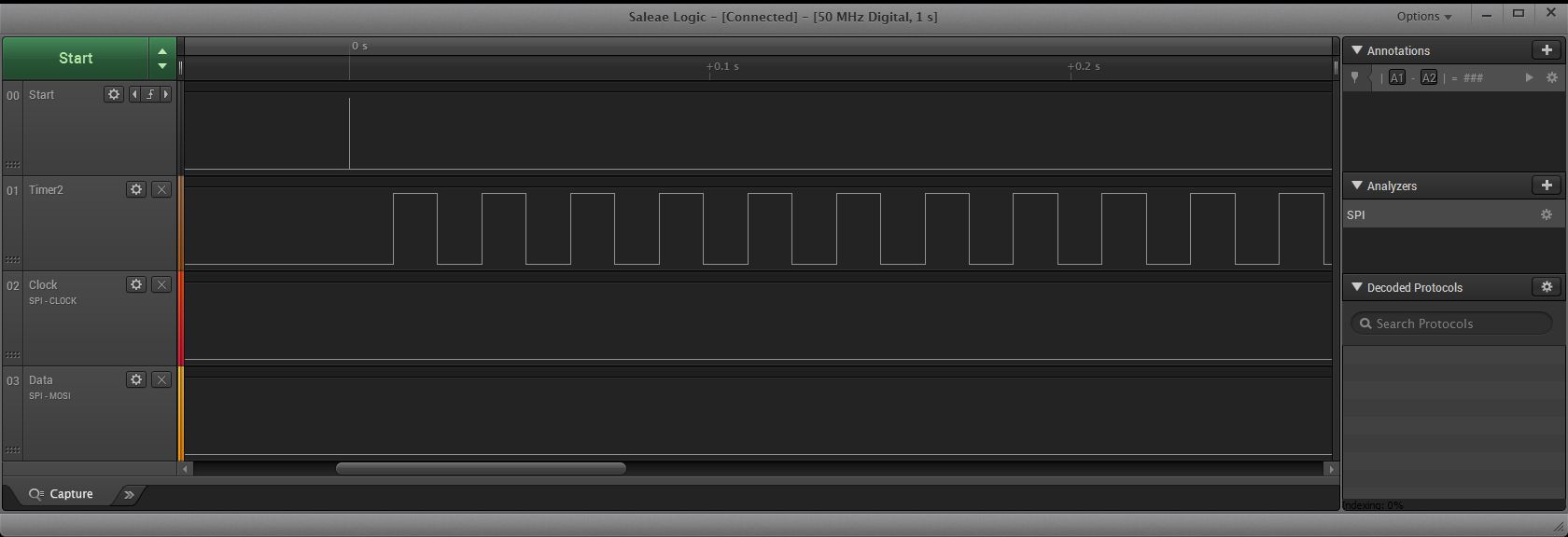
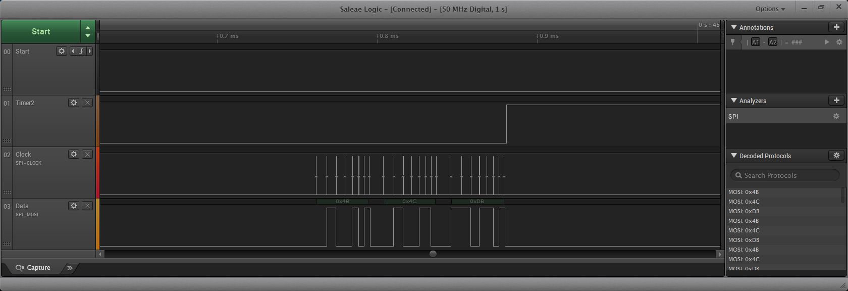
Deploying this application and hooking up the Saleae logic analyser gives the following trace:
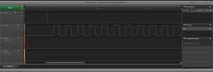
Window watchdog initial trace
As you can see, there is an initial pulse showing that the board is reset (top trace) and then a series of pulses showing that the counter is being reset (lower trace). Each up/down transition represents a watchdog counter reset.
This is a relatively trivial example so let’s spice this up and add in a timer.
To the code above add the following code:
//--------------------------------------------------------------------------------
//
//  Setup Timer 2 to generate a 12.5ms interrupt.
//
void SetupTimer2()
{
    TIM2_PSCR = 0x02;       //  Prescaler = 4.
    TIM2_ARRH = 0xc3;       //  High byte of 50,000.
    TIM2_ARRL = 0x50;       //  Low byte of 50,000.
    TIM2_IER_UIE = 1;       //  Enable the update interrupts.
    TIM2_CR1_CEN = 1;       //  Finally enable the timer.
}
This method will set up timer 2 to generate an interrupt every 12.5ms.
Adding the following will catch the interrupt:
//--------------------------------------------------------------------------------
//
//  Timer 2 Overflow handler.
//
#pragma vector = TIM2_OVR_UIF_vector
__interrupt void TIM2_UPD_OVF_IRQHandler(void)
{
    if (_firstTime)
    {
        InitialiseWWDG();
        _firstTime = 0;
    }
    else
    {
        unsigned char counter = (unsigned char) WWDG_CR;
        unsigned char window = WWDG_WR;
        BitBangByte(counter & 0x7f);
        BitBangByte(window);
        WWDG_CR = 0xdb;     //  Reset the Window Watchdog counter.
        counter = (unsigned char) WWDG_CR;
        BitBangByte(counter);
    }
    PD_ODR_ODR2 = !PD_ODR_ODR2;
    TIM2_SR1_UIF = 0;       //  Reset the interrupt otherwise it will fire again straight away.
}
The interrupt will, on first invocation, initialise the window watchdog. Subsequent invocations will output the values of the registers and reset the window watchdog.
We need some code to bit bang the register values:
#define SR_CLOCK            PD_ODR_ODR5
#define SR_DATA             PD_ODR_ODR3

//
//  BitBang the data through the GPIO ports.
//
void BitBangByte(unsigned char b)
{
    //
    //  Initialise the clock and data lines into known states.
    //
    SR_DATA = 0;                    //  Set the data line low.
    SR_CLOCK = 0;                   //  Set the clock low.
    //
    //  Output the data.
    //
    for (int index = 7; index >= 0; index--)
    {
        SR_DATA = ((b >> index) & 0x01);
        SR_CLOCK = 1;               //  Send a clock pulse.
        __no_operation();
        SR_CLOCK = 0;
    }
    //
    //  Set the clock and data lines into a known state.
    //
    SR_CLOCK = 0;                   //  Set the clock low.
    SR_DATA = 0;
}
The main program loop needs to be modified to set up the timer and registers etc. So replace the main program loop with the following:
//--------------------------------------------------------------------------------
//
//  Main program loop.
//
int main()
{
    //
    //  Initialise the system.
    //
    __disable_interrupt();
    InitialiseSystemClock();
    InitialisePorts();
    PD_ODR_ODR4 = 1;
    __no_operation();
    PD_ODR_ODR4 = 0;
    SetupTimer2();
    InitialiseWWDG();
    __enable_interrupt();
    //
    //  Main program loop.
    //
    while (1)
    {
        __wait_for_interrupt();
    }
}
Deploying and running this application gives the following output on the Saleae logic analyser:
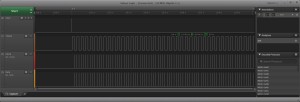
Window watchdog full trace
Zooming in produces the following
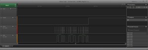
Window watchdog zoomed in
Starting with the top trace and descending we can see the following values:
- Reset pulse
- Timer 2 interrupt triggers (up/down transitions)
- Data (register values)
- Clock signal
The decoded register values can be seen above the data trace. The first value is the current value of the counter. The second value is the value in the window watchdog register and the final value is the new value in the counter register.
Conclusion
The Window Watchdog provides a mechanism for the developer to detect software faults similar to the Independent Watchdog but further constrains the developer by defining a window where a counter reset by the application is not allowed.