Weather Station Proof of Concept Software
Sunday, April 3rd, 2016The weather station project is still at the proof of concept stage but the last few articles have run through the concepts for connecting several sensors to the Digistump Oak microcontroller. In this article we will look at the basic (and I stress basic) software required to connect the sensors discussed so far with the microcontroller and start to collect data.
Hardware – So Far
In the previous articles the following sensors have been discussed:
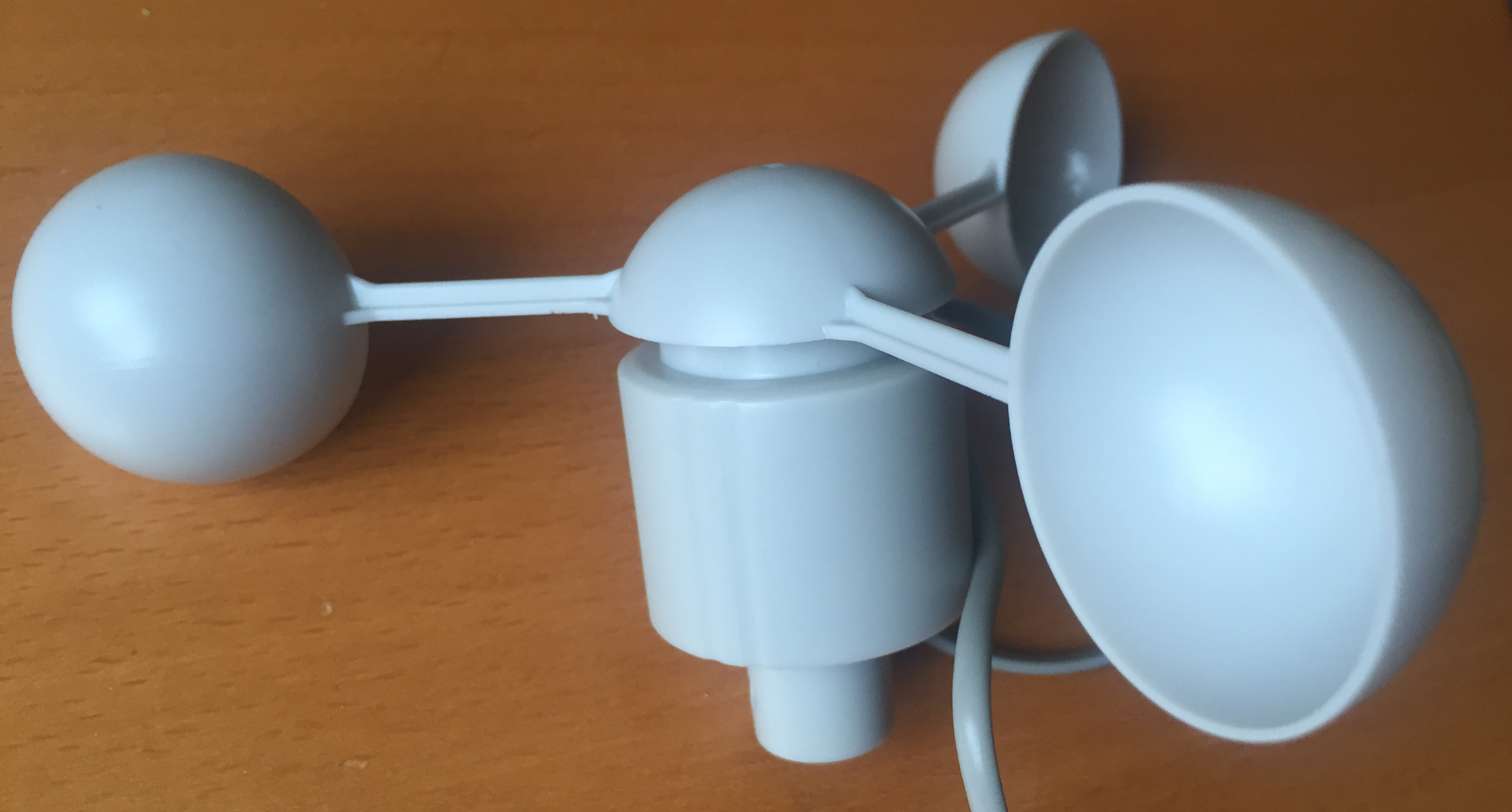
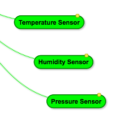
- Weather meter
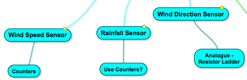
- TSL2561 – Luminosity sensor
- BME280 – Air pressure, temperature and humidity sensor
- ML8511 – Ultraviolet Light Sensor
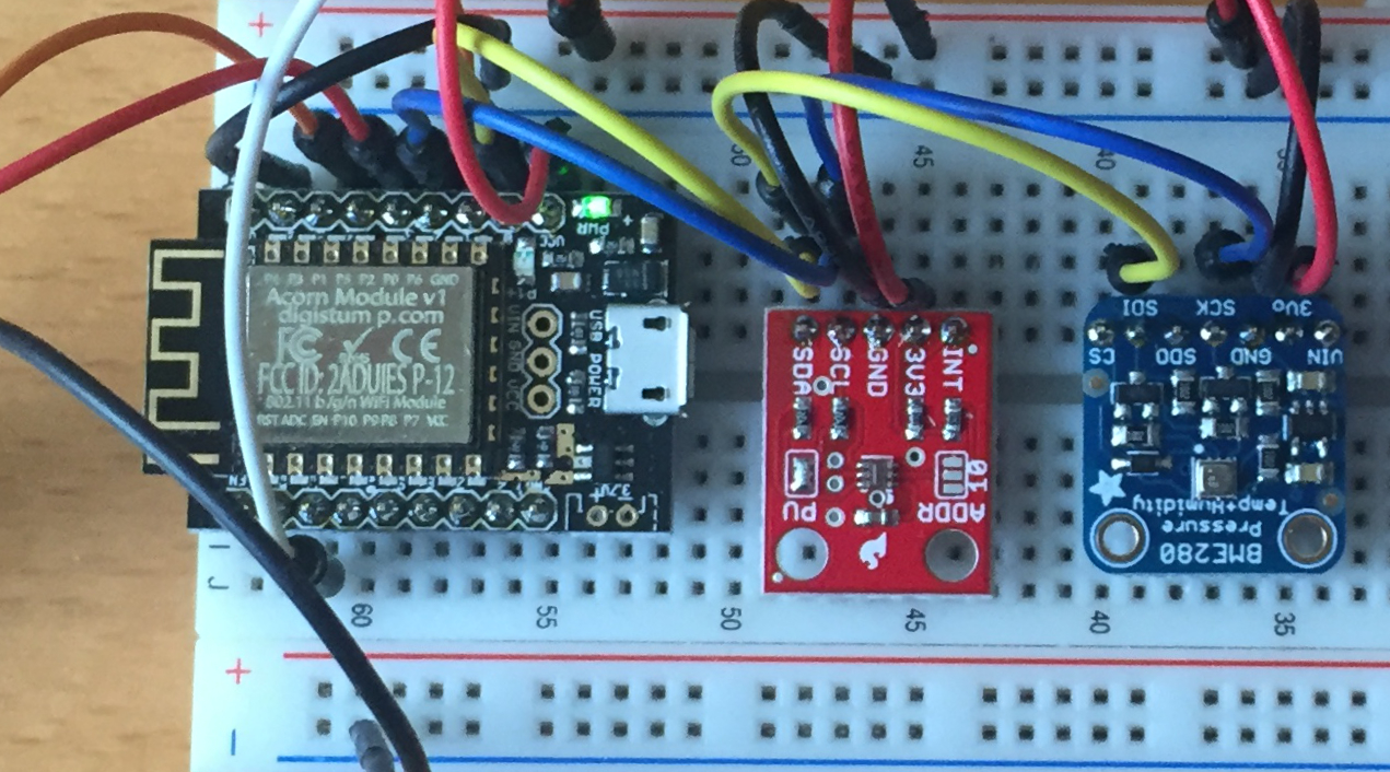
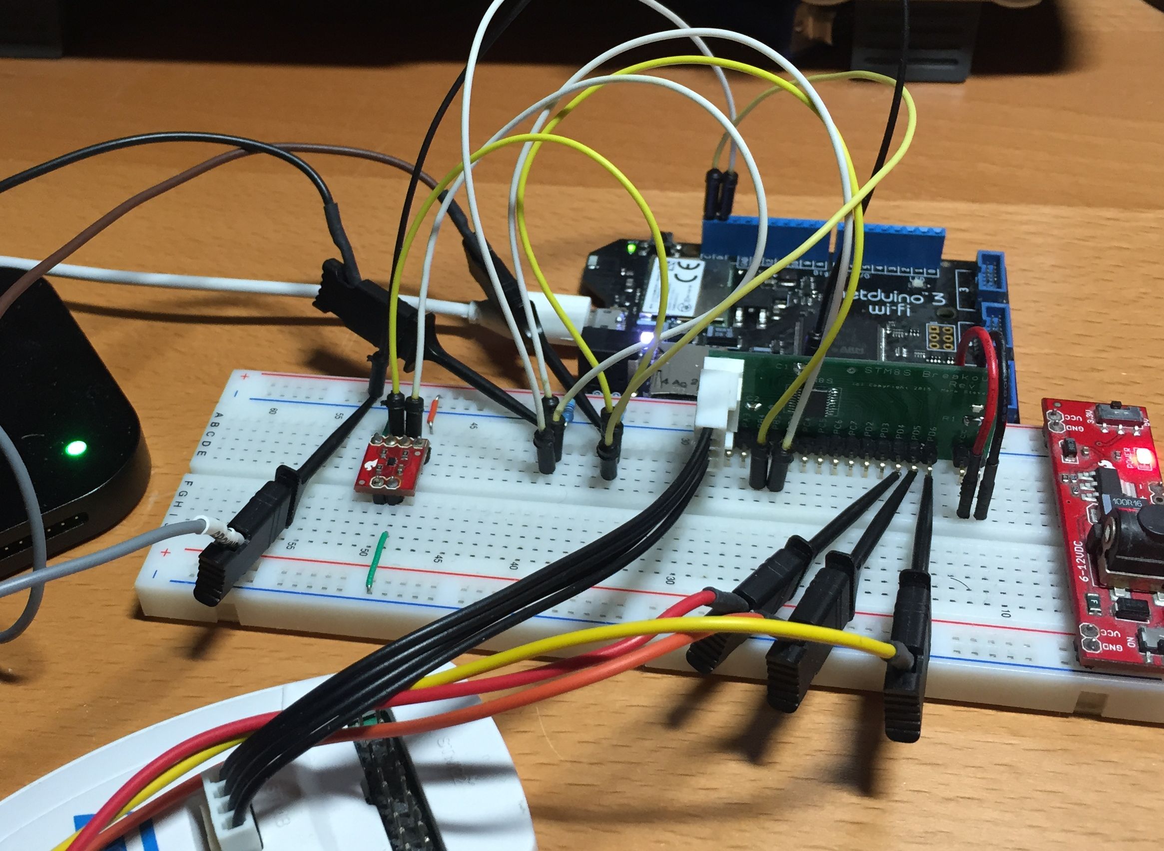
These sensors are currently connected to a piece of breadboard along with the Oak.
Now we have the sensors connected we need to add some software goodness.
Software Requirements
The first and most obvious requirement is to be able to collect data from the above sensors. In addition the proof of concept software should also permit the following:
- Test logging data to the cloud
- Serial debugging
- Setting the system time from the Internet
Data logging to the cloud will initially be to the Sparkfun Data Service as this is a simple enough service to use. One of the first things to do is to create an account / data stream in order to permit this.
Development Environment
The Arduino development environment can be used to program the Oak and it has the advantage that it is available across multiple environments. Digistump recommend using version 1.6.5 of the Arduino environment as there are known issues with more current versions.
Libraries
In previous articles it was noted that Sparkfun and Adafruit provide libraries for two of the I2C sensor boards being used (BME280 and TSL2561). An additional library is also required to support the third objective, setting the time from the Internet.
The additional libraries are installed from the Sketch -> Include Library -> Manage Libraries.. dialog. Open this dialog and install the following libraries:
- Adafruit Unified Sensor (1.0.2)
- Adafruit BME280 (1.0.3)
- Sparkfun TSL2561 (1.1.0)
- NtpClientLib by German Martin (1.3.0)
The version numbers are the ones available at the time of writing.
Software Walk Through
At this point the hardware should be in place and all of the necessary libraries installed. Let the coding begin.
This first thing we need is the includes for the libraries that are going to be used:
#include <ESP8266WiFi.h>
#include <ESP8266HTTPClient.h>
#include <Time.h>
#include <NtpClientLib.h>
#include <SparkFunTSL2561.h>
#include <Adafruit_Sensor.h>
#include <Adafruit_BME280.h>
#include <Wire.h>
#include <SPI.h>
The SPI library is not going to be used in this example but will be required in future articles.
Next up we need some definitions and global variables to support the sensors:
//
//  Definitions used in the code for pins etc.
//
#define VERSION           "0.04"
//
#define PIN_SLEEP_OR_RUN  7
#define PIN_ONBOARD_LED   1
#define PIN_ANEMOMETER    5
#define PIN_PLUVIOMETER   8
//
#define SLEEP_PERIOD      60

//
//  Light sensor (luminosity).
//
SFE_TSL2561 light;

//
//  Create a Temperature, humidity and pressure sensor.
//
Adafruit_BME280 bme;
float temperature;
float pressure;
float humidity;

//
//  TLS2561 related globals.
//
boolean gain;       //  Gain setting, 0 = X1, 1 = X16;
unsigned int ms;    //  Integration ("shutter") time in milliseconds
double lux;         //  Luminosity in lux.
boolean good;       //  True if neither sensor is saturated

//
//  Ultraviolet analog reading.
//
int ultraviolet;
#define UV_GRADIENT           0.12
#define MAXIMUM_ANALOG_VALUE  1023
#define REFERENCE_VOLTAGE     3.3
#define UV_OFFSET             1.025

//
//  Buffer for messages.
//
char buffer[256];
char number[20];

//
//  NTP class to provide system time.
//
ntpClient *ntp;

//
//  Wind Speed sensor, each pulse per second represents 1.492 miles per hour.
//
volatile int windSpeedPulseCount;
#define WINDSPEED_DURATION      5
#define WINDSPEED_PER_PULSE     1.492

//
//  We are logging to Phant and we need somewhere to store the client and keys.
//
#define PHANT_DOMAIN        "data.sparkfun.com"
#define PHANT_PAGE          "/input/---- Your stream ID goes here ----"
const int phantPort = 80;
#define PHANT_PRIVATE_KEY   "---- Your Private Key goes here ----"
Before we progress much further it should be acknowledged that some of the code for the BMS280 and the TSL2561 is modified from the Adafruit and Sparkfun example applications.
A key point to note from the above code is the definition of the windSpeedPulseCount variable. Note the use of the volatile keyword. This tells the compiler not to optimise the use of this variable.
Next up is some support code. Two methods are initially required, ftoa adds the limited ability to convert a floating point number to a char * for debugging. The second method outputs a debugging message. This has been abstracted to allow for possible network debug messages later in the project. At the moment the serial port will be used.
//
//  Output a diagnostic message if debugging is turned on.
//
void DebugMessage(String message)
{
    Serial.println(message);
}

//
//  Convert a float to a string for debugging.
//
char *ftoa(char *a, double f, int precision)
{
    long p[] = {0, 10, 100, 1000, 10000, 100000, 1000000, 10000000, 100000000};

    char *ret = a;
    long integer = (long) f;
    itoa(integer, a, 10);
    while (*a != '\0')
    {
        a++;
    }
    if (precision != 0)
    {
      *a++ = '.';
      long decimal = abs((long) ((f - integer) * p[precision]));
      itoa(decimal, a, 10);
    }
    return ret;
}
TSL2561 – Luminosity Sensor
The next group of methods deal with the luminosity sensor, the TSL2561. these methods are slightly modified versions of the example code from Sparkfun. It is envisaged that future versions of these methods will deal with saturation and low light levels by dynamically changing the way the sensor works. For the proof of concept the basic code should suffice:
//
//  Convert the error from the TSL2561 into an error that a human can understand.
//
void PrintLuminosityError(byte error)
{
    switch (error)
    {
        case 0:
            DebugMessage("TSL2561 Error: success");
            break;
        case 1:
            DebugMessage("TSL2561 Error: data too long for transmit buffer");
            break;
        case 2:
            DebugMessage("TSL2561 Error: received NACK on address (disconnected?)");
            break;
        case 3:
            DebugMessage("TSL2561 Error: received NACK on data");
            break;
        case 4:
            DebugMessage("TSL2561 Error: other error");
            break;
        default:
            DebugMessage("TSL2561 Error: unknown error");
    }
}

//
//  Set up the luminsoity sensor.
//
void SetupLuminositySensor()
{
    light.begin();

    // Get factory ID from sensor:
    // (Just for fun, you don't need to do this to operate the sensor)
    unsigned char id;

    if (light.getID(id))
    {
        sprintf(buffer, "Retrieved TSL2561 device ID: 0x%x", id);
        DebugMessage(buffer);
    }
    else
    {
        byte error = light.getError();
        PrintLuminosityError(error);
    }

    // The light sensor has a default integration time of 402ms,
    // and a default gain of low (1X).

    // If you would like to change either of these, you can
    // do so using the setTiming() command.

    // If gain = false (0), device is set to low gain (1X)
    // If gain = high (1), device is set to high gain (16X)
    gain = 0;

    // If time = 0, integration will be 13.7ms
    // If time = 1, integration will be 101ms
    // If time = 2, integration will be 402ms
    // If time = 3, use manual start / stop to perform your own integration
    unsigned char time = 2;

    // setTiming() will set the third parameter (ms) to the
    // requested integration time in ms (this will be useful later):
    light.setTiming(gain, time, ms);

    // To start taking measurements, power up the sensor:

    DebugMessage((char *) "Powering up the luminosity sensor.");
    light.setPowerUp();
}

//
//  Read the luminosity from the TSL2561 luminosity sensor.
//
void ReadLuminositySensor()
{
    unsigned int data0, data1;

    if (light.getData(data0, data1))
    {
        sprintf(buffer, "TSL2561 data: 0x%04x, 0x%04x", data0, data1);
        DebugMessage(buffer);
        //
        //  To calculate lux, pass all your settings and readings to the getLux() function.
        //
        //  The getLux() function will return 1 if the calculation was successful, or 0 if one or both of the sensors was
        //  saturated (too much light). If this happens, you can reduce the integration time and/or gain.
        //  For more information see the hookup guide at:
        //  https://learn.sparkfun.com/tutorials/getting-started-with-the-tsl2561-luminosity-sensor
        //

        //
        // Perform lux calculation.
        //
        double localLux;
        good = light.getLux(gain ,ms, data0, data1, localLux);
        if (good)
        {
            lux = localLux;
        }
    }
    else
    {
        byte error = light.getError();
        PrintLuminosityError(error);
    }
}

//
//  Log the luminosity data to the debug stream.
//
void LogLuminosityData()
{
    sprintf(buffer, "Lux: %s", ftoa(number, lux, 2));
    DebugMessage(buffer);
}
BME280 – Air Temperature, Pressure and Humidity Sensor
Dealing with this sensor is simpler than the luminosity sensor as can be seen from the code below:
//
//  Setup the Adafruit BME280 Temperature, pressure and humidity sensor.
//
void SetupTemperaturePressureSensor()
{
    if (!bme.begin())
    {
        DebugMessage("Could not find a valid BME280 sensor, check wiring!");
    }
    else
    {
        DebugMessage("BME280 sensor located on I2C bus.");
    }
}

//
//  Log the data from the temperature, pressure and humidity sensor.
//
void LogTemperaturePressureData()
{
    sprintf(buffer, "Temperature: %s C", ftoa(number, temperature, 2));
    DebugMessage(buffer);
    sprintf(buffer, "Humidity: %s %%", ftoa(number, humidity, 2));
    DebugMessage(buffer);
    sprintf(buffer, "Pressure: %s hPa", ftoa(number, pressure / 100, 0));
    DebugMessage(buffer);
}

//
//  Read the data from the Temperature, pressure and humidity sensor.
//
void ReadTemperaturePressureSensor()
{
    temperature = bme.readTemperature();
    pressure = bme.readPressure();
    humidity = bme.readHumidity();
}
This group of methods follows a similar line to the TSL2561 sensor methods, namely, setup, read and log methods.
ML8511 – Ultraviolet Light Sensor
This sensor is the simplest so far as it provides a simple analog value representing the intensity of the ultraviolet light falling on the sensor.
//
//  Read the ultraviolet light sensor.
//
void ReadUltravioletSensor()
{
    ultraviolet = analogRead(A0);
}

//
//  Log the reading from the ultraviolet light sensor.
//
void LogUltravioletData()
{
    char num[20];

    sprintf(buffer, "Ultraviolet light: %s", itoa(ultraviolet, num, 10));
    DebugMessage(buffer);
}
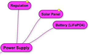
Note that this sensor does allow for an enable line. This can be used to disable the sensor and put it into a low power mode if necessary. This will not be used in the proof of concept will be considered when the project moves to the point where power supplies / solar power is considered.
Wind Speed Sensor Interrupt Service Routine (ISR)
This method looks trivial and it is:
//
//  ISR to count the number of pulses from the anemometer (wind speed sensor).
//
void IncreaseWindSpeedPulseCount()
{
    windSpeedPulseCount++;
}
The non-trivial thing to remember about this code is that the method changes a global variable. The volatile keyword used in the variable definition is necessary to stop the compiler from optimising the global variable as this can have side effects.
Data Logging to Sparkfun’s Data Service
Assuming that we have a WiFi connection then we can log the data collected to the Sparkfun data service (this is based upon Phant).
//
//  Post the data to the Sparkfun web site.
//
void PostDataToPhant()
{
    String url = PHANT_PAGE "?private_key=" PHANT_PRIVATE_KEY "&airpressure=";
    url += ftoa(number, pressure / 100, 0);
    url += "&groundmoisture=0";
    url += "&groundtemperature=0";
    url += "&temperature=";
    url += ftoa(number, temperature, 2);
    url += "&humidity=";
    url += ftoa(number, humidity, 2);
    url += "&luminosity=";
    url += ftoa(number, lux, 2);
    url += "&rainfall=0";
    double uvStrength = (((double) ultraviolet) / MAXIMUM_ANALOG_VALUE) * REFERENCE_VOLTAGE;
    if (uvStrength < UV_OFFSET)
    {
        uvStrength = 0;
    }
    else
    {
        uvStrength = (uvStrength - UV_OFFSET) / UV_GRADIENT;
    }
    url += "&ultravioletlight=";
    url += ftoa(number, uvStrength, 2);
    url += "&winddirection=0";
    double windSpeed = windSpeedPulseCount / WINDSPEED_DURATION;
    windSpeed *= WINDSPEED_PER_PULSE;
    url += "&windspeed=";
    url += ftoa(number, windSpeed, 2);
    //
    //  Send the data to Phant (Sparkfun's data logging service).
    //
    HTTPClient http;
    http.begin(PHANT_DOMAIN, phantPort, url);
    int httpCode = http.GET();
    sprintf(buffer, "Status code: %d", httpCode);
    DebugMessage(buffer);
    String response = http.getString();
    sprintf(buffer, "Phant response code: %c", response[3]);
    DebugMessage(buffer);
    if (response[3] != '1')
    {
        //
        //  Need to put some error handling here.
        //
    }
    http.end();
}
The stream has been set up to collect more data than is currently collected, for instance, ground temperature. Any parameter not measured at the moment is set to 0.
Some other things to consider following the proof of concept:
- Error handling for network issues
- Possible offline collection of data
- Using a local version of Phant
Something to bear in mind after the project moved from proof of concept.
Data Collection
The majority of the sensor have a read method to collect the data from the sensor. The only exception at the moment is the wind speed sensor. The data collection is performed inside the main method for collecting and logging the sensor readings:
//
//  Raad the sensors and publish the data.
//
void ReadAndPublishSensorData()
{
    digitalWrite(1, HIGH);
    DebugMessage("\r\nCurrent time: " + ntp->getTimeString());
    ReadLuminositySensor();
    ReadTemperaturePressureSensor();
    LogLuminosityData();
    LogTemperaturePressureData();
    ReadUltravioletSensor();
    LogUltravioletData();
    //
    //  Read the current wind speed.
    //
    DebugMessage("Reading wind speed.");
    windSpeedPulseCount = 0;
    attachInterrupt(PIN_ANEMOMETER, IncreaseWindSpeedPulseCount, RISING);
    delay(WINDSPEED_DURATION * 1000);
    detachInterrupt(PIN_ANEMOMETER);
    //
    PostDataToPhant();
    digitalWrite(1, LOW);
}
Reading the wind speed is performed through the ISR described above. The algorithm is simple:
- Clear the count of the number of revolutions (pulses) from the sensor
- Attach an interrupt to the sensor (the interrupts increments the count every revolution of the sensor)
- Wait for a know number of seconds (in this case 5)
- Detach the interrupt to stop the count
By using this method we can provide an average over a number of seconds and the wind speed can be calculated as:
Wind Speed = (Revolution count / number of seconds) * 1.492
This is the calculation performed in the PostDataToPhant method.
Setup and Loop
The final things needed by an application developed in the Arduino environment are the setup and loop methods. So let’s start looking at the setup method.
//
//  Setup the application.
//
void setup()
{
    Serial.begin(9600);
    Serial.println("\r\n\r\n-----------------------------\r\nWeather Station Starting (version " VERSION ", built: " __TIME__ " on " __DATE__ ")");
    Serial.println();
    //
    //  Connect to the WiFi.
    //
    Serial.print("\r\nConnecting to default network");
At the start of setup we need to rely upon the Serial object being available and so there are no calls to the DebugMessage method as this may be modified later to use networking for debugging. The next step is to try and connect to the network:
    WiFi.begin();
    while (WiFi.status() != WL_CONNECTED)
    {
      delay(500);
      Serial.print(".");
    }
    Serial.println("");
    Serial.print("WiFi connected, IP address: ");
    Serial.println(WiFi.localIP());
At this point the application will be either looping indefinitely until the network becomes available or we will have an IP address output to the serial port. In a more complete application this will start the logging process and periodically try to connect to the network when the network is unavailable. This is only a proof of concept after all.
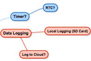
There is currently no Real Time Clock (RTC) attached to the system and so we need to check the network time at startup.
    //
    //  Get the current date and time from a time server.
    //
    DebugMessage("Setting time.");
    ntp = ntpClient::getInstance("time.nist.gov", 0);
    ntp->setInterval(1, 1800);
    delay(1000);
    ntp->begin();
    while (year(ntp->getTime()) == 1970)
    {
        delay(50);
    }
This block of code loops until the network time is set correctly. At start up the year will be set to a default value of 1970, this is why the code loops until the year is something other than 1970.
Next up, setup the sensors and take our first reading:
    //
    //  Set up the sensors and digital pins.
    //
    SetupLuminositySensor();
    SetupTemperaturePressureSensor();
    pinMode(PIN_ONBOARD_LED, OUTPUT);
    pinMode(PIN_ANEMOMETER, INPUT);
    //
    //  Read the initial data set and publish the results.
    //
    ReadAndPublishSensorData();
}
Everything is setup, only thing left is to continue to collect and publish the data, enter loop:
//
//  Main program loop.
//
void loop()
{
    delay(SLEEP_PERIOD * 1000);
    ReadAndPublishSensorData();
}
Example Output
Running the above code results in the following output in the serial monitor (note that some data (IP addresses has been modified):
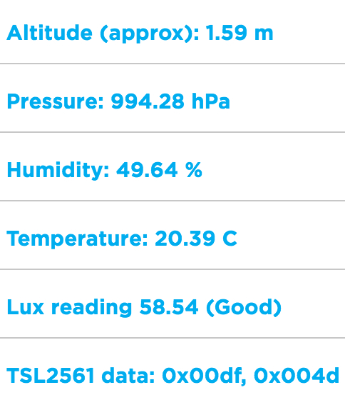
—————————– Weather Station Starting (version 0.04, built: 06:46:39 on Apr 3 2016) Connecting to default network……….. WiFi connected, IP address: 192.168.xxx.yyy Setting time. Retrieved TSL2561 device ID: 0x50 Powering up the luminosity sensor. BME280 sensor located on I2C bus. Current time: 06:48:45 03/04/2016 TSL2561 data: 0x0373, 0x004f Lux: 399.65 Temperature: 18.89 C Humidity: 52.86 % Pressure: 1006 hPa Ultraviolet light: 307 Reading wind speed. Status code: 200 Phant response code: 1The current public data stream for this service should be viewable here.
Checking this stream you can see the resulting data that was sent to Sparkfun for the above serial output:
Phant Data From Weather Station Proof of Concept
One thing to remember when comparing the above data is that the Sparkfun data stream logs data using UTC and the application above was running during British Summer Time.
Conclusion
The code above is a proof of concept, it is not error proof nor does it take into account power usage or optimisation, it is merely meant to prove that the sensors can be read and the data output to a cloud service.
Next steps for the proof of concept:
- How to handle two sensors requiring an analog conversion
- The project is running out of digital pins
- Real time clocks
- Offline data logging
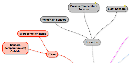
All of this before even looking at the location and powering the project in the wild (OK, my garden).
Back right after this break…