RSS

Archive for September, 2013

Making the D70 Remote More Permanent

Sunday, September 29th, 2013

Now that we have the major components of the Nikon D70 Remote Control unit in place it is about time the unit moved from breadboard to a more permanent home. The last day or two has seen the unit move from breadboard to protoboard.

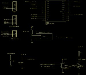
The layout is nothing too complex and at this point I am not too worried about the physical dimensions of the board. So the task at hand is to convert the following schematic into a working board:

Nikon D70 Remote Control Schematic

Nikon D70 Remote Control Schematic

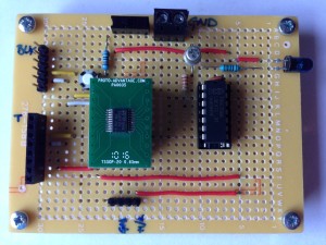
There are plenty of resources out there discussing the techniques for putting together a prototype board from a schematic so we won’t cover these here. Only thing to do is dive in with some Photos starting with the top of the board with the IC’s in place:

Nikon D70 Protoboard Upper

Nikon D70 Protoboard Upper

The eagle eyed amongst you may have noticed that I used a 16-pin DIP socket for the AND gates when I should really have used a 14-pin socket. A little solder soon fixed that problem.

The connectors on the right hand side of the board provide the serial connections by FTDI (upper male connector) and RedBear BLE Mini (lower female connector). The connection at the bottom of the board is the STLink/V2 connector.

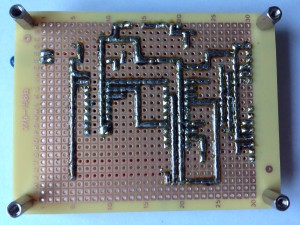
And the bottom of the board:

Nikon D70 Protoboard Lower

Nikon D70 Protoboard Lower

Conclusion

Building the board was not too difficult. The code for the STM8S needed a small modification to move the application from the STM8S105 on the Discovery board to the STM8S103F3 which I have on the DIP to protoboard converter.

Next steps:

  • Allow the EEPROM to be reprogrammed by UART
  • Add support for programmable intervals
  • Consider making the unit standalone (selectable intervals, status display)
  • iPhone application using the RedBear BLE Mini to control the unit

If all goes well it may even end up with a PCB being manufactured and a 3D printed case being made.

Forgot to mention, it still triggers the camera.

Nikon D70 Remote Control with a Button and EEPROM

Thursday, September 12th, 2013

A remote control which can only generate a signal when initially powered up is of limited use. The addition of a switch will allow the user to determine when the camera is triggered.

Adding a Button

The initial versions of the infra-red remote control for the Nikon D70 which have been discussed so far are limited in that the control sequence is transmitted when the STM8S starts and never again until the next time the STM8S is restarted/reset. Adding a button to the remote control will allow the user to select when the control sequence is transmitted.

One of the main problems with switches is that they are subject to switch bounce. You can see an example of this in the post regarding External Interrupts on the STM8S. There are two approaches to switch debouncing, software and hardware. The button on the infra-red remote control will be triggering a sequence of pulses which will typically last several milliseconds. This means that it lends itself to software debouncing using a simple state machine.

The state machine will put the infra-red remote control into two states, waiting for user input and running. When waiting for user input the interrupt handler for the switch will accept user input. When in the running mode the system will be generating the infra-red output for the camera and it will ignore any input from the switch. At the end of the infra-red sequence the switch input will be re-enabled.

So much for the theory, lets have a look at the code. The first thing which the application will need to do is to setup the appropriate pin as an interrupt port:

//--------------------------------------------------------------------------------
//
//  Now set up the ports.
//
//  PD3 - IR Pulse signal.
//  PD4 - Input pin indicating that the user wishes to trigger the camera.
//
void SetupPorts()
{
    PD_ODR = 0;             //  All pins are turned off.
    //
    //  PD3 is the output for the IR control.
    //
    PD_DDR_DDR3 = 1;
    PD_CR1_C13 = 1;
    PD_CR2_C23 = 1;
    //
    //  Now configure the input pin.
    //
    PD_DDR_DDR4 = 0;        //  PD4 is input.
    PD_CR1_C14 = 1;         //  PD4 is floating input.
    PD_CR2_C24 = 1;
    //
    //  Set up the interrupt.
    //
    EXTI_CR1_PDIS = 1;      //  Interrupt on rising edge.
    EXTI_CR2_TLIS = 1;      //  Rising edge only.
}

The modifications to the SetupPorts method keeps the infra-red output on PD3 but adds an input on PD4 with a rising edge interrupt.

The next step is to deal with the interrupt on PD4. Here we need to work out if we are waiting for an interrupt and if we are then the application needs to start the generation of the infra-red signal. If we are not waiting for a button press then we should ignore the user request as it is likely to be a result of switch bounce. The code starts to look like this:

//--------------------------------------------------------------------------------
//
//  Process the interrupt generated by the pressing of the button.
//
//  This ISR makes the assumption that we only have on incoming interrupt on Port D.
//
#pragma vector = 8
__interrupt void EXTI_PORTD_IRQHandler(void)
{
    if (_currentState != STATE_RUNNING)
    {
        //
        //  Set everything up ready for the timers.
        //
        
        //  TODO!
        
        //
        //  Now we have everything ready we need to force the Timer 2 counters to
        //  reload and enable Timers 1 & 2.
        //
        TIM2_CR1_URS = 1;
        TIM2_EGR_UG = 1;
        TIM1_CR1_CEN = 1;
        TIM2_CR1_CEN = 1;
    }
}

The exact code required for setting up the timer will be revealed following the EEPROM section of this post.

Using EEPROM

In the post Storing Data in the EEPROM on the STM8S we saw how we could save data into the EEPROM of the STM8S for later retrieval. The data used in the example should look familiar if you have been following this series on the Nikon D70 Remote Control as it is the timing and signal data which triggers the Nikon D70.

The first thing we should do is to modify the order in which the data is written into the EEPROM. In the above post, the timing data is written into the EEPROM low byte followed by high byte. By swapping the order we can store the data in the order required by the interrupt for Timer 2. So the first task is to modify the application which wrote and verified the timing information to the following:

//
//  Write a series of bytes to the EEPROM of the STM8S105C6 and then
//  verify that the data has been written correctly.
//
//  This software is provided under the CC BY-SA 3.0 licence.  A
//  copy of this licence can be found at:
//
//  http://creativecommons.org/licenses/by-sa/3.0/legalcode
//
#if defined DISCOVERY
    #include <iostm8S105c6.h>
#else
    #include <iostm8s103f3.h>
#endif

//
//  Data to write into the EEPROM.
//
unsigned int _pulseLength[] = { 2000U, 27830U, 400U, 1580U, 400U, 3580U, 400U };
unsigned char _onOrOff[] =    {   1,      0,     1,     0,    1,     0,    1 };
char numberOfValues = 7;

//--------------------------------------------------------------------------------
//
//  Write the default values into EEPROM.
//
void SetDefaultValues()
{
    //
    //  Check if the EEPROM is write-protected.  If it is then unlock the EEPROM.
    //
    if (FLASH_IAPSR_DUL == 0)
    {
        FLASH_DUKR = 0xae;
        FLASH_DUKR = 0x56;
    }
    //
    //  Write the data to the EEPROM.
    //
    char *address = (char *) 0x4000;        //  EEPROM base address.
    *address++ = (char) numberOfValues;
    for (int index = 0; index < numberOfValues; index++)
    {
        *address++ = (char) ((_pulseLength[index] >> 8) & 0xff);
        *address++ = (char) (_pulseLength[index] & 0xff);
        *address++ = _onOrOff[index];
    }
    //
    //  Now write protect the EEPROM.
    //
    FLASH_IAPSR_DUL = 0;
}

//--------------------------------------------------------------------------------
//
//  Verify that the data in the EEPROM is the same as the data we
//  wrote originally.
//
void VerifyEEPROMData()
{
    PD_ODR_ODR2 = 1;            //  Checking the data
    PD_ODR_ODR3 = 0;            //  No errors.
    //
    char *address = (char *) 0x4000;        //  EEPROM base address.
    if (*address++ != numberOfValues)
    {
        PD_ODR_ODR3 = 1;
    }
    else
    {
        for (int index = 0; index < numberOfValues; index++)
        {
            unsigned int value = (*address++ << 8);
            value += *address++;
            if (value != _pulseLength[index])
            {
                PD_ODR_ODR3 = 1;
            }
            if (*address++ != _onOrOff[index])
            {
                PD_ODR_ODR3 = 1;
            }
        }
    }
    PD_ODR_ODR2 = 0;        // Finished processing.
}

//--------------------------------------------------------------------------------
//
//  Setup port D for data output.
//
void SetupPorts()
{
    //
    //  Initialise Port D.
    //
    PD_ODR = 0;             //  All pins are turned off.
    PD_DDR = 0xff;          //  All bits are output.
    PD_CR1 = 0xff;          //  All pins are Push-Pull mode.
    PD_CR2 = 0xff;          //  Pins can run up to 10 MHz.
}

//--------------------------------------------------------------------------------
//
//  Main program loop.
//
void main()
{
    SetupPorts();
    SetDefaultValues();
    VerifyEEPROMData();
}

Create a new project for the above and execute the program on the STM8S Discovery board. This should set up the timing data ready for use to use.

Using the EEPROM Data

The above application has been tailored to write the byte data into the EEPROM in the order in which the bytes are required by the remote control application. Using this data should be a simple case of setting a pointer to the first byte and then consuming the bytes one after another. To do this we will need some pointers and a counter:

//
//  Define where we will be working in the EEPROM.
//
#define EEPROM_BASE_ADDRESS         0x4000
#define EEPROM_INITIAL_OFFSET       0x0000
#define EEPROM_DATA_START           (EEPROM_BASE_ADDRESS + EEPROM_INITIAL_OFFSET)

//
//  Data ready for the pulse timer ISR's to use.
//
int _numberOfPulses = 0;
int _currentPulse = 0;
char *_pulseDataAddress = NULL;

As part of the initialisation process we will need to set the pointer and also the number of pulses we have data for:

_pulseDataAddress = (char *) EEPROM_DATA_START;
_numberOfPulses = *_pulseDataAddress++;

So now we should have the initial state configured and we should revisited the button handler method. This method kicks off the timers by consuming the first three bytes of data:

//--------------------------------------------------------------------------------
//
//  Process the interrupt generated by the pressing of the button.
//
//  This ISR makes the assumption that we only have on incoming interrupt on Port D.
//
#pragma vector = 8
__interrupt void EXTI_PORTD_IRQHandler(void)
{
    if (_currentState != STATE_RUNNING)
    {
        //
        //  Set everything up ready for the timers.
        //
        _currentState = STATE_RUNNING;
        _currentPulse = 0;
        _pulseDataAddress = (char *) (EEPROM_DATA_START + 1);
        TIM2_ARRH = *_pulseDataAddress++;
        TIM2_ARRL = *_pulseDataAddress++;
        PD_ODR_ODR3 = *_pulseDataAddress++;
        //
        //  Now we have everything ready we need to force the Timer 2 counters to
        //  reload and enable Timers 1 & 2.
        //
        TIM2_CR1_URS = 1;
        TIM2_EGR_UG = 1;
        TIM1_CR1_CEN = 1;
        TIM2_CR1_CEN = 1;
    }
}

Finally, the interrupt for the Timer 2 interrupt needs to be modified in order to continue to process the data three bytes at a time until we have reached the total number of pulses:

//--------------------------------------------------------------------------------
//
//  Timer 2 Overflow handler.
//
#pragma vector = TIM2_OVR_UIF_vector
__interrupt void TIM2_UPD_OVF_IRQHandler(void)
{
    _currentPulse++;
    if (_currentPulse == _numberOfPulses)
    {
        //
        //  We have processed the pulse data so stop now.
        //
        PD_ODR_ODR3 = 0;
        TIM2_CR1_CEN = 0;
        TIM1_CR1_CEN = 0;           //  Stop Timer 1.
        _currentState = STATE_WAITING_FOR_USER;
    }
    else
    {
        TIM2_ARRH = *_pulseDataAddress++;
        TIM2_ARRL = *_pulseDataAddress++;
        PD_ODR_ODR3 = *_pulseDataAddress++;
        TIM2_CR1_URS = 1;
        TIM2_EGR_UG = 1;
    }
    TIM2_SR1_UIF = 0;               //  Reset the interrupt otherwise it will fire again straight away.
}

Conclusion

The addition of the button certainly makes the remote control more usable as the user can elect when to trigger the camera. At this stage, the EEPROM does not offer too many advantages over the use of the static data but it can allow the remote control to be fine-tuned at a later stage.

The acid test, does it still trigger the camera – Yes it does.

Storing Data in EEPROM on the STM8S

Thursday, September 12th, 2013

During a recent project it became desirable to store a small amount of data in some non-volatile memory in order that the system state could be restored following loss of power. This article demonstrates how to achieve this by writing a small amount of data to the data EEPROM of the STM8S105Cr micro-controller on the STM8S Discovery board.

Memory Layout, Access and Protection

The Data EEPROM area of the STM8S series of micro-controllers varies depending upon the specific unit being used. For this article the specific micro-controller being used is the STM8S105C6 on the STM8S Discovery board. This micro-controller has 1KByte of EEPROM in the address range 0x4000 – 0x43ff.

By default the data area is write protected and cannot be modified by the main program. The write protection is removed by using a key to unlock the EEPROM data area. The flash program area is similarly protected but we will only consider the data EEPROM area. In order to write to the EEPROM area the application will need to write two security keys called Memory Access Security System (MASS) keys to the FLASH_DUKR register. These keys will unlock the EEPROM area and allow the application to write data to the EEPROM until the application turns write protection back on.

The MASS keys for the data EEPROM area are:

  • 0xae
  • 0x56
  • The algorithm for enabling write access to the EEPROM data area is as follows:

    • Check the DUL bit of FLASH_IASPR. If this bit is set then the data area is writeable and no further action is required.
    • Write the first MASS key (0xae) to the FLASH_DUKR register.
    • Write the second MASS key (0x56) to the FLASH_DUKR register.

    At the end of the process of successfully writing the MASS keys the DUL bit of the FLASH_IASPR register will be set. This bit will remain set until either the application changes the bit or the micro-controller is reset. Resetting the DUL bit programatically reinstates the write protection for the EEPROM memory.

    Read-while-write (RWW)

    This feature is not available on all of the STM8S family of processors and you should consult the data sheet for the unit being used if you are interested in using this feature. The RWW feature allows the program memory to be read whilst the EEPROM memory is being written to.

    Byte Programming

    Byte level programming is available for both the program memory and the EEPROM memory. To use this feature the application simply needs to unlock the EEPROM using the MASS keys and then write individual bytes into the EEPROM memory. To erase a byte simply write 0x00 into the memory location.

    Word and Page Programming

    The STM8S also allows word (4 bytes) and block programming. Both of these are faster than byte programming and block programming is faster than word programming. These features will not be discussed further here and are mentioned simply for awareness.

    Interrupts

    The system can be configured to generate an interrupt for the following event:

    • Successful write operation.
    • Successful erase operation.
    • Illegal operation (writing to protected pages).

    Interrupts are enabled by setting FLASH_CR1_IE to 1. When this bit is set, an interrupt will be generated when the FLASH_IASPR_EOP or FLASH_IASPR_WR_PG_DIS bits are set.

    Software

    The original aim of the software was to write a small amount of data to the data EEPROM of the STM8S and use the ST Visual Programmer to verify that the memory contents had changed. As the project progressed it became apparent that we would also need some code to verify the data.

    Writing the Data

    The application to write data to the EEPROM is relatively simple:

    //
    //  Write a series of bytes to the EEPROM of the STM8S105C6.
    //
    //  This software is provided under the CC BY-SA 3.0 licence.  A
    //  copy of this licence can be found at:
    //
    //  http://creativecommons.org/licenses/by-sa/3.0/legalcode
    //
    #if defined DISCOVERY
        #include <iostm8S105c6.h>
    #else
        #include <iostm8s103f3.h>
    #endif
    
    //
    //  Data to write into the EEPROM.
    //
    unsigned int _pulseLength[] = { 2000U, 27830U, 400U, 1580U, 400U, 3580U, 400U };
    unsigned char _onOrOff[] =    {   1,      0,     1,     0,    1,     0,    1 };
    char numberOfValues = 7;
    
    //--------------------------------------------------------------------------------
    //
    //  Write the default values into EEPROM.
    //
    void SetDefaultValues()
    {
        //
        //  Check if the EEPROM is write-protected.  If it is then unlock the EEPROM.
        //
        if (FLASH_IAPSR_DUL == 0)
        {
            FLASH_DUKR = 0xae;
            FLASH_DUKR = 0x56;
        }
        //
        //  Write the data to the EEPROM.
        //
        char *address = (char *) 0x4000;        //  EEPROM base address.
        *address++ = (char) numberOfValues;
        for (int index = 0; index < numberOfValues; index++)
        {
            *address++ = (char) (_pulseLength[index] & 0xff);
            *address++ = (char) ((_pulseLength[index] >> 8) & 0xff);
            *address++ = _onOrOff[index];
        }
        //
        //  Now write protect the EEPROM.
        //
        FLASH_IAPSR_DUL = 0;
    }
    
    //--------------------------------------------------------------------------------
    //
    //  Main program loop.
    //
    void main()
    {
        SetDefaultValues();
    }
    

    The application simply enables writing to the EEPROM and then writes data to the memory. It also re-enables the write protection at the end of the write operation.

    Verifying the Data

    Testing this application should simply be a case of creating a new project, putting the above in main.c, setting some options and then running the code. The EEPROM data can then be read by ST Visual Develop and verified by hand. After compiling and executing the above code, start ST visual Programmer, connect it to the STM8S Discovery board and download the contents of the EEPROM:

    This does not look correct. Double checking the code against RM0016 – Reference Manual all looks good with the application. So try downloading the EEPROM data again:

    This time the data looks good and the values appear to be correct.

    Downloading the EEPROM data again gave the first set of results. Trying for a fourth thime gave the second set of results. It appears that the correct data is only retrieved every second attempt (for reference, I am using ST Visual Develop version 3.2.8 on Windows 8).

    At this point I decided that the only way to ensure that the data is in fact correct is to write a verification method into the code. The new application becomes:

    //
    //  Write a series of bytes to the EEPROM of the STM8S105C6 and then
    //  verify that the data has been written correctly.
    //
    //  This software is provided under the CC BY-SA 3.0 licence.  A
    //  copy of this licence can be found at:
    //
    //  http://creativecommons.org/licenses/by-sa/3.0/legalcode
    //
    #if defined DISCOVERY
        #include <iostm8S105c6.h>
    #else
        #include <iostm8s103f3.h>
    #endif
    
    //
    //  Data to write into the EEPROM.
    //
    unsigned int _pulseLength[] = { 2000U, 27830U, 400U, 1580U, 400U, 3580U, 400U };
    unsigned char _onOrOff[] =    {   1,      0,     1,     0,    1,     0,    1 };
    char numberOfValues = 7;
    
    //--------------------------------------------------------------------------------
    //
    //  Write the default values into EEPROM.
    //
    void SetDefaultValues()
    {
        //
        //  Check if the EEPROM is write-protected.  If it is then unlock the EEPROM.
        //
        if (FLASH_IAPSR_DUL == 0)
        {
            FLASH_DUKR = 0xae;
            FLASH_DUKR = 0x56;
        }
        //
        //  Write the data to the EEPROM.
        //
        char *address = (char *) 0x4000;        //  EEPROM base address.
        *address++ = (char) numberOfValues;
        for (int index = 0; index < numberOfValues; index++)
        {
            *address++ = (char) (_pulseLength[index] & 0xff);
            *address++ = (char) ((_pulseLength[index] >> 8) & 0xff);
            *address++ = _onOrOff[index];
        }
        //
        //  Now write protect the EEPROM.
        //
        FLASH_IAPSR_DUL = 0;
    }
    
    //--------------------------------------------------------------------------------
    //
    //  Verify that the data in the EEPROM is the same as the data we
    //  wrote originally.
    //
    void VerifyEEPROMData()
    {
        PD_ODR_ODR2 = 1;            //  Checking the data
        PD_ODR_ODR3 = 0;            //  No errors.
        //
        char *address = (char *) 0x4000;        //  EEPROM base address.
        if (*address++ != numberOfValues)
        {
            PD_ODR_ODR3 = 1;
        }
        else
        {
            for (int index = 0; index < numberOfValues; index++)
            {
                unsigned int value = *address++;
                value += (*address++ << 8);
                if (value != _pulseLength[index])
                {
                    PD_ODR_ODR3 = 1;
                }
                if (*address++ != _onOrOff[index])
                {
                    PD_ODR_ODR3 = 1;
                }
            }
        }
        PD_ODR_ODR2 = 0;        // Finished processing.
    }
    
    //--------------------------------------------------------------------------------
    //
    //  Setup port D for data output.
    //
    void SetupPorts()
    {
        //
        //  Initialise Port D.
        //
        PD_ODR = 0;             //  All pins are turned off.
        PD_DDR = 0xff;          //  All bits are output.
        PD_CR1 = 0xff;          //  All pins are Push-Pull mode.
        PD_CR2 = 0xff;          //  Pins can run up to 10 MHz.
    }
    
    //--------------------------------------------------------------------------------
    //
    //  Main program loop.
    //
    void main()
    {
        SetupPorts();
        SetDefaultValues();
        VerifyEEPROMData();
    }
    

    The application uses Port D, pins 2 and 3 to indicate how the verification is proceeding. Pin D2 goes high when the application is verifying the data. Pin D3 is used to indicate if an error is found. Compiling the above and connecting up a scope gives the following output:

    Pin D2 is connected to the yellow channel and pin D3 is connected to the blue channel. The above shows that the verification process starts and no errors are generated.

    Conclusion

    There may only be a small amount of EEPROM storage space available on the STM8S (640 bytes to be precise) but this offers a quick and simple method of storing data which may be needed between system resets/power loses.

    In it’s simplest form, the code required to store the data is trivial only requiring the developer to enable the write operations and then disable after the data has been written successfully.

    In addition to the above I would recommend that some form of checksum value is written into the EEPROM as it is possible that the power is lost as the data is being written into the EEPROM. In this case there are two arrays being written and we may only have written half of the data when the power is lost. This is left as an exercise for the reader.

Modulated Nikon D70 Remote Control Signal

Sunday, September 8th, 2013

A quiet Sunday here in the North of England so I decided to add the 38.4KHz modulation to the Nikon D70 Infra-red Remote Control.

I considered two methods of modulating the signal:

  • Software implementation using a timer
  • Hardware implementation using PWM

The software implementation is attractive as it does not require the addition of any additional components to the circuit and hence reduces the cost of the remote control. On the downside, this requires a slightly more complex implementation and may cause some issues due to the timing of the interrupts.

Using PWM is a much simpler software solution as it only requires that the timers are setup correctly and turned on at the right time.

How Does Modulation Work?

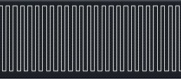
Modulation works by combining a clock frequency (in the case of infra-red this is normally around 38KHz – 40 KHz) with a digital signal. When the digital signal is supposed to be at logic 1 then the clock signal is output rather than a stable logic level 1. When the signal is at logic level 0 then no signal is generated. The following illustrates this:

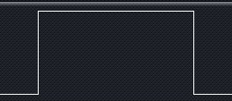
Digital signal:

Digital Signal

Digital Signal

Clock signal:

38.4KHz Clock Signal

38.4KHz Clock Signal

Combined output:

Digital Signal And Clock

Digital Signal And Clock

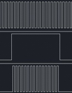
In the final image above, the top trace shows the clock signal, the middle trace shows the digital signal we wish to generate and the lower trace shows the signal which should be output by the circuit.

Hardware Changes

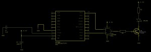
The hardware solution requires the combination of a digital signal with a PWM signal. The easiest way to do this is to use a single AND gate taking input from the digital output required and a clock signal.

Nikon Remote Circuit With Added Modulation

Nikon Remote Circuit With Added Modulation

Searching the RS Components web site lead to a single and gate component for a small price. This would be ideal for solving this problem.

Software Changes

The software changes are minimal as we simply need to configure a timer and turning it on and off as required. We will be using Timer 1, Channel 4 configured to generate a 38.4KHz PWM signal.

Setup

A 38.4KHz signal has a peak to peak duration of 26uS The system is running at 2MHz and so we would need a count value of 52 clock pulses (with no prescalar applied). Using Timer 2, Channel 4 results in the following setup code:

//--------------------------------------------------------------------------------
//
//  Set up Timer 1, channel 4 to output a single pulse lasting 240 uS.
//
void SetupTimer1()
{
    TIM1_ARRH = 0x00;       //  Reload counter = 51
    TIM1_ARRL = 0x33;
    TIM1_PSCRH = 0;         //  Prescalar = 0 (i.e. 1)
    TIM1_PSCRL = 0;
    //
    //  Now configure Timer 1, channel 4.
    //
    TIM1_CCMR4_OC4M = 7;    //  Set up to use PWM mode 2.
    TIM1_CCER2_CC4E = 1;    //  Output is enabled.
    TIM1_CCER2_CC4P = 0;    //  Active is defined as high.
    TIM1_CCR4H = 0x00;      //  26 = 50% duty cycle (based on TIM1_ARR).
    TIM1_CCR4L = 0x1a;
    TIM1_BKR_MOE = 1;       //  Enable the main output.
}

Timer 2 Interrupt Handler

A minor change to the Timer 2 interrupt handler is required to turn off Timer 1 when the signal is no longer being generated:

//--------------------------------------------------------------------------------
//
//  Timer 2 Overflow handler.
//
#pragma vector = TIM2_OVR_UIF_vector
__interrupt void TIM2_UPD_OVF_IRQHandler(void)
{
    _currentPulse++;
    if (_currentPulse == _numberOfPulses)
    {
        //
        //  We have processed the pulse data so stop now.
        //
        PD_ODR_ODR3 = 0;
        TIM2_CR1_CEN = 0;
        TIM1_CR1_CEN = 0;           //  Stop Timer 1.
    }
    else
    {
        TIM2_ARRH = _counterHighBytes[_currentPulse];
        TIM2_ARRL = _counterLowBytes[_currentPulse];
        PD_ODR_ODR3 = _outputValue[_currentPulse];
        TIM2_CR1_URS = 1;
        TIM2_EGR_UG = 1;
    }
    TIM2_SR1_UIF = 0;               //  Reset the interrupt otherwise it will fire again straight away.
}

Main Loop

The final change is to the main program loop. This needs to start Timer 1 when the application starts to output data:

//--------------------------------------------------------------------------------
//
//  Main program loop.
//
void main()
{
    unsigned int pulseLength[] = { 2000U, 27830U, 400U, 1580U, 400U, 3580U, 400U };
    unsigned char onOrOff[] =    {   1,      0,     1,     0,    1,     0,    1 };
    PrepareCounterData(pulseLength, onOrOff, 7);
    __disable_interrupt();
    SetupTimer2();
    SetupTimer1();
    SetupOutputPorts();
    __enable_interrupt();
    PD_ODR_ODR3 = _outputValue[0];
    //
    //  Now we have everything ready we need to force the Timer 2 counters to
    //  reload and enable Timer 2.
    //
    TIM2_CR1_URS = 1;
    TIM2_EGR_UG = 1;
    TIM2_CR1_CEN = 1;
    TIM1_CR1_CEN = 1;       // Start Timer 1
    while (1)
    {
        __wait_for_interrupt();
    }
}

Conclusion

Connecting the logic analyser to the circuit will allow the examination of the three signals, namely, the digital signal required (centre trace), the clock (upper trace) and the modulated output (lower trace):

Modulated IR Signal

Modulated IR Signal

The solid white blocks in the clock and modulated traces show a high density of signals. Zooming in on the right hand side of the capture shows the following:

Modulated IR Signal Zoom View

Modulated IR Signal Zoom View

As you can see, the modulated output is composed of a series of 38.4KHz clock pulses which are only generated when the digital signal should be high (logic 1). The remainder of the time the trace shows no output.

The final test is to see if this will trigger the camera, and yes, it still does.

Nikon D70 Infra-red Control

Saturday, September 7th, 2013

A few weeks ago I started to investigate infra-red transmitters with the intention of looking at implementing a remote control for my DSLR. The first post established the fundamentals by creating a low power transmitter and a receiver. This post takes this one step further and attempts to trigger the Nikon D70 DSLR under the control of a microcontroller.

Background

The Nikon D70 uses the ML-L3 infra-red remote control to trigger the camera. I chose this experiment as a first step to a more advanced remote control for my camera. The experiment builds upon the previous work with the STM8S and infra-red signals to trigger the DSLR.

The remote sequence required to trigger the Nikon D70 has been investigated before. I found the post by Michelle Bighignoli to be the most helpful for this particular exercise.

According to Michelle’s web site, the sequence of pulses required to trigger the camera is as follows:

  • High pulse for 2000uS
  • Low for 27830uS
  • High for 400uS
  • Low for 1580us
  • High for 400uS
  • Low for 3580uS
  • High for 400uS

The pulse is also modulated at a frequency of 38.4KHz.

Hardware

The hardware setup is going to be relatively simple. A basic STM8S circuit is connected to the IR Transmitter circuit using port D3 on the STM8S:
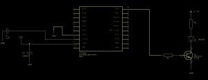
Nikon Infra-red Control Circuit

Nikon Infra-red Control Circuit

You can find out more information about both of these circuits by having a look at the following posts:

All that needs to be done is to put this together on breadboard and setup the STM8S ready for programming.

Software

The initial version of the software will simply emit the infra-red pulse sequence as soon as it powers up as I am only looking at a proof of concept at this stage. We will not consider the topic of modulation at this stage.

Looking at the pulse sequence, the application will need to be able to generate infra-red pulses with control down to the micro-second level. The pulse widths are reasonably large, the smallest is 400uS. Taking this into consideration, the default clock speed of 2MHz will be used for the initial version of the application.

The most obvious way of controlling the pulse widths is to use one of the built in system timers. The most obvious choice is to use Timer 2 as we are going to be using the default clock speed and only require an accuracy of a micro-second or so. This will give a count in the range 0-65535 implying that the maximum pulse width will be 65,535uS assuming we use a prescalar of 2 to divide down the clock frequency used by Timer 2 to 1MHz.

The timers use two eight bit values to control the counting. This will require that the 16-bit values we have for the pulse durations will need to be broken down into two parts either before the sequence starts or as the sequence is being generated (i.e. in the timer Interrupt Service Routine (ISR)). The method chosen here is to perform this operation before the first pulse is generated. This will allow for a quicker ISR.

Design decisions over, let’s start to look at the code.

Pulse and Timer Data

The data for the timers will be broken down into the high and low byte values for the pulse duration. Along with this we will need to store the pulse type, namely high or low.

The pulse data is stored as a sequence of on/off values along with a duration in microseconds:

unsigned int pulseLength[] = { 2000U, 27830U, 400U, 1580U, 400U, 3580U, 400U };
unsigned char onOrOff[] =    {   1,      0,     1,     0,    1,     0,    1 };

This makes the pulse sequence more readable for the programmer. This data needs to be stored as a sequence of 8-bit values representing the high and low bytes of the pulse durations to speed up the ISR.

//
//  Data ready for the pulse timer ISR's to use.
//
unsigned char *_counterHighBytes = NULL;
unsigned char *_counterLowBytes = NULL;
unsigned char *_outputValue = NULL;
int _numberOfPulses = 0;
int _currentPulse = 0;

And to encode the data we need a small helper method:

//--------------------------------------------------------------------------------
//
//  Prepare the data for the timer ISRs.
//
void PrepareCounterData(unsigned int *pulseDuration, unsigned char *pulseValue, unsigned int numberOfPulses)
{
    _numberOfPulses = numberOfPulses;
    if (_counterHighBytes != NULL)
    {
        free(_counterHighBytes);
        free(_counterLowBytes);
        free(_outputValue);
    }
    _counterHighBytes = (unsigned char *) malloc(numberOfPulses);
    _counterLowBytes = (unsigned char *) malloc(numberOfPulses);
    _outputValue = (unsigned char *) malloc(numberOfPulses);
    for (int index = 0; index < numberOfPulses; index++)
    {
        _counterLowBytes[index] = (unsigned char) (pulseDuration[index] & 0xff);
        _counterHighBytes[index] = (unsigned char) (((pulseDuration[index] & 0xff00) >> 8) & 0xff);
        _outputValue[index] = pulseValue[index];
    }
    _currentPulse = 0;
}

Now we have a method of converting the pulses into a format ready for the Timer and the ISR we need to setup the Timer and implement the ISR.

Timer Setup and ISR

Setup is simple as we just need to load the timer values for the first pulse, load the prescalar and enable the interrupts:

//--------------------------------------------------------------------------------
//
//  Setup Timer 2 ready to process the pulse data.
//
void SetupTimer2()
{
    TIM2_ARRH = _counterHighBytes[0];
    TIM2_ARRL = _counterLowBytes[0];
    TIM2_PSCR = _prescalar;
    TIM2_IER_UIE = 1;       //  Enable the update interrupts.
}

The ISR is relatively simple, we need to work out if there is any more pulse data to process. If there is then we load the new data into the counter, set the pulse output and exit the ISR. If there is no more data then we simply set the pulse output and disable the timer.

//--------------------------------------------------------------------------------
//
//  Timer 2 Overflow handler.
//
#pragma vector = TIM2_OVR_UIF_vector
__interrupt void TIM2_UPD_OVF_IRQHandler(void)
{
    _currentPulse++;
    if (_currentPulse == _numberOfPulses)
    {
        //
        //  We have processed the pulse data so stop now.
        //
        PD_ODR_ODR3 = 0;
        TIM2_CR1_CEN = 0;
    }
    else
    {
        TIM2_ARRH = _counterHighBytes[_currentPulse];
        TIM2_ARRL = _counterLowBytes[_currentPulse];
        PD_ODR_ODR3 = _outputValue[_currentPulse];
        TIM2_CR1_URS = 1;
        TIM2_EGR_UG = 1;
    }
    TIM2_SR1_UIF = 0;               //  Reset the interrupt otherwise it will fire again straight away.
}

Output Port

As noted, the application is using Port D3 to output the signal. A small method is required to setup the port accordingly:

//--------------------------------------------------------------------------------
//
//  Now set up the output ports.
//
//  PD3 - IR Pulse signal.
//
void SetupOutputPorts()
{
    PD_ODR = 0;             //  All pins are turned off.
    //
    //  PD4 is the output for the IR control.
    //
    PD_DDR_DDR3 = 1;
    PD_CR1_C13 = 1;
    PD_CR2_C23 = 1;
}

Main program Loop

The main program loop merely sets the stage by initialising the data, output port and timer before wiating for wny interrupts:

//--------------------------------------------------------------------------------
//
//  Main program loop.
//
void main()
{
    unsigned int pulseLength[] = { 2000U, 27830U, 400U, 1580U, 400U, 3580U, 400U };
    unsigned char onOrOff[] =    {   1,      0,     1,     0,    1,     0,    1 };
    PrepareCounterData(pulseLength, onOrOff, 7);
    __disable_interrupt();
    SetupTimer2();
    SetupOutputPorts();
    __enable_interrupt();
    PD_ODR_ODR3 = _outputValue[0];
    //
    //  Now we have everything ready we need to force the Timer 2 counters to
    //  reload and enable Timer 2.
    //
    TIM2_CR1_URS = 1;
    TIM2_EGR_UG = 1;
    TIM2_CR1_CEN = 1;
    while (1)
    {
        __wait_for_interrupt();
    }
}

Conclusion

Putting this all together and wiring up the oscilloscope we find the following generated when the circuit is turned on:

Output From Nikon Infra-red Control Circuit

Output From Nikon Infra-red Control Circuit

Examination of the timings of the pulses reveals that the pulse widths match those in the original specification above. The small spike at the start of the pulse sequence only appears when the circuit is first turned on.

At the moment we are only generating the raw pulses, we have not started to modulate the signal using the 38.4KHz carrier. This is left for a future experiment or indeed as a exercise for the reader.

One thing I could not resist was trying this with the Nikon camera, even though the specification stated that a 38.4KHz carrier was required. Running the code with the camera set to manual mode resulted in the camera being triggered.

So some future work:

  • Add the modulation
  • Increase the power of the infra-red output