At some point in the development lifecycle we will hit some unexpected application behaviour. At this point we reach for the debugger to allow us to connect to the application an interrogate the state and hopefully we will be able to determine the cause of the problem. Working with NuttX is no different from any other application. The only complication we have is connecting to application running on the PicoW requires a debug adapter. Luckily, the Raspberry Pi Foundation has an affordable solution to this problem.
Environment
The getting started guide for the Pico has instructions on how to set up the environment for Linux, Mac and Windows. This post will be following the guide for MacOS adding some hardware to allow for a stable connection between the debug probe and the PicoW.
There are two options for the debug probe:
- The Raspberry Pi debug probe
- Use a Pico programmed as a debug probe
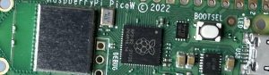
I have a number of Pico and PicoW boards and so the later option, using a Pico programmed as a debug probe, is going to be the most cost effective and this is the route we will look at here.
Hardware
For the purpose of discussion we will use the following terms to describe the two boards:
- Picoprobe – Pico that is programmed to be a debug probe
- Target – PicoW that is running the application we wish to debug
The getting stared guide shows how two Pico boards should be connected to provide both debugging and serial console output through a UART on the target board. This shows the two boards on a breadboard setup (image is taken from the Raspberry Pi Pico getting started guide under CC-BY-ND license).
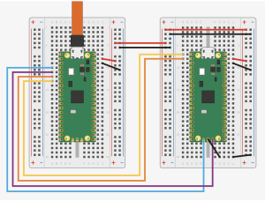
Picoprobe and Pico Fritzing
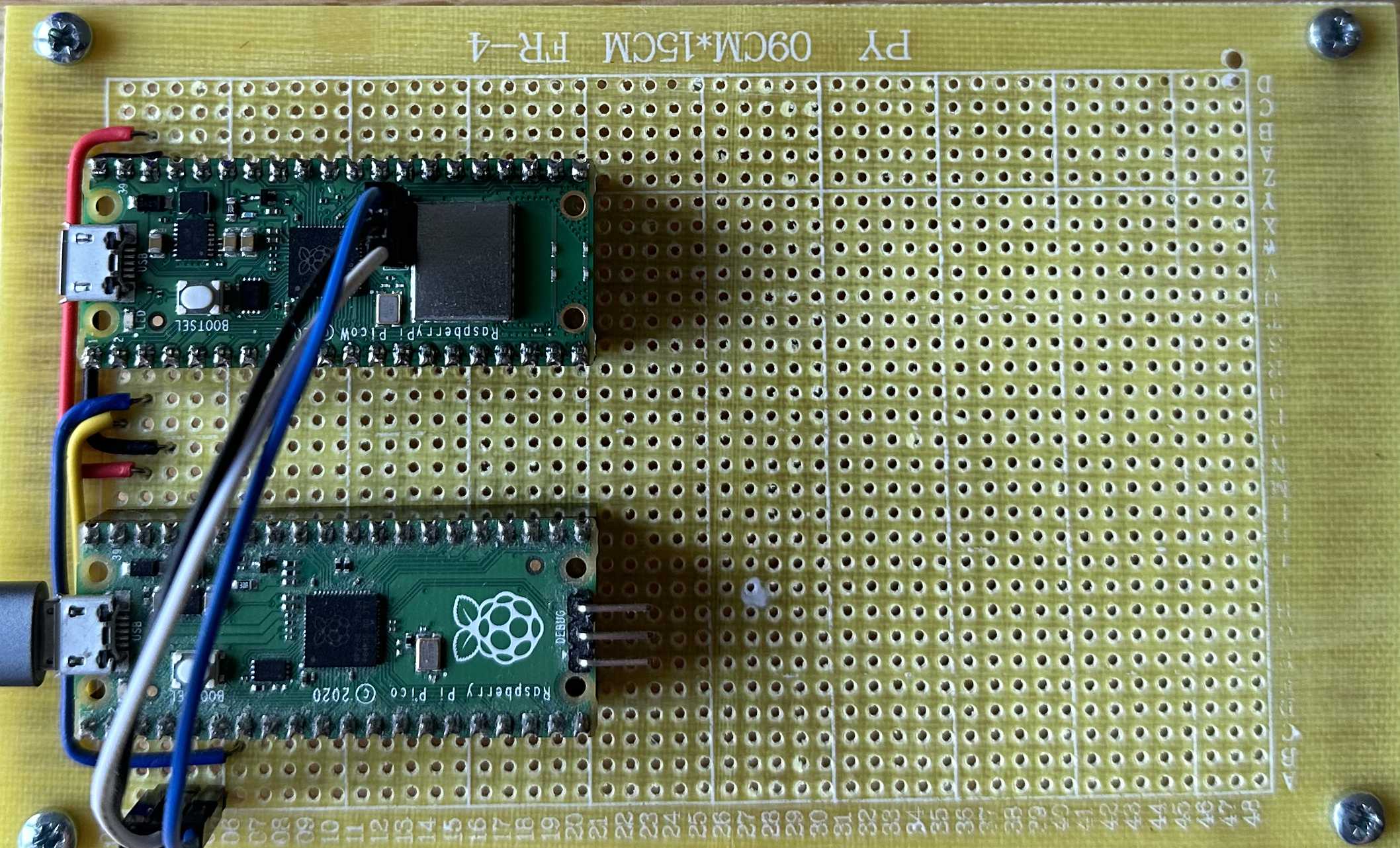
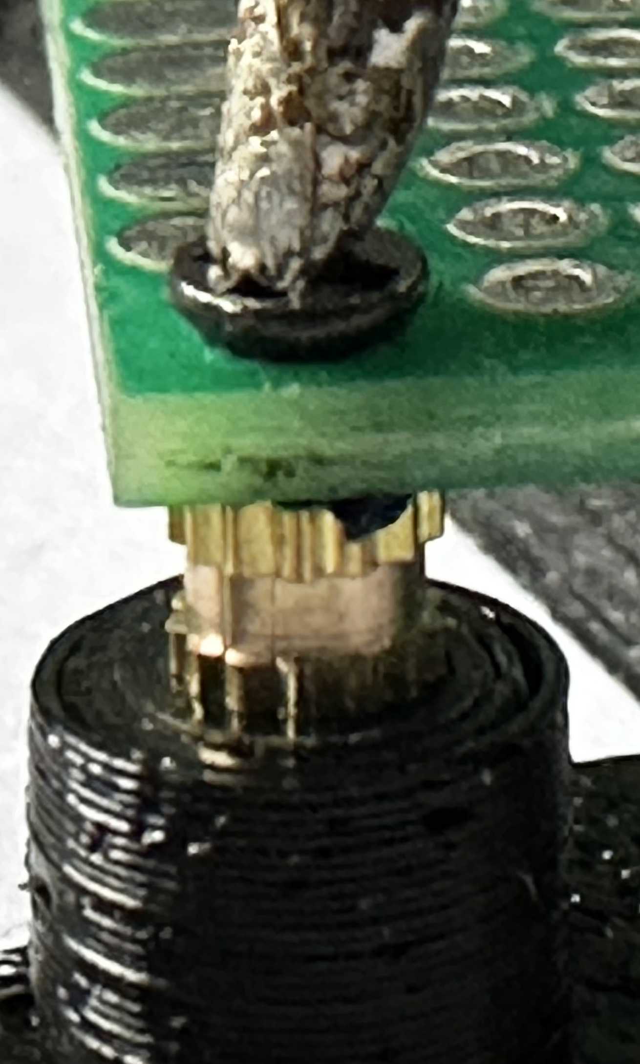
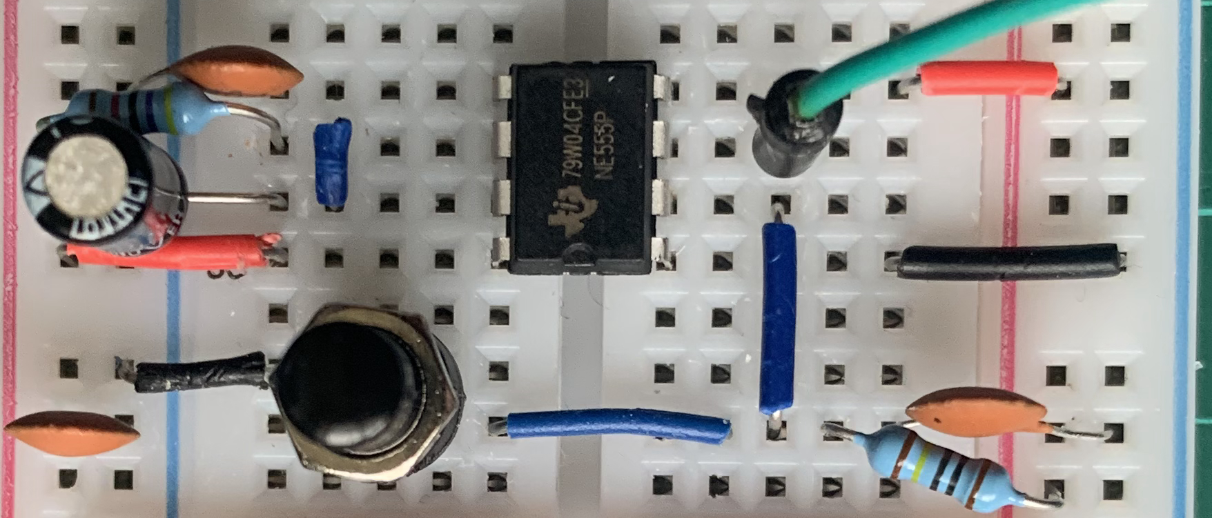
The same setup can be reproduced on protoboard. This will make the setup a little more robust and permanent. Breaking out the soldering iron and the parts bin yielded the following:
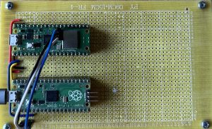
Pico on Protoboard
The flying leads are needed to connect to the SWD debug headers on the PicoW as it was not possible to connect these through to the protoboard. The black (GND) and red (5V) wires provide power to the target board. This means that we only have one connector to the system, namely to the Picoprobe but we must take care not to exceed the power capabilities of the USB connection.
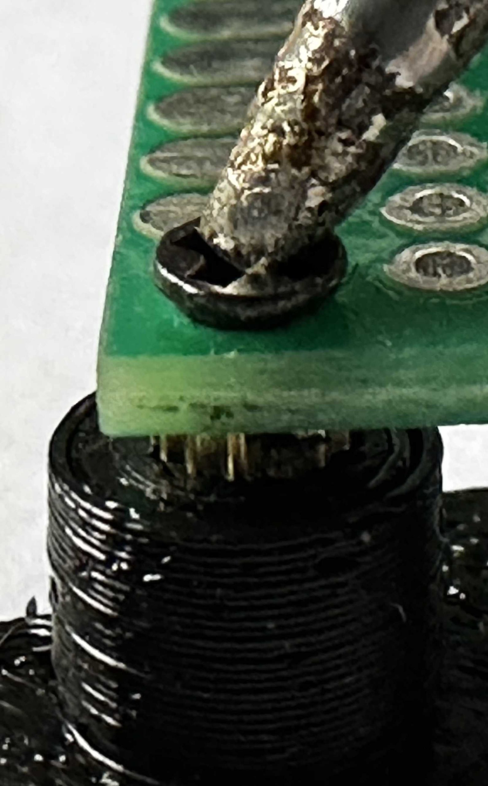
The white (SWCLK) and blue (SWDIO) flying leads provide the debug connection between the two boards. As with the permanent connections above, the black lead is a GND connection.
The blue and yellow leads connected permanently to the protoboard connect the UART from the target board through to the picoprobe. The picoprobe will use the USB connection to present the host computer with a connection through to the UART on the target board.
Software
The first piece of software needed is the Picoprobe software itself. There are instruction on how to build this but I found the simplest thing to do was to download the latest release from the Picoprobe GitHub repository. At the time of writing this is version 1.0.2. The Picoprobe software is deployed to the Pico being used as a Picoprobe in the usual way, reset the Pico whilst hold the BootSel button and then drag and drop the firmware file onto the drive present to the host computer.
The next thing we need is a version of openocd that can talk to the Picoprobe. The machine I am using is used to develop software for multiple boards and so the preferable solution is to build the Raspberry Pi Pico version of openocd for this setup and then reference this locally rather than install the software globally. This is the same approach taken for the various development environment I use to prevent them interfering with each other.
Following the guide (for Mac) we need to execute the following commands:
cd ~/pico
git clone https://github.com/raspberrypi/openocd.git --branch picoprobe --depth=1 $ cd openocd
export PATH="/usr/local/opt/texinfo/bin:$PATH" 1
./bootstrap
./configure --enable-picoprobe --disable-werror 2
make -j4
Check the latest version of the guide for instructions for your OS.
Now to try openocd… This is where I hit a problem caused by having out of date documentation. Following the latest documentation we need to execute the following command:
src/openocd -f interface/cmsis-dap.cfg -f target/rp2040.cfg -c "adapter speed 5000" -s tcl
I was following I hit two errors due to the out of date documentation:
- Error: Can’t find a picoprobe device! Please check device connections and permissions.
- Error: CMSIS-DAP command CMD_DAP_SWJ_CLOCK failed.
Both of these errors were corrected by using the command above to connect to the debug probe. Moral of the story, make sure you are using the latest information. If everything goes well then we should be rewarded with something similar to the following output:
Open On-Chip Debugger 0.11.0-g4f2ae61 (2023-06-10-18:20)
Licensed under GNU GPL v2
For bug reports, read
	http://openocd.org/doc/doxygen/bugs.html
Info : auto-selecting first available session transport "swd". To override use 'transport select <transport>'.
Info : Hardware thread awareness created
Info : Hardware thread awareness created
Info : RP2040 Flash Bank Command
adapter speed: 5000 kHz

Info : Listening on port 6666 for tcl connections
Info : Listening on port 4444 for telnet connections
Info : Using CMSIS-DAPv2 interface with VID:PID=0x2e8a:0x000c, serial=E66058388356A232
Info : CMSIS-DAP: SWD  Supported
Info : CMSIS-DAP: FW Version = 2.0.0
Info : CMSIS-DAP: Interface Initialised (SWD)
Info : SWCLK/TCK = 0 SWDIO/TMS = 0 TDI = 0 TDO = 0 nTRST = 0 nRESET = 0
Info : CMSIS-DAP: Interface ready
Info : clock speed 5000 kHz
Info : SWD DPIDR 0x0bc12477
Info : SWD DLPIDR 0x00000001
Info : SWD DPIDR 0x0bc12477
Info : SWD DLPIDR 0x10000001
Info : rp2040.core0: hardware has 4 breakpoints, 2 watchpoints
Info : rp2040.core1: hardware has 4 breakpoints, 2 watchpoints
Info : starting gdb server for rp2040.core0 on 3333
Info : Listening on port 3333 for gdb connections
If we have got here then we have the the debug probe programmed and we have a copy of openocd that can communicate with the picoprobe.
Reconfiguring NuttX
In previous posts we used UART over USB to communicate with the host computer. The picoprobe gives us another option, using the UART on the target board which is routed through the picoprobe. We must reconfigure NuttX in order to take advantage of the UART redirection. The configuration we want is raspberrypi-pico-w:nsh, so following the first post in this series and making the change to the configuration we need to execute the following:
make distclean
./tools/configure.sh -l raspberrypi-PicoW:nsh
make -j
At the end of this process we should have a new nuttx.uf2 file configured to use the UART port on the target board to communicate with the NuttX shell. This UF2 file can be deployed using the usual deployment process (Bootsel and reset followed by drag and dropping the file) to the target board.
At this point we should have two Pico boards programmed, one to be the picoprobe and one to be the target board (with NuttX). Now we can connect the boards (in my case using the protoboard shown above) and verify that NuttX is active and communicating through the UART.
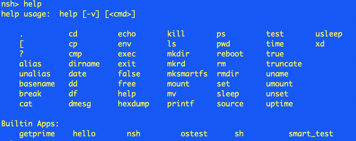
Plugging the Pico (picoprobe) and the PicoW (target board) into the protoboard and then connecting the host computer to the picoprobe through USB presents the computer with a new serial port, usbmodem14302. Connecting to this port and hitting enter shows the nsh prompt. Asking for help shows the expected output.
nsh> help
help usage:  help [-v] [<cmd>]

    .         cat       df        free      mount     rmdir     truncate
    [         cd        dmesg     help      mv        set       uname
    ?         cp        echo      hexdump   printf    sleep     umount
    alias     cmp       env       kill      ps        source    unset
    unalias   dirname   exec      ls        pwd       test      uptime
    basename  date      exit      mkdir     reboot    time      usleep
    break     dd        false     mkrd      rm        true      xd

Builtin Apps:
    nsh  sh
nsh>
So we have a good UART connection and openocd can connect to the picoprobe.
Now we need to connect the debugger to openocd.
Debugging
To debug the board we will start with GDB, specifically arm-none-eabi-gdb-py as this has Python scripting enabled. We can use the scripting engine to automate some tasks later.
First thing to do is add a .gdbinit file to the directory we will be executing GDB from, in this case we will use the nuttx directory. The following commands should setup GDB and openocd ready for debugging. The nuttx ELF file will be loaded for us so by the time the GDB prompt is show we will have the symbol file loaded. Our .gdbinit file should look something like this:
set history save on
set history size unlimited
set history remove-duplicates unlimited
set history filename ~/.gdb_history

set output-radix 16
set mem inaccessible-by-default off

set remote hardware-breakpoint-limit 4
set remote hardware-watchpoint-limit 2

set confirm off

file nuttx
add-symbol-file -readnow nuttx

target extended-remote :3333
mon gdb_breakpoint_override hard
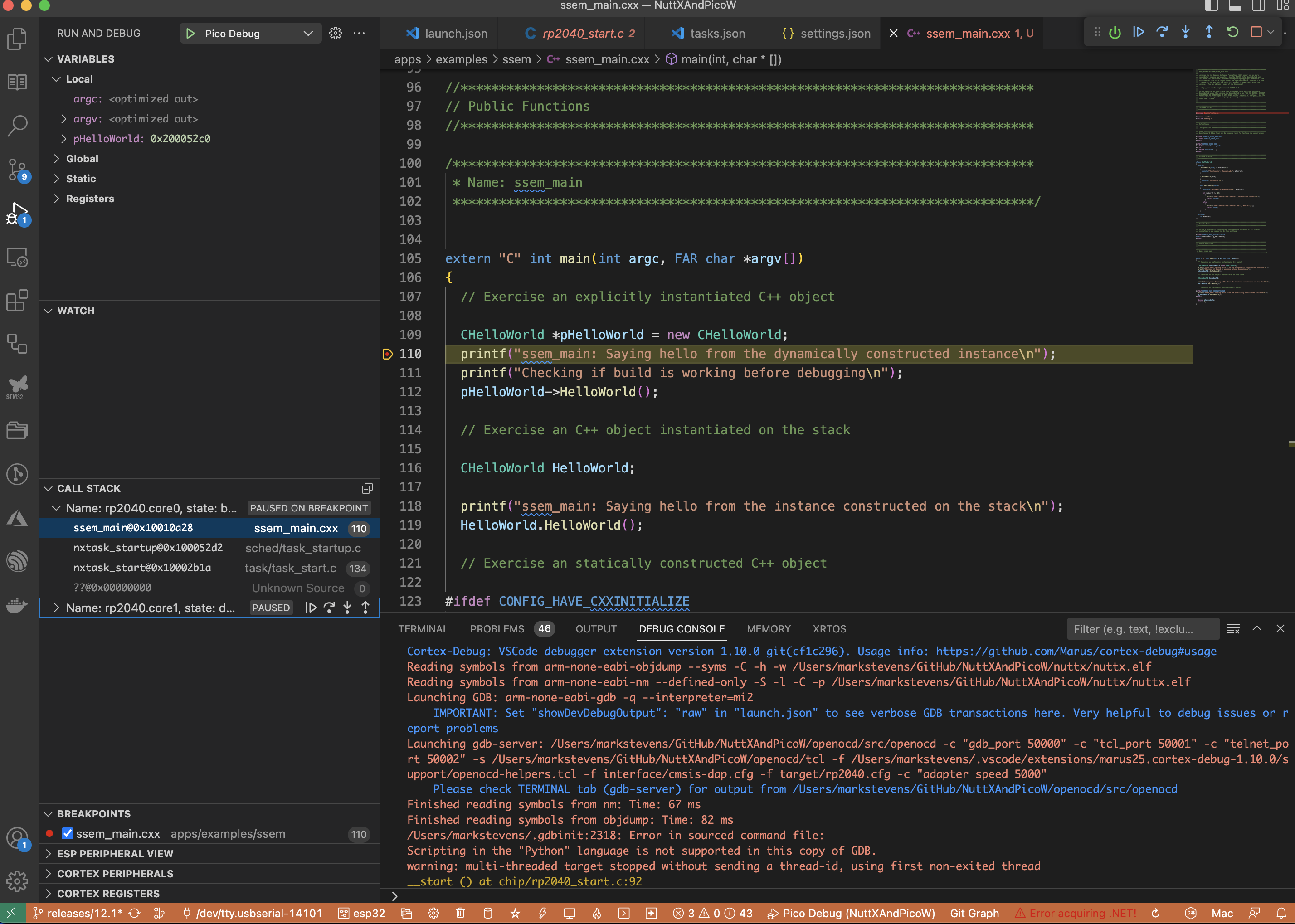
To debug we will need two terminal sessions open. In the first session run openocd as described above. In the second session start GDB (simply enter the command arm-none-eabi-gdb-py in the terminal session) making sure that you are in the directory containing the nuttx file and the .gdbinit file. If you are successful then you will see something like this:
GNU gdb (GDB) 13.1
Copyright (C) 2023 Free Software Foundation, Inc.
License GPLv3+: GNU GPL version 3 or later <http://gnu.org/licenses/gpl.html>
This is free software: you are free to change and redistribute it.
There is NO WARRANTY, to the extent permitted by law.
Type "show copying" and "show warranty" for details.
This GDB was configured as "x86_64-apple-darwin22.3.0".
Type "show configuration" for configuration details.
For bug reporting instructions, please see:
<https://www.gnu.org/software/gdb/bugs/>.
Find the GDB manual and other documentation resources online at:
    <http://www.gnu.org/software/gdb/documentation/>.

For help, type "help".
Type "apropos word" to search for commands related to "word".
add symbol table from file "../nuttx/nuttx"
We can now start to debug the application on the board. A few simple tests, firstly, reset the board with the GDB command mon reset halt. We should see something like this:
target halted due to debug-request, current mode: Thread
xPSR: 0xf1000000 pc: 0x000000ea msp: 0x20041f00
target halted due to debug-request, current mode: Thread
xPSR: 0xf1000000 pc: 0x000000ea msp: 0x20041f00
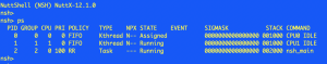
We can now set a breakpoint, say in nsh_main (b nsh_main) and run the application to the breakpoint (c). If we then ask for information about the threads (info thre) we should see something like this:
  Id   Target Id                                           Frame
* 1    Thread 1 (Name: rp2040.core0, state: breakpoint)    nsh_main (argc=0x1, argv=0x20003170) at nsh_main.c:58
  2    Thread 2 (Name: rp2040.core1, state: debug-request) 0x000000ea in ?? ()
Conclusion
Getting debugging up and running took a little more effort than I expected but was not expensive due to the ability to use a Pico to debug a Pico. There is some excellent debugger documentation on the NuttX web site. This suggests that openocd should support NuttX however I was not able to get this working with the Raspberry Pi release of openocd. It was a question of having Pico support or NuttX support. I’m going with the Pico support for the minute.
I was hoping to use the picoprobe board to deploy the application meaning that we only have one connection between the host computer and the development hardware. A little more research is going to be necessary to see if this can be done.