Transmitting Data Using the STM8S SPI Master Mode
Sunday, June 23rd, 2013So far in The Way of the Register series we have only looked at SPI from a slave device point of view as we have been working towards creating a Netduino GO! module. For every slave device there must be a master, here we will look at configuring the STM8S to operate in SPI master mode.
The project will look at controlling a TLC5940 in order to emulate the work described in the post TLC5940 16 Channel PWM Driver. We could simply bit-bang the data out to the chip but instead we will use the SPI interface to achieve this.
The project breaks down into the following steps:
- Generate the grey scale clock and blank signals
- Bit-Bang data out over GPIO pins to create an operational circuit
- Convert the data transmission to SPI
See the quoted post for a description of how this chip works and for an explanation of the terminology used.
Generating the Grey Scale Clock and Blank Signals
The TLC5940 generated 4,096 grey scale values by using a PWM counter. Once the counter reaches 4096 pulses it stops until it is told to restart. The Blank pulse acts as a restart signal. This project will be controlling LEDs and so will want to continuously keep the counter running. If we did not keep the counter in the TLC5940 running then the LEDs would light for a short while and then simply turn off and remain off.
The greyscale clock is generated by using the Configurable Clock Output (CCO) pin on the STM8S. This pin simply outputs the clock pulses used to drive the STM8S. Reviewing the data sheet we find that the maximum value for the grey scale clock is 30MHz. Using out standard clock initialisation generates a clock with a frequency of 16MHz (approximately). This is well within the tolerances of the TLC5940. To output this we need to make a simple modification to our standard code, name change the line:
CLK_CCOR = 0; // Turn off CCO.
to:
CLK_CCOR = 1; // Turn on CCO.
The starting point for our application becomes:
#if defined DISCOVERY
    #include <iostm8S105c6.h>
#elif defined PROTOMODULE
    #include <iostm8s103k3.h>
#else
    #include <iostm8s103f3.h>
#endif
#include <intrinsics.h>

//
//  Setup the system clock to run at 16MHz using the internal oscillator.
//
void InitialiseSystemClock()
{
    CLK_ICKR = 0;                       //  Reset the Internal Clock Register.
    CLK_ICKR_HSIEN = 1;                 //  Enable the HSI.
    CLK_ECKR = 0;                       //  Disable the external clock.
    while (CLK_ICKR_HSIRDY == 0);       //  Wait for the HSI to be ready for use.
    CLK_CKDIVR = 0;                     //  Ensure the clocks are running at full speed.
    CLK_PCKENR1 = 0xff;                 //  Enable all peripheral clocks.
    CLK_PCKENR2 = 0xff;                 //  Ditto.
    CLK_CCOR = 1;                       //  Turn on CCO.
    CLK_HSITRIMR = 0;                   //  Turn off any HSIU trimming.
    CLK_SWIMCCR = 0;                    //  Set SWIM to run at clock / 2.
    CLK_SWR = 0xe1;                     //  Use HSI as the clock source.
    CLK_SWCR = 0;                       //  Reset the clock switch control register.
    CLK_SWCR_SWEN = 1;                  //  Enable switching.
    while (CLK_SWCR_SWBSY != 0);        //  Pause while the clock switch is busy.
}

//
//  Main program loop.
//
void main()
{
    //
    //  Initialise the system.
    //
    __disable_interrupt();
    InitialiseSystemClock();
    __enable_interrupt();
    while (1)
    {
        __wait_for_interrupt();
    }
}
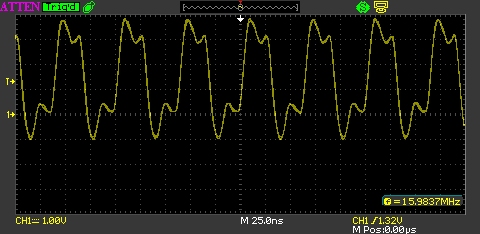
Wiring up the STM8S and connecting the scope to PC4 (CCO output pin) gives the following trace on the scope:
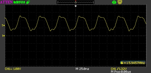
CCO On Scope
The trace on the scope has a minimum value of around 680mV and a maximum of 2.48V. In an ideal world this signal should range from 0 to 3.3V (based upon a 3.3V supply). Adding an inverter from a 74HC04 and feeding the signal through one of the gates gives the following trace:
Inverter output on the scope
This is starting to look a lot better. The next task is to create the Blank signal. There are several ways of doing this. The most automatic way of doing this is to generate a very short PWM pulse using one of the timers in the STM8S. One drawback of this method is that it is more difficult to generate a Blank pulse on demand. Instead we will use the interrupt method described in the same article. Whilst not automatic it is still a trivial task to complete. We simply modify the code from the method to load the counters with 4,096. The code for the GPIO port, timer and interrupt becomes:
//
//  Timer 2 Overflow handler.
//
#pragma vector = TIM2_OVR_UIF_vector
__interrupt void TIM2_UPD_OVF_IRQHandler(void)
{
    PD_ODR_ODR4 = 1;
    PD_ODR_ODR4 = 0;
    TIM2_SR1_UIF = 0;       //  Reset the interrupt otherwise it will fire again straight away.
}

//
//  Setup Timer 2 to generate an interrupt every 4096 clock ticks.
//
void SetupTimer2()
{
    TIM2_PSCR = 0x00;       //  Prescaler = 1.
    TIM2_ARRH = 0x10;       //  High byte of 4096.
    TIM2_ARRL = 0x00;       //  Low byte of 4096.
    TIM2_IER_UIE = 1;       //  Turn on the interrupts.
    TIM2_CR1_CEN = 1;       //  Finally enable the timer.
}

//
//  Setup the output ports used to control the TLC5940.
//
void SetupOutputPorts()
{
    PD_ODR = 0;             //  All pins are turned off.
    PD_DDR_DDR4 = 1;        //  Port D, pin 4 is used for the Blank signal.
    PD_CR1_C14 = 1;         //  Port D, pin 4 is Push-Pull
    PD_CR2_C24 = 1;         //  Port D, Pin 4 is generating a pulse under 2 MHz.
}
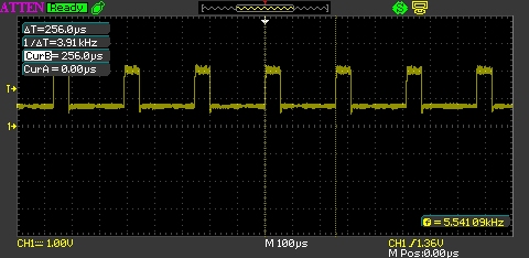
Hooking up the scope to PD4 gives the following trace:
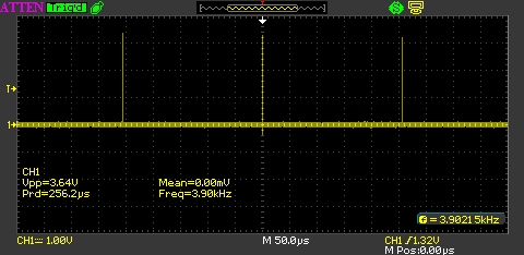
Blanking pulses
The single pulses are being generated at a frequency of approximately 3.9kHz. A little mental arithmetic dividing the 16MHz clock by 4,096 comes out to about 3,900.
Zooming in on the signal we see:
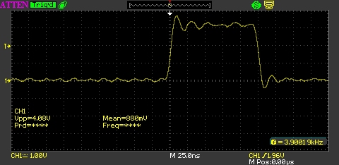
Single Blanking Pulse
This shows that the signal is 125nS wide. This is acceptable as the minimum pulse width given in the data sheet is 20nS.
So at this point we have the 16MHz grey scale clock signal and the Blank pulse being generated every 4,096 clock pulses.
Connecting the TLC5940
The next task is to connect the STM8S to the TLC5940. You should refer to the article TLC5940 16 Channel PWM Driver for more information on the pins and their meaning. For this exercise we will use the following mapping:
| STM8S Pin | TLC5940 Pin |
| PD4 | Blank (pin 23) |
| PD3 | XLAT (pin 24) |
| PD2 | VPRG (pin 27) |
| PD5 | Serial data (pin 26) |
| PD6 | Serial clock (pin 25) |
| PC4 (via inverter) | GSCLK (pin 18) |
You will note that the serial data and clock are currently connected to PD5 and PD6 respectively. Whilst the eventual aim is to communicate with the TLC5940 via SPI, the initial communication will be using Bit-Banging. We will move on to using SPI once the operation of the circuit has been proven using tested technology.
The first changes we will have to make create some #define statements to make the code a little more readable. We also add some storage space for the grey scale and dot correction data.
//
//  Define which pins on Port D will be used as control signals for the TLC5940.
//
//  BLANK - A pulse from low to high causes the TLC5940 to restart the counter
//  XLAT - A high pulse causes the data to be transferred into the DC or GS registers.
//  VPRG - Determines which registers are being programmed, High = DC, Low = GS.
//
#define PIN_BLANK                   PD_ODR_ODR4
#define PIN_XLAT                    PD_ODR_ODR3
#define PIN_VPRG                    PD_ODR_ODR2
//
//  Bit bang pins.
//
#define PIN_BB_DATA                 PD_ODR_ODR5
#define PIN_BB_CLK                  PD_ODR_ODR6
//
//  Values representing the modes for the VPRG pin.
//
#define PROGRAMME_DC                1
#define PROGRAMME_GS                0

//
//  TLC5940 related definitions.
//
#define TLC_NUMBER                  1
#define TLC_DC_BYTES_PER_CHIP       12
#define TLC_DC_BYTES                TLC_NUMBER * TLC_DC_BYTES_PER_CHIP
#define TLC_GS_BYTES_PER_CHIP       24
#define TLC_GS_BYTES                TLC_NUMBER * TLC_GS_BYTES_PER_CHIP

//
//  Next we need somewhere to hold the data.
//
unsigned char _greyScaleData[TLC_GS_BYTES];
unsigned char _dotCorrectionData[TLC_DC_BYTES];
The Bit-Banging methods should look familiar to anyone who has been reading any of the posts in The Way of the Register series.
//--------------------------------------------------------------------------------
//
// Bit bang data.
//
// TLC5940 expects the data to be shifted MSB first. The data
// is shifted in on the rising edge of the clock.
//
void BitBang(unsigned char byte)
{
for (short bit = 7; bit >= 0; bit--)
{
if (byte & (1 << bit))
{
PIN_BB_DATA = 1;
}
else
{
PIN_BB_DATA = 0;
}
PIN_BB_CLK = 1;
PIN_BB_CLK = 0;
}
PIN_BB_DATA = 0;
}
//--------------------------------------------------------------------------------
//
// Bit bang a buffer of data.
//
void BitBangBuffer(unsigned char *buffer, int size)
{
for (int index = 0; index < size; index++)
{
BitBang(buffer[index]);
}
}
Related to the Bit-Banging methods are the two methods which will send the grey scale and dot correction data:
//--------------------------------------------------------------------------------
//
//  Send the grey scale data to the TLC5940.
//
void SendGreyScaleData(unsigned char *buffer, int length)
{
    PIN_VPRG = PROGRAMME_GS;
    BitBangBuffer(buffer, length);
    PulseXLAT();
    PulseBlank();
}

//--------------------------------------------------------------------------------
//
//  Send the dot correction buffer to the TLC5940.
//
void SendDotCorrectionData(unsigned char *buffer, int length)
{
    PIN_VPRG = PROGRAMME_DC;
    BitBangBuffer(buffer, length);
    PulseXLAT();
    PulseBlank();
}
We also need a few methods to make the TLC5940 latch the data and also restart the counters:
//--------------------------------------------------------------------------------
//
//  Pulse the Blank pin in order to make the TLC5940 reload the counters and
//  restart timer.
//
void PulseBlank()
{
    PIN_BLANK = 1;
    PIN_BLANK = 0;
}

//--------------------------------------------------------------------------------
//
//  Pulse the XLAT pin in order to make the TLC5940 transfer the
//  data from the latches into the appropriate registers.
//
void PulseXLAT()
{
    PIN_XLAT = 1;
    PIN_XLAT = 0;
}
Next we need to set the initial condition. For this we set the TLC dot correction off and also turn all of the LEDs off:
//--------------------------------------------------------------------------------
//
//  Initialise the TLC5940.
//
void InitialiseTLC5940()
{
    for (int index = 0; index < TLC_DC_BYTES; index++)
    {
        _dotCorrectionData[index] = 0xff;
    }
    for (int index = 0; index < TLC_GS_BYTES; index++)
    {
        _greyScaleData[index] = 0;
    }
    SendDotCorrectionData(_dotCorrectionData, TLC_DC_BYTES);
    SendGreyScaleData(_greyScaleData, TLC_GS_BYTES);
}
The final support method we need to add is the method which sets the brightness of an LED. The brightness is a 12-bit value (0-4095). This means each LED uses 1.5 bytes for the brightness value. The following methods breaks down the value and ensures that the correct bits are set in the grey scale buffer depending upon which LED is being changed:
//--------------------------------------------------------------------------------
//
//  Set the brightness of an LED.
//
void SetLEDBrightness(int ledNumber, unsigned short brightness)
{
    int offset = (ledNumber >> 1) * 3;
    if (ledNumber & 0x01)
    {
        _greyScaleData[offset + 1] = (unsigned char) (_greyScaleData[offset + 1] & 0xf0) | ((brightness & 0x0f00) >> 8);
        _greyScaleData[offset + 2] = (unsigned char) (brightness & 0xff);
    }
    else
    {
        _greyScaleData[offset] = (unsigned char) ((brightness & 0x0ff0) >> 4) & 0xff;
        _greyScaleData[offset + 1] = (unsigned char) ((brightness & 0x0f) >> 4) | (_greyScaleData[offset + 1] & 0x0f);
    }
}
We should also create a similar method for changing the dot correction value for an LED. This is left as an exercise for the reader as we will not be changing this value in this code.
Proving the concept
If we have connected the TLC5940 correctly and our code works we should be able to connect up some LEDs (common anode) to the TLC5940 and change the brightness under program control.
This main program loop slowly increases the brightness of the LEDs. When they are at full brightness they are turned off and the process starts again:
//--------------------------------------------------------------------------------
//
//  Main program loop.
//
void main()
{
    //
    //  Initialise the system.
    //
    __disable_interrupt();
    InitialiseSystemClock();
    SetupOutputPorts();
    SetupTimer2();

    InitialiseTLC5940();
    __enable_interrupt();
    //
    //  Main program loop.
    //
    int brightness = 0;
    int counter = 0;
    while (1)
    {
        __wait_for_interrupt();
        counter++;
        if (counter == 20)
        {
            TIM2_CR1_CEN = 0;
            counter = 0;
            for (int index = 0; index < 16; index++)
            {
                SetLEDBrightness(index, brightness);
            }
            SendGreyScaleData(_greyScaleData, TLC_GS_BYTES);
            brightness++;
            if (brightness == 4096)
            {
                brightness = 0;
            }
            TIM2_CR1_CEN = 1;       //  Finally re-enable the timer.
        }
    }
}
If you connect a scope to the cathode of one of the LEDs you will see that the wave form slowly changes over time. At the start, the LED is fully on and the trace on the scope shows a horizontal line, i.e. a constant voltage. As time moves on and the value in the dot correction buffer changes you start to see a PWM signal similar to the following:
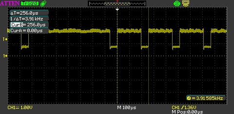
PWM Output On Scope 1
This trace shows the signal when the LEDs are a little brighter:
PWM Output On Scope 2
Having arrived here we now know that the circuit has been connected correctly and that the control logic in the main method works. We can now move on to considering what we need to do in order to use SPI in master mode. The aim will be to simply remove the Bit-Banging methods and replace these with an interrupt driven SPI master algorithm.
SPI Master
So now we have a working circuit we need to look at SPI on the STM8S. Firstly let’s remind ourselves of the serial communication parameters for the TLC5940. This chip reads the data on the leading clock edge (CPHA = 1). We have also set the clock idle state to low (CPOL = 0).
It is also advisable to start off using the lowest clock speed for SPI in order to confirm correct operation of the software and circuit. Lower speed are less likely to be subject to interference.
SPI Registers
You should review the previous articles on SPI communication if you are not already familiar with the SPI registers we have used so far. In this post we will only discuss the new settings required to switch from being a SPI slave device to a SPI master device.
SPI_CR1_BR – Baud Rate Control
The SPI baud rate is determined by the master clock frequency and the value in this register. The divisor used to set the baud rate according to the following table:
| SPI_CR1_BR | Divisor |
| 000 | 2 |
| 001 | 4 |
| 010 | 8 |
| 011 | 16 |
| 100 | 32 |
| 101 | 64 |
| 110 | 128 |
| 111 | 256 |
The SPI baud rate is calculated as fmaster / divisor. So for our master clock speed of 16MHz we get the lowest clock speed of 16,000,000 / 256, or 62,500Hz.
SPI_CR1_MSTR – Master Selection
Setting this bit switches SPI into master mode (see also SPI_CR1_SPE).
Note that the reference for the STM8S also states that this bit (and SPI_CR1_SPE) will only remain set whilst NSS is high. It this therefore essential to connect NSS to Vcc if this device is not being used as a slave device.
Implementing SPI
Using SPI presents us with a small problem, namely the program will have to start to operate in a more asynchronous way. The code presented so far has only one interrupt to be concerned with, namely the timer used to control the Blank signal. Adding SPI to the mix means that we will have to also consider the SPI interrupt as well. It also adds the complication of sending dot correction data followed by grey scale data. This last problem will not be covered here and is left as an exercise for the reader.
The initialisation code merely sets things up for us:
//--------------------------------------------------------------------------------
//
//  Initialise SPI to be SPI master.
//
void SetupSPIAsMaster()
{
    SPI_CR1_SPE = 0;                    //  Disable SPI.
    SPI_CR1_CPOL = 0;                   //  Clock is low when idle.
    SPI_CR1_CPHA = 0;                   //  Capture MSB on first edge.
    SPI_ICR_TXIE = 1;                   //  Enable the SPI TXE interrupt.
    SPI_CR1_BR = 7;                     //  fmaster / 256 (62,500 baud).
    SPI_CR1_MSTR = 1;                   //  Master device.
}
Much of the code should be familiar as it has been used in previous posts discussing SPI slave devices. Not however that we do not enable SPI at this point. We simply set the scene for us to use SPI later.
The SPI data transfers will be controlled by using an interrupt service routine:
//--------------------------------------------------------------------------------
//
//  SPI Interrupt service routine.
//
#pragma vector = SPI_TXE_vector
__interrupt void SPI_IRQHandler(void)
{
    //
    //  Check for an overflow error.
    //
    if (SPI_SR_OVR)
    {
        (void) SPI_DR;                      // These two reads clear the overflow
        (void) SPI_SR;                      // error.
        return;
    }
    if (SPI_SR_TXE)
    {
        //
        //  Check if we have more data to send.
        //
        if (_txBufferIndex == _txBufferSize)
        {
            while (SPI_SR_BSY);
            SPI_CR1_SPE = 0;
            _txBuffer = 0;
            PulseXLAT();
            PulseBlank();
            TIM2_CR1_CEN = 1;
        }
        else
        {
            SPI_DR = _txBuffer[_txBufferIndex++];
        }
    }
}
The main works starts when we have established that the transmit buffer is empty (SPI_SR_TXE is set). If we have more data then we put the byte into the data register (SPI_DR). If we have transmitted all the data we have then we wait for the last byte to complete transmission (SPI_SR_BSY becomes false) before we start to terminate the end of the SPI communication.
In order to send some data we really just need to setup the pointers and counters correctly and then enable SPI. So the SendGreyScaleData method becomes:
//--------------------------------------------------------------------------------
//
//  Send the grey scale data to the TLC5940.
//
void SendGreyScaleData(unsigned char *buffer, int length)
{
    PIN_VPRG = PROGRAMME_GS;
    _txBuffer = buffer;
    _txBufferIndex = 0;
    _txBufferSize = length;
    TIM2_CR1_CEN = 0;
    SPI_CR1_SPE = 1;
}
We also need to have a look at the main program loop as we use the __wait_for_interrupt() method in order to determine when we should start to process the next LED brightness value. We now need to ignore the interrupts when SPI is enabled otherwise the brightness will increase each time the transmit buffer is empty. A crude implementation eliminating the SPI interrupts is:
int brightness = 0;
int counter = 0;
while (1)
{
    __wait_for_interrupt();
    if (!SPI_CR1_SPE)
    {
        counter++;
        if (counter == 20)
        {
            TIM2_CR1_CEN = 0;
            counter = 0;
            for (int index = 0; index < 16; index++)
            {
                SetLEDBrightness(index, brightness);
            }
            SendGreyScaleData(_greyScaleData, TLC_GS_BYTES);
            brightness++;
            if (brightness == 4096)
            {
                brightness = 0;
            }
            TIM2_CR1_CEN = 1;       //  Finally re-enable the timer.
        }
    }
}
Making these changes and running the code shows that the system operated as before.
Increasing the Baud Rate
As noted earlier, the baud rate has been set low in order to reduce the chance of any problems being experienced due to interference. Now we have established that using SPI communication is possible and the circuit works as before we can start to increase the baud rate. Using our 16MHz clock we find we have the following baud rates which are theoretically possible:
| SPI_CR1_BR | Divisor | SPI Frequency |
| 000 | 2 | 8 MHz |
| 001 | 4 | 4 MHz |
| 010 | 8 | 2 MHz |
| 011 | 16 | 1 MHz |
| 100 | 32 | 500 KHz |
| 101 | 64 | 250 KHz |
| 110 | 128 | 125 KHz |
| 111 | 256 | 62.5 KHz |
A little experimentation is called for. Being ambitious I started with a clock frequency of 1MHz. This resulted in a flickering effect on the LED display. So, 1MHz is too ambitious, let’s start to reduce the frequency. I finally settled on 250 KHz as this allowed the circuit to function as before.
Conclusion
Using SPI master for data transmission was not as difficult as I originally thought. To make this application complete there are a few tasks to follow up on, namely:
- Receiving data over SPI
- Create the method to allow setting the dot correction values
- Transmitting buffers from a queue
- Minor tidying up of the timer control
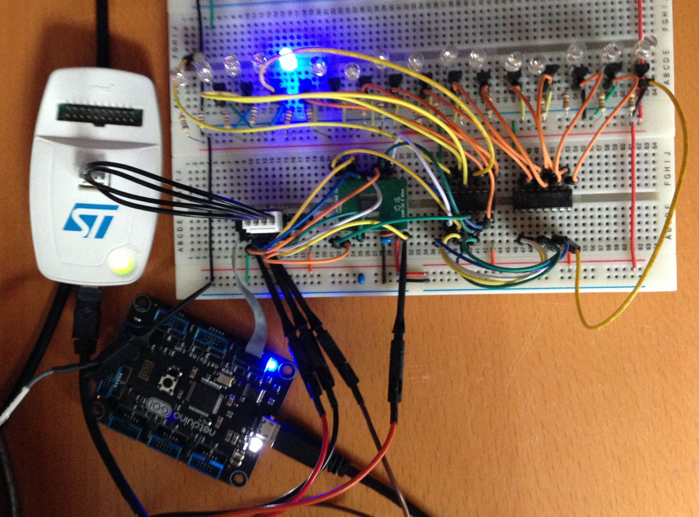
The use of SPI here actually increased the time taken (597uS Bit-Banging c.f. 795uS for 250 KHz SPI) to reliably send the grey scale data to the TLC5940. I suspect that the time can be decreased if the circuit was taken from breadboard and put onto a PCB manufactured for the purpose. The breadboard for this circuit currently looks like this:

Bread Board And Flying Leads
As you can see, there is a lot of opportunity for interference with all those flying leads.
While the time taken might have increased, the load on the microcontroller will have decreased as the SPI method is interrupt driven. The actual transmission is off-loaded to the microcontrollers dedicated circuitry.
As usual, the source code for this project is available to download.