Making a Netduino GO! Module – Stage 1 – Breadboard Prototype
So the first stage in the development process (now we have the concept) is to develop a working prototype on breadboard. This will show if we can make the hardware and software work as we want to achieve the desired goals.
Connecting up a Single 74595
For the first stage we will connect up a single 74HC595 shift register to a STM8S chip and write some software for the chip. We are not going to consider connecting the STM8S to other chips/controllers at the moment, we are simply going to output some known data to the shift register and see how it responds.
As this is a simple digital output board we can show the output from the system by using some LEDs. This will also allow us to test one of the secondary objectives, namely the ability to control a reasonable amount of current. The standard 74HC595’s will supply/sink up to 25mA per pin. However, the chip is only rated at 150mW. Turning on all of the pins will over drive the chip. So to get around this we will drive the LEDs through a transistor/MOSFET.
Breadboard Prototype
Looking at the data sheet for the 74HC595 we have 5 control signals to connect to the STM8S:
| Pin Name | Pin Number | Description |
| SI | 14 | Serial data input |
| SCK | 11 | Serial clock signal |
| /G or /OE | 13 | Output enable |
| RCK | 12 | Transfer data from shift register to the latch |
| /SCLR | 10 | Clear the shift registers |
The serial input lines of the 74HC595 lend themselves to the using the SPI bus in order to send data to the shift registers. We will not be able to use SPI in this case as we will need to reserve this for communication with the Netduino Go!.
Connecting the 74HC595
The second shift register should be connected to the same signals as the first except the serial data in line. This should be connected to the serial data output line of the first shift register. In this way the data is cascaded from the first register to the second and so on. The resultant schematic looks this this:
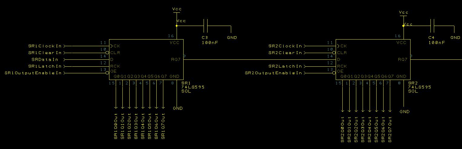
Shift Register Schematic
The next task is to connect the shift registers to the STM8S. As SPI is already reserved for communicating with the Netduino Go! the data will have to be transferred by bit-banging the data. The following connections should be made between the STM8S and the first 74HC595:
| Pin Name | 74HC595 Pin Number | STM8S Pin | Description |
| SI | 14 | Port D, Pin 2 | Serial data input |
| SCK | 11 | Port D, Pin 3 | Serial clock signal |
| /G or /OE | 13 | Port C, Pin 4 | Output enable |
| RCK | 12 | Port D, Pin 4 | Transfer data from shift register to the latch |
| /SCLR | 10 | Port C, Pin 3 | Clear the shift registers |
The above schematic becomes:
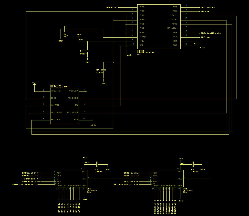
STM8S and Shift Registers Schematic
Connecting the LEDs
Visual output from the shift registers will be provided by a number of LEDs. In order to reduce the current drawn from the shift registers the LEDs will be driven by a transistor/MOSFET.
Full Circuit
When assembled, the full circuit looks something like this:

Prototype On Breadboard
Software
A small application is required to test the circuit. The first stage is to verify that the STM8S can communicate with the shift registers. The application will simply turn on the various LEDs connected to the shift registers in turn.
Firstly, we need some #define statements to make the code more readable.
#define SR_CLOCK            PD_ODR_ODR3
#define SR_DATA             PD_ODR_ODR2
#define SR_CLEAR            PC_ODR_ODR3
#define SR_OUTPUT_ENABLE    PC_ODR_ODR4
#define SR_LATCH            PD_ODR_ODR4
The application will use a small array of bytes to indicate the status of each pin on the shift register. A small helper function will allow the previous contents of the register to be cleared:
//
//  Clear all of the bytes in the registers to 0.
//
void ClearRegisters(U8 *registers, U8 numberOfBytes)
{
    for (U8 index = 0; index < numberOfBytes; index++)
    {
        registers[index] = 0;
    }
}
The final helper function will output the data to the shift registers:
//
// BitBang the data through the GPIO ports.
//
void OutputData(U8 *data, int numberOfBytes)
{
//
// Initialise the shift register by turning off the outputs, clearing
// the registers and setting the clock and data lines into known states.
//
SR_OUTPUT_ENABLE = 1; // Turn off the outputs.
SR_LATCH = 0; // Ready for latching the shift register into the storage register.
SR_DATA = 0; // Set the data line low.
SR_CLOCK = 0; // Set the clock low.
SR_CLEAR = 0; // Clear the shift registers.
__no_operation();
SR_CLEAR = 1;
//
// Output the data.
//
for (int currentByte = 0; currentByte < numberOfBytes; currentByte++)
{
U8 b = data[currentByte];
for (int index = 7; index >= 0 ; index--)
{
SR_DATA = ((b >> index) & 0x01);
SR_CLOCK = 1; // Send a clock pulse.
__no_operation();
SR_CLOCK = 0;
}
}
//
// Set the clock line into a known state and enable the outputs.
//
SR_CLOCK = 0; // Set the clock low.
SR_LATCH = 1; // Transfer the data from the shift register into the storage register.
SR_OUTPUT_ENABLE = 0; // Turn on the outputs.
}
The final code required is the main program loop which will drive the shift registers:
//
//  Main program loop.
//
void main()
{
    //
    //  Initialise the system.
    //
    __disable_interrupt();
    InitialiseSystemClock();
    //
    //  PD3 and PD2 are used for the serial data going to the registers.
    //  Configure Port D for output.
    //
    PD_ODR = 0;             //  All pins are turned off.
    PD_DDR = 0xff;          //  All pins are outputs.
    PD_CR1 = 0xff;          //  Push-Pull outputs.
    PD_CR2 = 0xff;          //  Output speeds up to 10 MHz.
    //
    //  PB4 and PB5 are used for control of the output and clearing the
    //  registers.  Configure Port B for output.
    //
    PC_ODR = 0;             //  All pins are turned off.
    PC_DDR = 0xff;          //  All pins are outputs.
    PC_CR1 = 0xff;          //  Push-Pull outputs.
    PC_CR2 = 0xff;          //  Output speeds up to 10 MHz.
    __enable_interrupt();
    //
    //  Main loop really starts here.
    //
    numberOfRegisters = 2;
    registers = (U8 *) malloc(numberOfRegisters);
    ClearRegisters(registers, numberOfRegisters);
    OutputData(registers, numberOfRegisters);
    while (1)
    {
        int counter = 0;
        while (counter < 16)
        {
            ClearRegisters(registers, numberOfRegisters);
            if (counter < 8)
            {
                registers[0] = (1 << counter);
            }
            else
            {
                registers[1] = (1 << (counter - 8));
            }
            counter++;
            OutputData(registers, numberOfRegisters);
            for (long index = 0; index < 100000; index++);
        }
    }
}
The code above turns on an LED, pauses and then moves on to the next LED. This is repeated until all of the LEDs have been illuminated. The cycle then repeats from the start. The following video shows this working:
Conclusion
At this point we have proven that the STM8S can be connected to the shift registers and we can turn on one of more LEDs connected to the output of the shift registers.
The next post in this series will connect the STM8S to the Netduino Go! and present a basic driver for the Netduino Go!, enough to illustrate that the Netduino Go! can control the shift registers.

