Making a Netduino GO! Module – Stage 3 – The Schematic
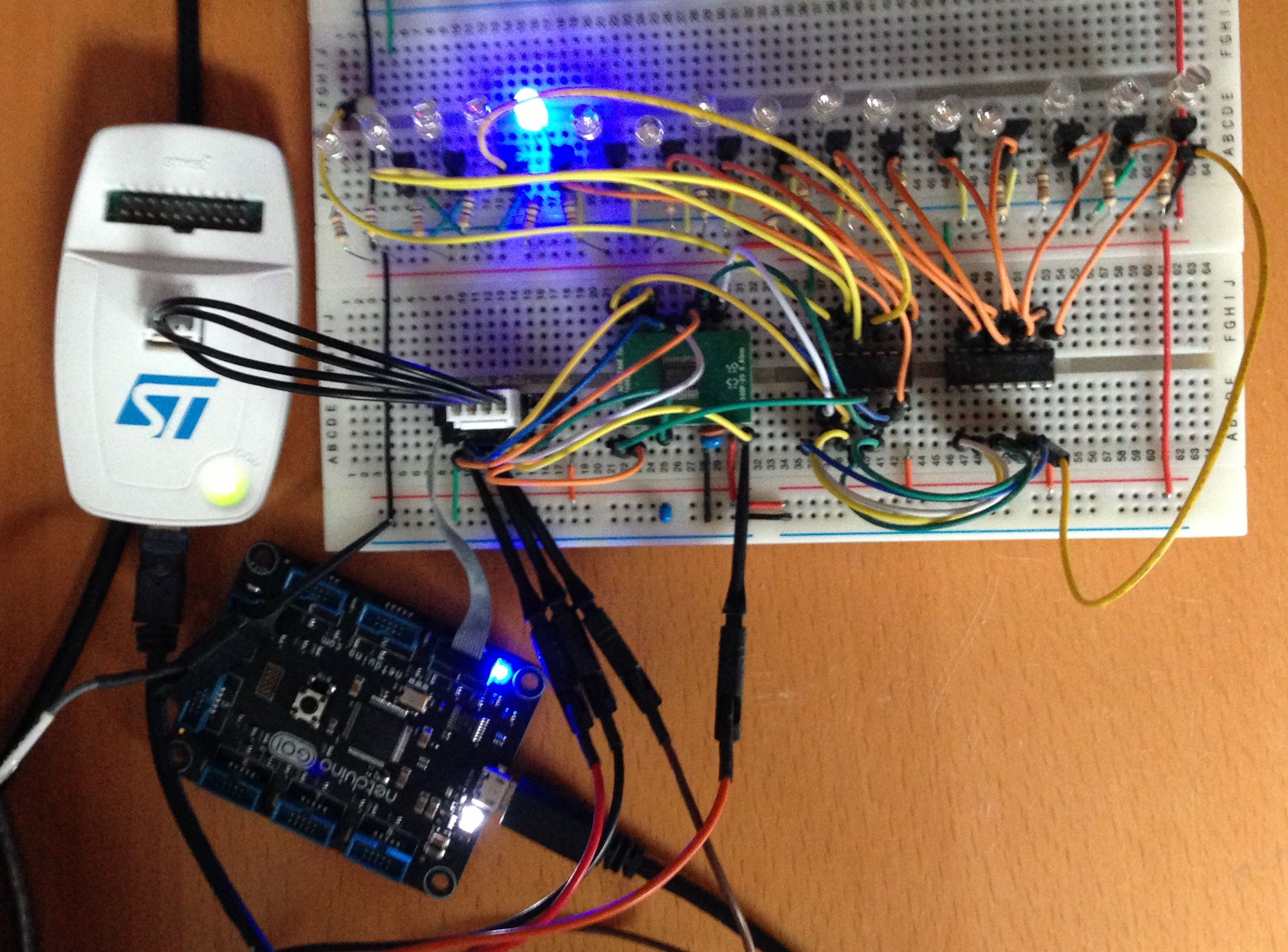
Friday, April 12th, 2013In the previous posts a prototype output expander module was put together on breadboard and connected to the Netduino Go!. A small module driver was developed for the Netduino GO! and the STM8S. This video shows the basic module working:
The next stage in the process is to make the final design decisions and produce a prototype PCB.
Design Criteria
The criteria as defined in the first post stated that the hardware should provide at least 16 digital outputs using low cost components. The breadboard prototype produced shows that we can certainly control 16 digital outputs using the common shift register.
One possible extension is to use more shift registers than were used in the breadboard prototype. This will produce a module with more outputs. A quick look at a local suppliers web site shows that these can obtained for a relatively modest cost. Adding a further two shift registers will take the outputs from 16 to 32.
The prototype shows which pin is being activated by a LED. The LED circuit includes a resistor and MOSFET/Transistor to allow the power for the LED to be provided by an external power supply rather than the 74HC595. Doing this allows the use of LEDs which would exceed the maximum power rating of the 74HC595. Although it should be possible to include these components (resistor and MOSFET) in the final design, they will be omitted in order to reduce the production costs.
In summary:
- Use the STM8S as it is low cost and powerful enough for this task
- 32 digital output (4 shift registers)
- Use 0.1" connectors to the board can be used in breadboard prototyping
PCB Design Software
Over the past few years I have spent a fair amount of time looking for the right PCB design software. I have looked at the following:
There are also several other packages available but these seem to be the three main packages offering free version of their software. Being a hobbyist price is a critical factor in the choice of software to use.
Eagle PCB is available as a free personal edition. The software and licence are both restricted in some way. I have also found the interface to be exceedingly difficult to use. As a long time user of Windows applications the interface in Eagle PCB is counter-intuitive.
KiCad is free and looks to be well supported but I found the interface difficult to use.
DesignSpark looks to be well supported and has gone through several revisions, one major revision in the time in which I have been using the software.
Of the three packages I have settled on using DesignSpark for the following reasons:
- The interface is the most "standard Windows" like of the three packages
- Free licence with no restrictions
- Eagle parts can be imported into the library
- Additional DesignSpark libraries are also available including one for Sparkfun’s components and boards
DesignSpark is not restricted to producing just the PCB design file but can also render a 3D image of the final PCB. This allows you to visualise how the final board will look. The interface allows the board to be rotated and viewed from an infinite number of points of view.
Schematic
DesignSpark is fairly intuitive to use and there are a number of tutorials and how to guides available and so I will not go into too much detail regarding using the package. There is one tip I would like to give and that is use nets.
Using nets allows the design file to be simplified greatly. You can break the design down into a number of logical components. Consider our design, this breaks down into the following three sections:
- STM8S and connector for the GoBus
- Shift registers
- Connectors for the digital outputs
Now before I discovered how the nets feature works I would have dropped the components for the STM8S and connector on the schematic and then wired them together.
Next I would have dropped the first of the shift registers onto the schematic and started to connect this to the STM8S. I would have then repeated this with the next shift register (connecting it to the first) and so on. The end result would have been a schematic which was difficult to read due to the number of connecting wires.
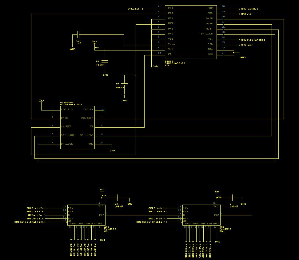
This can be simplified by the use of nets and input/output connectors/pins. So lets have a look at how this appears for the first of out logical blocks, the STM8S and the GoBus connector:
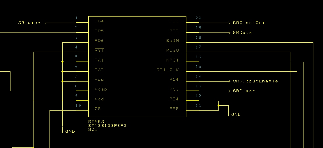
STM8S Showing Pin Labels
Looking at the above image you should note that the STM8S has two different connections, an un-named wire which goes off to another part of the circuit (i.e. pins PD5, PD6 etc.) and connections which are terminated with a name (i.e. PD3 is connected to something called SRClockOut).
The connections which go off of the image are standard interconnects between the various components on the board. These interconnects have been restricted to connecting components in our logical function block (STM8S and GoBus connector). This includes any components required to support the STM8S such as capacitors etc.
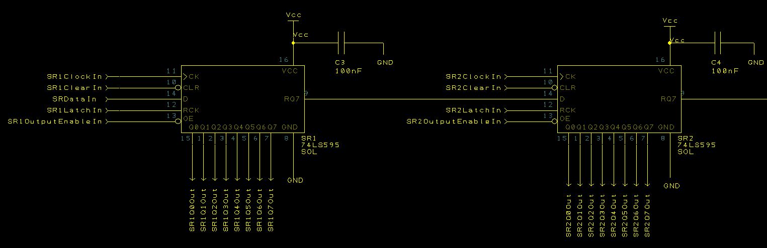
The second group of pins which go to named connections go to either an input or output pin. The names represent the function of the signal; so SRClockOut is the Shift Register Clock Output from the STM8S. If we look at the first shift register you will see that it has an input pin SR1ClockIn (Shift Register 1 Clock Input):
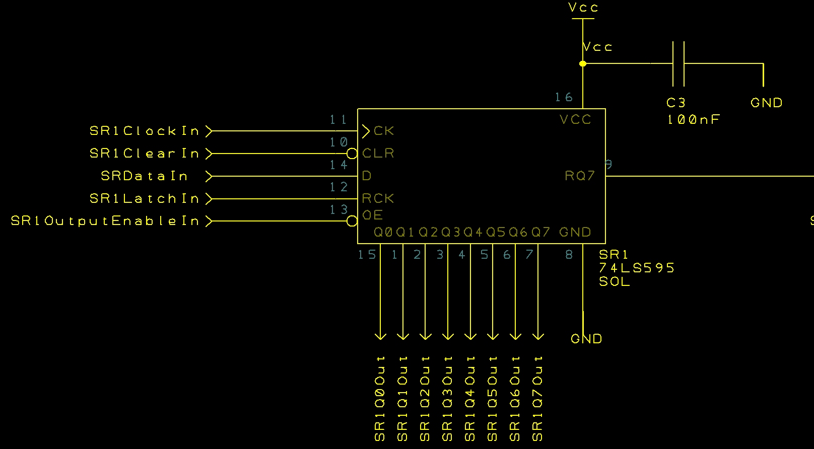
Shift Register Showing Net Names
We have two pins which have two different names but if we were to look at their properties we would find that they have both been connected to the same net, SRClock Shift Register Clock. By doing this the software knows that the two pins are in fact connected.
This process has been repeated and a number of nets have been created, some have only two pins on them (the data output from the STM8S – SRData – is only connected to the input of shift register 1), others have several (the SRClock net connected the STM8S clock output pin to the clock input of all of the shift registers).
Using nets simplifies the schematic and makes it easier to read. Using a standard naming convention for the input and output pins means that you should always be clear on which pins should be connected. It does add a new task to the design process. With a number of the pins named rather than connected you will need to verify that the pins are connected correctly.
For a small schematic like this one the process of checking the connections is relatively simple. The software allows a component (or net) to be selected from a list of all of the components/nets in the circuit. A part/net is then highlighted on the schematic once it has been selected:
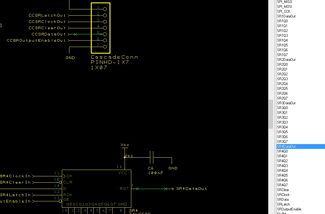
Net Selection
The above diagram shows that the net SR4DataOut has been selected; see the blue highlighted name in the list at the right of the image. The green connections on the schematic show which pins are connected to the SR4DataOut net. Checking is then a case of repeating the process for each of the nets and noting which connections are highlighted.
The final schematic for the module looks like this:
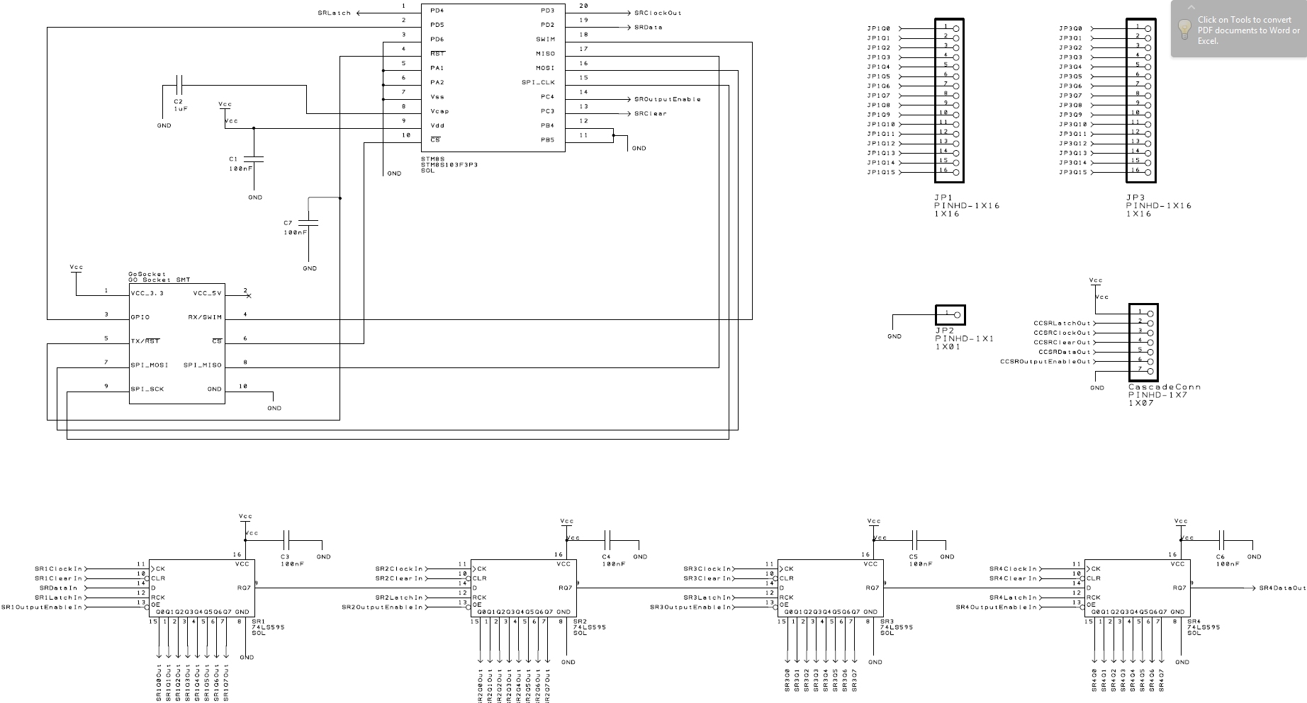
Schematic
A PDF version is also available as this may be difficult to read.
Conclusion
Now that we have the schematic we can translate this board into a PCB and from there we can get a 3D view of the board. Here is a sneak preview of the board in 3D:

Output Expander – 3D View
In the next post we shall have a look at taking the schematic and laying out the PCB.