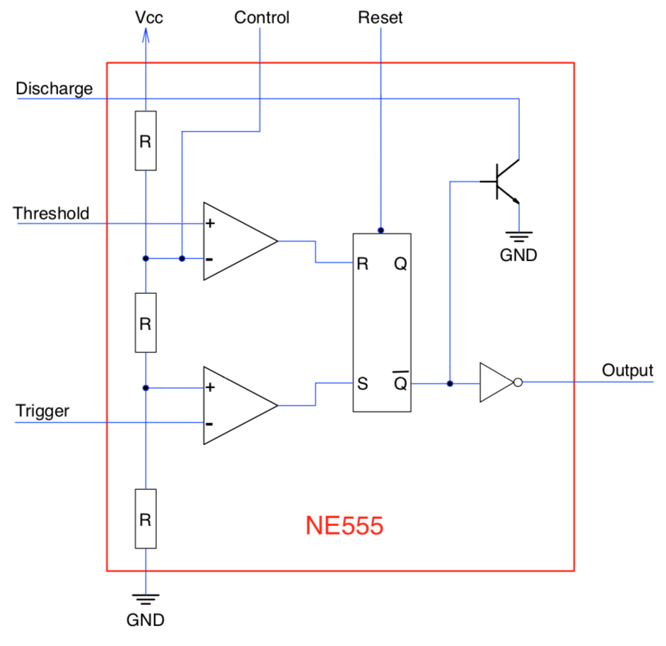
NE555 Variable Speed Clock
Sunday, February 9th, 2020The first post about the NE555 presented the theory of operation of the NE555 using an astable clock circuit. This circuit is the basis of a simple low frequency (by todays standards) digital clock or PWM circuit. A clock can be used to synchronise the various components in a digit circuit and PWM is useful in circuits for such things as light (LED) brightness.
This post will look at how the circuit in the first post can be modified to provide a variable clock for a digital circuit. A variable clock can prove useful when debugging a digital circuit.
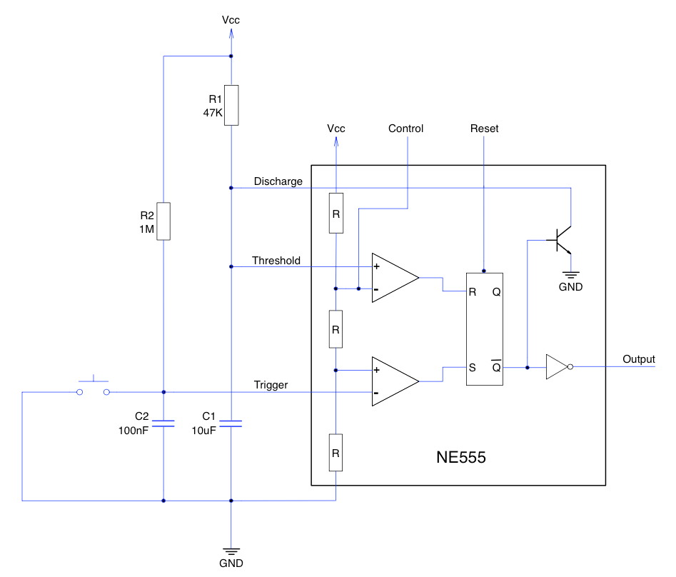
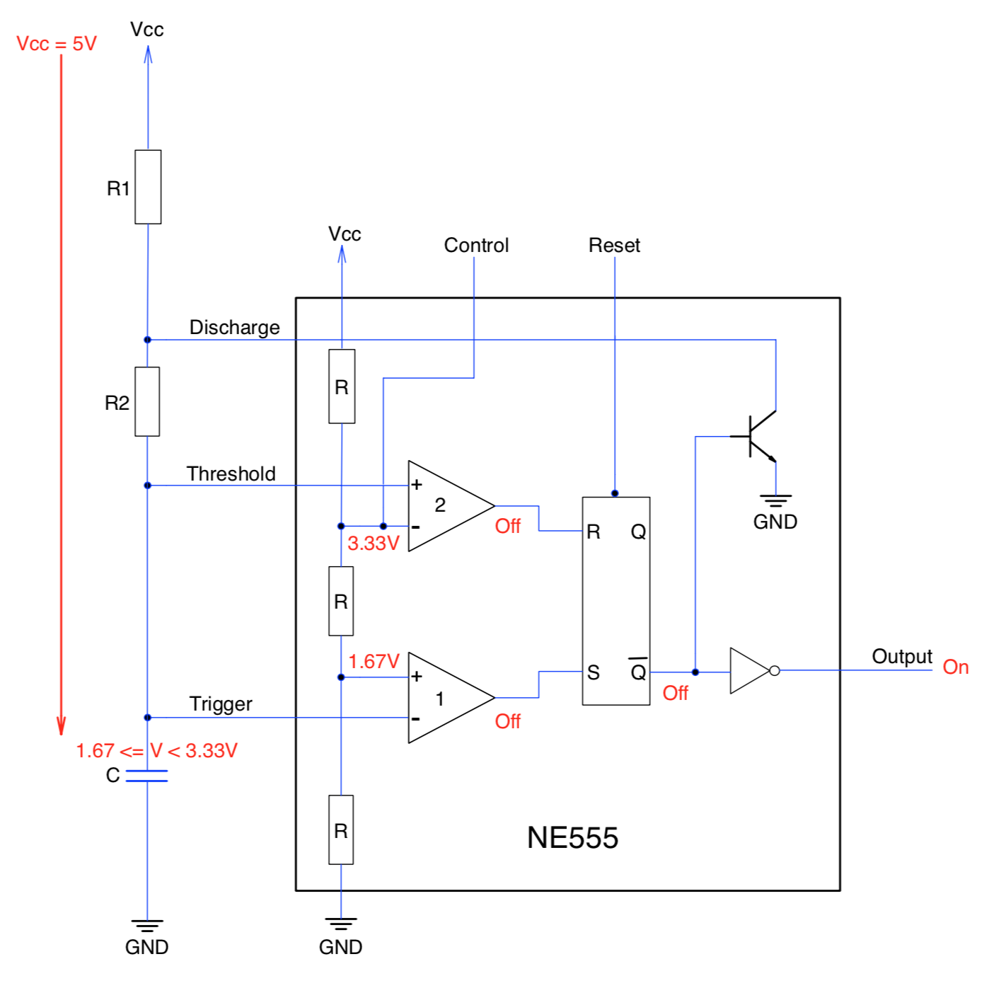
Basic Astable Circuit
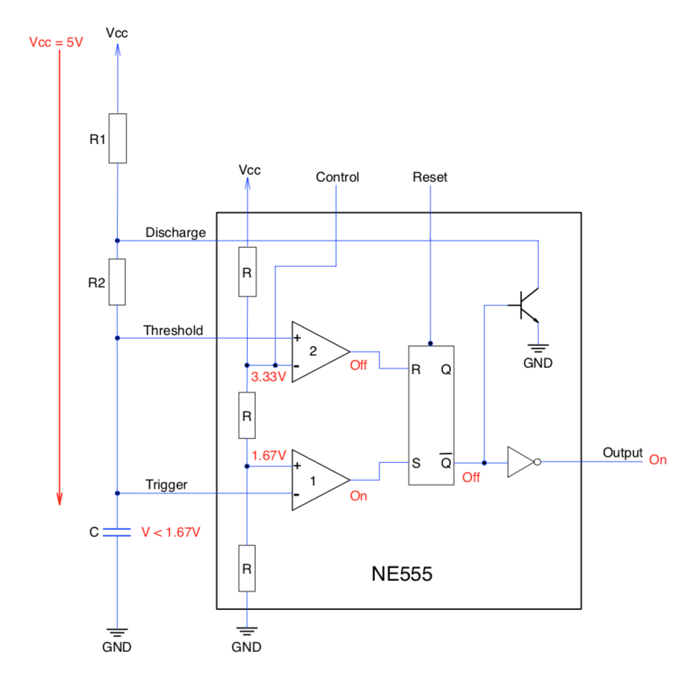
A simple astable circuit looks something like the following:

Astable Logical Layout
The two resistors R1, R2 and the capacitor control the timing and characteristics of the pulses seen on the output pin of the NE555.
Timing Calculations
The timing calculations given in the data sheet for the NE555 are as follows.
Note that in the following calculations, resistance is expressed on Ohms, capacitance in Farads and time in seconds.
Charge Time
The charge time depends upon the capacitor and the two resistors R1 and R2 as current flows through the two resistors to charge the capacitor. The time taken to charge is given as:
tcharge = 0.693 * (R1 + R2) * C
Discharge Time
The discharge time is only dependent upon the capacitor and R2 as current does not flow through R1 when the circuit is discharging. The time take to discharge is given as:
tdischarge = 0.693 * R2 * C
Period
The period is the sum of the two timings tcharge and tdischarge. This can be expressed as:
Period = 0.693 * (R1 + (2 * R2)) * C
Frequency
The frequency of a signal is defined as 1/Period. The period of a signal from an astable NE555 is:
Frequency = 1.44 / ((R1 + 2 * R2) * C)
Duty Cycle
The duty cycle of a signal is the percentage of time the signal is high compared to the period of the signal. Thus the duty cycle is given by the following formula:
Duty Cycle (%) = 100 * (R1 + R2) / (R1 + 2 * R2)
Fixed Clock
A fixed clock can be set up easily by changing one or more of the two resistors R1, R2 or the capacitor and a simple spreadsheet will allow you to calculate the circuit characteristics. Doing this allows for the creation of a low (by modern standards) frequency clock quickly and cheaply.
Variable Clock
A variable clock can be useful in debugging digital circuits. The ability to slow the speed of the system can allow the system to be probed easily while maintaining the ability to run the circuit using a free running clock.
As with a fixed clock, the clock characteristics can be changed by varying the value of one or more of R1, R2 or the capacitor.
Variable capacitors and resistors are both available but variable resistors (potentiometers) are more readily available to the hobbyist and so we will follow this option.
This gives two options, changing R1 or R2. Looking at the calculations above it is clear that R
Looking at the tdischarge formula:
tdischarge = 0.693 * R2 * C
the discharge time could theoretically be reduced to zero if R2was allowed to approach 0 Ohms. This can be prevented by replacing R2 with a combination of a fixed value resistor and a potentiometer. The fixed resistor provides for a lower limit for the discharge time of the capacitor.
A quick spreadsheet shows how the circuit will behave as R2 and C are varied:
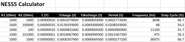
NE555 Calculations
From the results above it looks like a minimum value for R2 of 1 KOhm and a maximum of 100 KOhm would give a reasonable frequency for a low speed clock.
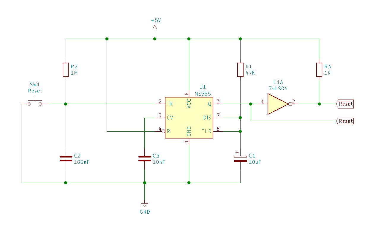
Schematic
Lowering the value of R2 1 KOhm and adding a 100 KOhm potentiometer results in the following schematic:
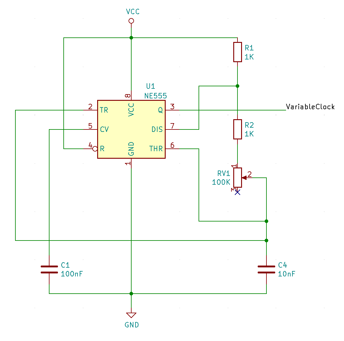
Variable Speed Clock Schematic
The value of the fixed resistor and the potentiometer gives a range of 1 KOhm to 101 KOhm. The additional 1 KOhm of resistance should not impact the frequency too much when the potentiometer is set to its maximum resistance as the calculation is dominated by the 100 KOhm potentiometer.
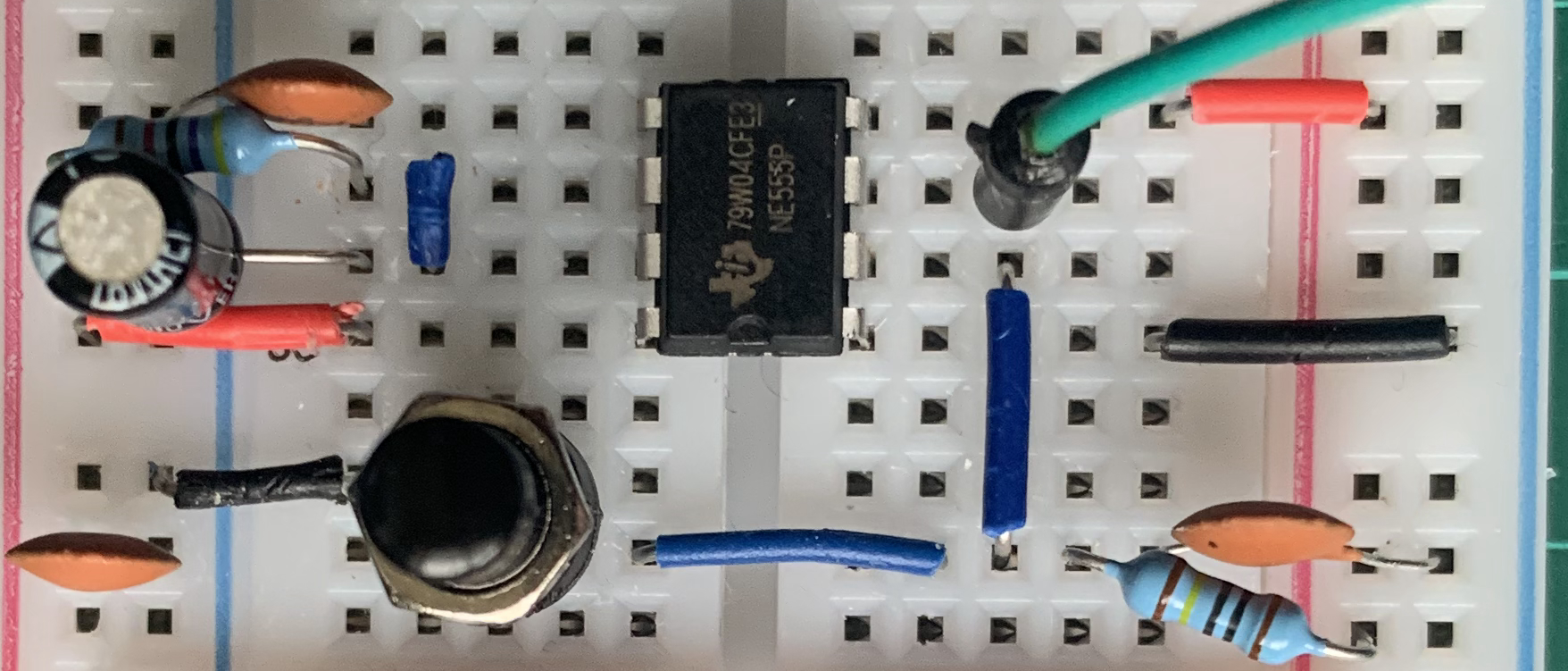
So that is the theory, how does this work in practice?
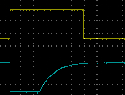
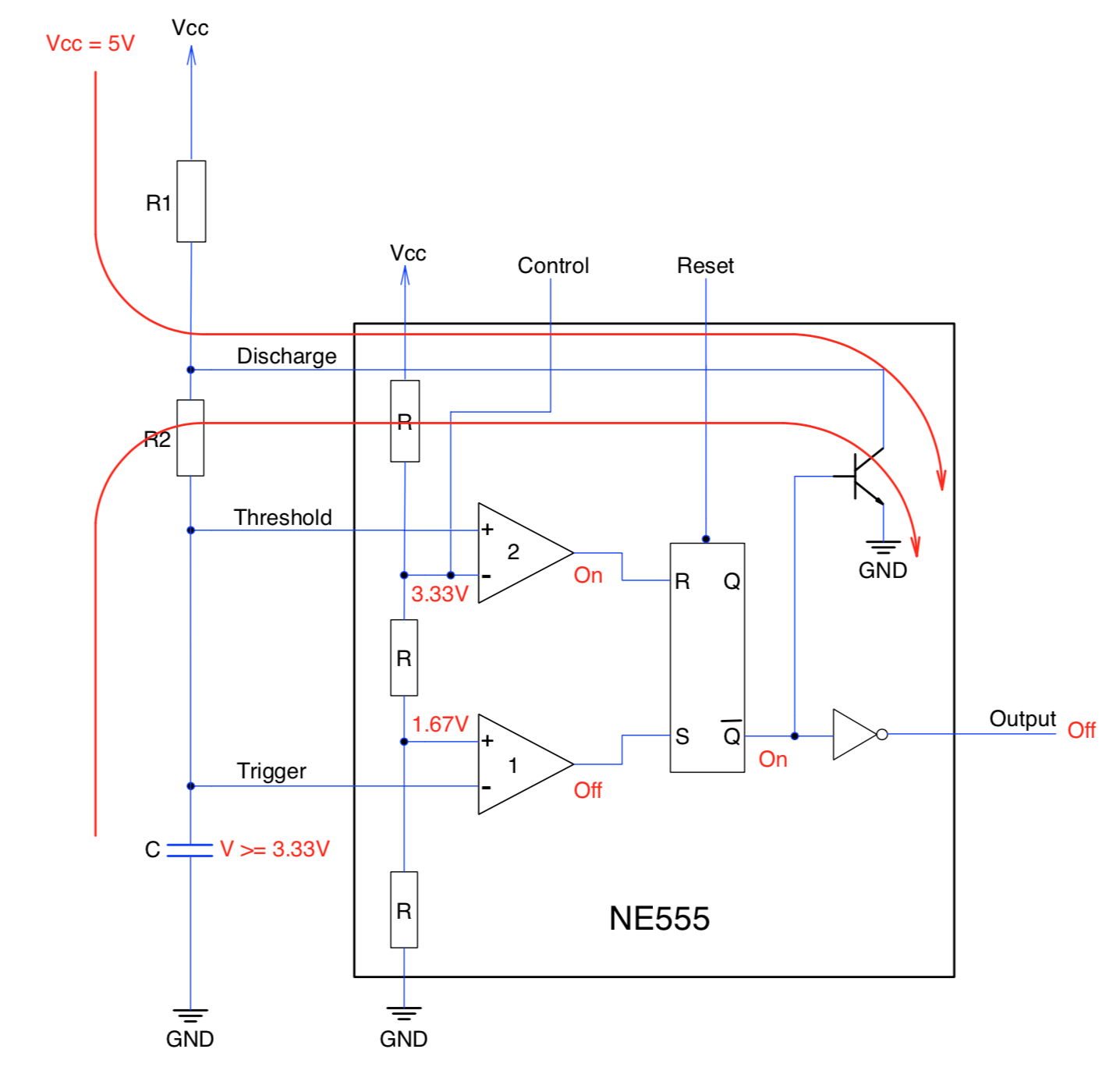
Potentiometer Set to 0 Ohms
If we set the potentiometer to 0 Ohms then according to the calculations above, the frequency should be about 48 KHz. The output on the oscilloscope is:
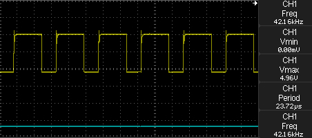
Potentiometer set to 0 Ohm
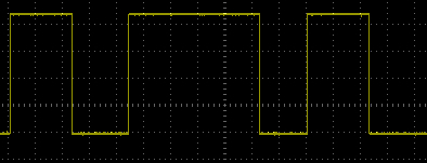
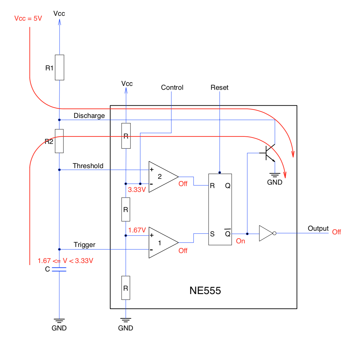
Potentiometer Set to 100 KOhms
Changing the potentiometer to 100 KOhms we should get a frequency of 712 Hz. The output on the oscilloscope is:
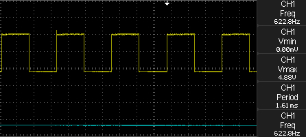
Oscilloscope output when potentiometer set to 100 KOhm
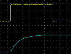
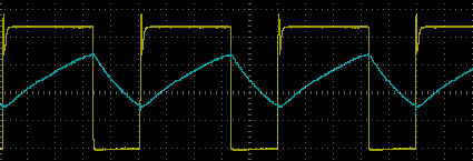
And Somewhere in the Middle
By slowly changing the resistance of the potentiometer we can achieve a steady slow clock of approximately 1 kHz:
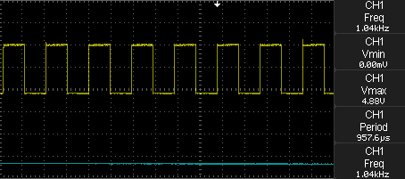
NE555 generating a 1 KHz signal
Conclusion
Clocks provide the heartbeat of most digital circuits, computers certainly require a regular pulse to synchronise the various components in the circuit. The NE555 provides a simple way to generate a variable clock albeit at low frequencies.
The output on the oscilloscope varies from the ideal values given by the calculations. This can be explained by the variations in the tolerances of the various components in the circuits and from the capacitance of the breadboard itself.