Arithmetic Logic Unit Chip Selection
In the previous post, a high level design for an Arithmetic Logic Unit (ALU) was presented. It is time to consider how this could be implemented.
7400 Series Integrated Circuits
The 7400 series of integrated circuits became a staple in computer design and digital electronics in the 1970s and 1980s. These packages implemented everything from simple logic gates (AND, OR, XOR, NOR etc.) through to complex functions such as Error Detection and Correction (see 742960). See this article for a comprehensive list of chips and their functions.
So popular were these chips that they are still available today in the original DIL (Dual In-line Package) as well as surface mount packages.
A number of variations of these ICs were produced:
| Series | Description |
|---|---|
| 74 | Standard TTL |
| 74LS | Low-power Schottky |
| 74LAS | Advanced Schottky |
| 74ALS | Advanced Low-power Schottky |
The above list is not comprehensive and many more variations are available.
This series of posts will concentrate on using the LS series of chips where possible.
Internals of the ALU
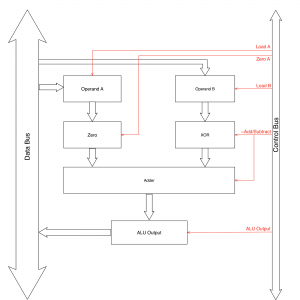
The ALU in the SSEM needs to support addition (for the JRP instruction) and subtraction (for the SUB and LDN instructions). The previous post presented the internal view of the ALU for the SSEM as:
The ALU has five distinct components:
- Storage for the A and B operands (registers)
- Zero Unit
- XOR
- Adder
- ALU Output
Let’s look at how each of these could possibly be implemented using 74LS00 series integrated circuits.
Storage for the A and B operands (registers)
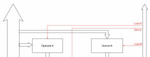
Both of the operands are connected to the data bus at the same time:
The Load control signal determines when the input signals should be stored in the register. Each of the registers holding the operand has an independent load signal. So for this part of the ALU a component is required that will:
- Take the value on the input pins and store the value
- Only load the data into the register when the trigger signal has a known value
- Present the stored value on the output pins
The above requirement fits the description of a Flip-Flop (also known as a Latch).
The 74LS00 series has a number of flip-flops and latches available. The 74LS373 contains an octal transparent latch with three state output. This chip is still commonly available and has the following properties:
- Input signals can be latched (stored) in the internal registers on request
- The output from the latch can be turned on or off, again, on request
The above functions are controlled by two signals:
- Clock
- Output Enable (~OE)
Clock
When the clock signal is low the inputs are effectively disconnected from the latches. the latches will therefore remain unchanged and hold the previously latched value.
A high clock signal will allow the input pins to the connected to the latches. Any changes on the inputs are presented to the latches. This holds true for as long as the clock signal is in the high state.
The state of the input pins is held in the latches when the clock signal transitions from high to low (on the falling edge of the clock).
Output Enable
The output enable pin is an active low pin (denoted here by the ~ symbol before the name of the pin). This means that the contents of the latches will be output from the chip when the ~OE pin is in the low state.
Putting the ~OE pin in a high state disconnects the latches from the output pins and puts the outputs in a high impedance (also known as a high-Z) state.
Setting ~OE low while the clock pin is high means that the outputs will follow the inputs. This happens because the high clock signal allows the inputs to be connected to the latches and the low output signal puts the value in the latches on to the output pins.
Loading the Latch
From the above description, the Clock pin should be connected to the Load A and Load B signals of the respective operands. This will allow the latch to be loaded with the input signals when the load signal falls from high to low.
The inputs to the chips should be connected to the data bus directly and simultaneously. Data cannot be loaded into the latch until the appropriate load signal transitions from high to low. The load signals will control when the operand changes as follows:
- Load A (or Load B) signals are low then the inputs will have no impact on the operands. The outputs will reflect the previous value stored in the latch.
- When Load A (or Load B) is high then the contents of the data bus will be presented to the respective latch. The output of the respective operand will reflect the current contents of the data bus.
- When the Load A (or Load B) signal falls from high to low, the current contents of the data bus will be stored in the respective operand. The output will reflect this value no matter what happens on the data bus.
Aside: in 2013, the intention was to simulate the SSEM in VHDL. The 74HC373 was simulated in a series of posts around that time.
XOR
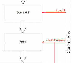
The next block available is the 74LS series is the XOR block:
This block performs one part of the negation process allowing the adder to also perform subtraction. The XOR truth table is:
| ~Add/Subtract | Input Value | Output |
| 0 | 0 | 0 |
| 0 | 1 | 1 |
| 1 | 0 | 1 |
| 1 | 1 | 0 |
In twos complement, the first part of generating a negative number is to invert the bits in the original number. If you examine the above truth table, when the ~Add/Subtract signal is low, the output reflects the input value. When ~Add/Subtract is high then the output is the inverse of the input value.
| ~Add/Subtract | Operation |
| 0 | Add |
| 1 | Subtract |
So, setting the ~Add/Subtract signal high when the ALU is subtracting operand B from operand A and low when the ALU is adding operand A to operand B will ensure that the correct value is passed through to the adder.
The 74LS86 is a quad 2-input XOR gate (contains four 2-input XOR gates) in a single package. The necessary functionality is achieved by connecting the A inputs (not to be confused with the A operand) of each gate to the ~Add/Subtract signal. All of the A inputs are therefore connected together. The B inputs are connected to the outputs of the B operand latch.
Zero
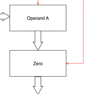
The zero unit sits between the output of the A operand and the Adder. Its function is to select between two possible input values:
- Zero
- A operand
and pass the selection on to the Adder.
A number of possibilities exist:
- Use the ~OE signal on the A output to simply turn the output off when zero is required. This may require the use of pull down resistors to prevent a floating signal.
- Use a buffer chip such as the 74LS245 to connect the Adder to ground when ~OE on the A operand goes high
A little investigation is required.
Adder
The adder unit takes the inputs and simply adds them together:
The 74LS283 is a four bit full adder with carry in and carry out. An 8-bit adder is created by chaining two four bit adders together:
In the case of subtraction, the final part of the negation of a twos complement number is to add 1 to the inverted bit pattern of the original number. Setting the carry in on the first adder effectively adds one to the number. The same ~Add/Subtract signal in the XOR block can be used here as it is low for addition (zero will be added to the sum) and high for subtraction (one will be added to the sum).
ALU Output
The ALU output takes the output of the adder and makes this available to the data bus:
Output to the data bus is controlled by the ALUOutout signal and this function can be performed by a buffer circuit. The 74LS245 is an octal bus transceiver with non-inverting three state outputs. The direction of signal transmission can be controlled using the DIR pin on this chip. In the case of the ALU, the direction is always from the ALU to the data bus and so this pin can be held high (or low) permanently.
Output from 74LS245 is controlled by the ~OE pin. This is an active low pin and the chip is transparent when the signal is low and in high impedance mode when this pin is held high.
Conclusion
All of the integrated circuits for the high level functionality of the ALU have been identified. The next step is to put this together and see if it works as expected.
Something for the next article.
Tags: Electronics, Home Built CPU
Sunday, July 16th, 2017 at 9:08 am • Electronics, Home Built CPU • RSS 2.0 feed Both comments and pings are currently closed.


