RSS

Posts Tagged ‘STM8’

Using Registers on the STM8S

Saturday, June 23rd, 2012

A few weeks ago I had a rant about the STM8S Standard Peripheral library after it cost me a fair amount of time tracking down what appeared to be a bug in the library. As a result of this I have moved over to accessing the registers on the chip directly to control the operation of the chip. A recent question ion one of the forums I haunt has prompted this post. Here I am going to present a few different ways of achieving the same task, one using the STD Peripheral Library and two examples using the registers directly but in different ways.

The task we are going to be looking at is one I perform as part of my initialisation of the STM8S, namely I set the clock up to a known state. In this case we will be setting the system to use the HSI clock running at 16 MHz with no dividers.

It is important to note that you will need to have a copy of the reference manual for the chip available when using direct register access to control the microcontroller. In this case you should be looking for document RM0016 on ST’s web site.

Using the Standard Peripheral Library

Using the STD Peripheral Library makes this a relatively simple task. We only need to call four methods:

CLK_DeInit();
CLK_SYSCLKConfig(CLK_PRESCALAR_CPUDIV1);    // CPU Prescalar = 1.
CLK_SYSCLKConfig(CLK_PRESCALAR_HSIDIV1);    // Prescalar = 1, 16 MHz.
CLK_ClockSwitchConfig(CLK_SWITCHMODE_AUTO,  // Automatically switch
                      CLK_SOURCE_HSI,       // Switch to internal timer.
                      DISABLE,              // Disable the clock switch interrupt.
                      CLK_CURRENTCLOCKSTATE_DISABLE);   // Disable the previous clock.

The headers for the above methods can be found in the file stm8s_clk.h and the source code for the methods can be found in the file stm8s_clk.c. These source files can be found in the source code folder of the STD Peripheral Library.

Direct Register Access – Method 1

This first method of accessing the registers continues to use the STD Peripheral Library files but we do not make any calls into the library. Instead we use the definitions for the registers to access the chip directly.

So let’s start by breaking the above four methods down into their direct register equivalents.

CLK_DeInit

The first thing we need to do is to reset all of the registers to the default values:

CLK->ICKR = CLK_ICKR_RESET_VALUE;
CLK->ECKR = CLK_ECKR_RESET_VALUE;
CLK->SWR  = CLK_SWR_RESET_VALUE;
CLK->SWCR = CLK_SWCR_RESET_VALUE;
CLK->CKDIVR = CLK_CKDIVR_RESET_VALUE;
CLK->PCKENR1 = CLK_PCKENR1_RESET_VALUE;
CLK->PCKENR2 = CLK_PCKENR2_RESET_VALUE;
CLK->CSSR = CLK_CSSR_RESET_VALUE;
//
//  The following set has to be performed twice.
//
CLK->CCOR = CLK_CCOR_RESET_VALUE;
while ((CLK->CCOR & CLK_CCOR_CCOEN) != 0);
CLK->CCOR = CLK_CCOR_RESET_VALUE;
CLK->HSITRIMR = CLK_HSITRIMR_RESET_VALUE;
CLK->SWIMCCR = CLK_SWIMCCR_RESET_VALUE;

As you can see, the library certainly hides a large amount of work from you. Most of the above code is simply a case of setting up the registers to default values.

To find out how this all works you need to start looking in the stm8s.h file. A quick search for CLK soon leads you to the following type declaration:

typedef struct CLK_struct
{
  __IO uint8_t ICKR;     /*!> Internal Clocks Control Register */
  __IO uint8_t ECKR;     /*!> External Clocks Control Register */
  uint8_t RESERVED;      /*!> Reserved byte */
  __IO uint8_t CMSR;     /*!> Clock Master Status Register */
  __IO uint8_t SWR;      /*!> Clock Master Switch Register */
  __IO uint8_t SWCR;     /*!> Switch Control Register */
  __IO uint8_t CKDIVR;   /*!> Clock Divider Register */
  __IO uint8_t PCKENR1;  /*!> Peripheral Clock Gating Register 1 */
  __IO uint8_t CSSR;     /*!> Clock Security System Register */
  __IO uint8_t CCOR;     /*!> Configurable Clock Output Register */
  __IO uint8_t PCKENR2;  /*!> Peripheral Clock Gating Register 2 */
  uint8_t RESERVED1;     /*!> Reserved byte */
  __IO uint8_t HSITRIMR; /*!> HSI Calibration Trimmer Register */
  __IO uint8_t SWIMCCR;  /*!> SWIM clock control register */
}
CLK_TypeDef;

If you have a look at the technical reference sheet for the chip, you will find section which shows the memory layout for the registers. These are at fixed locations in memory and should map to the above layout. The __IO is defined as volatile and will prevent the compiler from optimising out any references to the variables.

The next thing to note is that we still do not have a definition for CLK. A little more searching in the same file will lead you to the following statement:

#define CLK ((CLK_TypeDef *) CLK_BaseAddress)

So this defines CLK for us as a pointer to a location in memory. Some more searching (again in the same file) leads us to the following line of code:

#define CLK_BaseAddress         0x50C0

So the code CLK->ICKR = 0; will set the register at location 0x50C0 to zero.

One point to note is the statement while ((CLK->CCOR & CLK_CCOR_CCOEN) != 0);. This illustrates the use of another type of declaration you will find in stm8s.h, namely, CLK_CCOR_CCOEN. This declaration allows you to mask off certain bits within a register and use this to set or check values in a register. The name is made up of three parts:

NameDescription
CLKClock registers are being access.
CCORThis relates to the CCOR register.
CCOENMask the CCOEN bits in the register.

CLK_SYSCLKConfig

The next task is to set the prescalar for the system clock. This is being set to 1 to ensure the system runs at 16 MHz.

CLK->CKDIVR  &= (uint8_t) (~CLK_CKDIVR_HSIDIV);
CLK->CKDIVR |= (uint8_t) ((uint8_t) CLK_PRESCALAR_HSIDIV1 & (uint8_t) CLK_CKDIVR_HSIDIV);

The first line resets the prescalar to a known value whilst the second selects the divider which will be used.

CLK_ClockSwitchConfig

The final operation is to switch the system clock to the HSI and this is achieved with the following code:

CLK->SWCR |= CLK_SWCR_SWEN;
CLK->SWCR &= (uint8_t) (~CLK_SWCR_SWIEN);
CLK->SWR = (uint8_t) CLK_SOURCE_HSI;
uint16_t downCounter = CLK_TIMEOUT;
while ((((CLK->SWCR & CLK_SWCR_SWBSY) != 0 ) && (downCounter != 0)))
{
    downCounter--;
}

Direct Register Access – Method 2

This method uses the register declarations found in the header files provided by IAR. So for the STM8S103F3 we will be looking in the file .

CLK_DeInit

As before, the first thing we will do is to reset the registers to a known set of values:

CLK_ICKR = 0;
CLK_ECKR = 0;
CLK_SWR = 0xe1;
CLK_SWCR = 0;
CLK_CKDIVR = 0x10;
CLK_PCKENR1 = CLK_PCKENR1_SPI | CLK_PCKENR1_TIM2;   //  Enable the peripheral clocks we need.
CLK_PCKENR2 = 0;
CLK_CSSR = 0;
CLK_CCOR = 0;
while (CLK_CCOR_CCOEN != 0);
CLK_CCOR = 0;
CLK_HSITRIMR = 0;
CLK_SWIMCCR = 0;

The first thing you will notice is that by using this method we are not using the pointer dereferencing operator. Instead the application is accessing the registers directly. So let’s have a look at the header file and dissect the reset of the ICKR register. Searching for CLK_ICKR leads us to the following code:

typedef struct
{
  unsigned char HSIEN       : 1;
  unsigned char HSIRDY      : 1;
  unsigned char FHW         : 1;
  unsigned char LSIEN       : 1;
  unsigned char LSIRDY      : 1;
  unsigned char REGAH       : 1;
} __BITS_CLK_ICKR;
__IO_REG8_BIT(CLK_ICKR,    0x50C0, __READ_WRITE, __BITS_CLK_ICKR);

The first things we see is the definition of the structure which maps on to the format of the ICKR register. Each bit field is broken out and maps on to the sections of the register as defined in the data sheet.

The final line of code in the above snippet uses the __IO_REG8_BIT macro to map the data structure onto the address 0x50C0 and create a new name with bit level access.

The next thing to note is the while loop which checks the CCOOEN bit in the CCOR register – while (CLK_CCOR_CCOEN != 0);. As above, this uses a three part notation to form a reference, this time it is to a particular bit in a register. This is not a mask as in the previous example. This is broken down as follows:

NameDescription
CLKClock registers are being access.
CCORThis relates to the CCOR register.
CCOENCCOEN bits in the CCOR register.

Some more digging in the file leads to the following definition:

#define CLK_CCOR_CCOEN           CLK_CCOR_bit.CCOEN

The CLK_CCOR_bit declaration was created by the __IO_REG8_BIT macro. This is the name which has been given to the location in memory of the ICKR register.

CLK_SYSCLKConfig

The next task is to set the prescalar for the system clock. This is being set to 1 to ensure the system runs at 16 MHz. Note that a prescalar of 1 maps to the prescalar bits in the register being set to zero.

CLK_CKDIVR = 0;

CLK_ClockSwitchConfig

The final operation is to switch the system clock to the HSI and this is achieved with the following code:

CLK_SWCR_SWEN = 1;
CLK_SWR = 0xe1;                     //  Use HSI as the clock source.
while (CLK_SWCR_SWBSY != 0);        //  Pause while the clock switch is busy.

Conclusion

So there you have it, three different ways of performing the same task. The method used will be down to individual preference. Happy experimenting.
Using the UART on the STM8S

Friday, June 8th, 2012

If you have been reading my recent posts you will have noticed that I have had some problems setting up the UART on the STM8S. IN fact I spent several days getting this working. This post gives a couple of code snippets which I have used to get around this problem. You may need to refer to the data sheet on the processor for more detail on how this code works.

Setting Up the UART

This code makes a fundamental, namely that you have configured the chip and your circuit to run at 16 MHz. I did this by setting the chip to use the internal oscillator as it’s clock source and using a prescalar of 1. If you have this set up then the following method will allow you access to the UART running at 115200 baud, 8 data bits, 1 stop bit and no parity.

Firstly, we need to make sure we are using the right include files:

#include "stm8s.h"
#include "stm8s_uart1.h"

Next we need to set up the port:

void SetupSerialPort()
{
    //
    //  Clear the Idle Line Detected bit in the status register by a read
    //  to the UART1_SR register followed by a Read to the UART1_DR register.
    //
    (void) UART1->SR;
    (void) UART1->DR;

    UART1->CR2 = UART1_CR2_RESET_VALUE;
    UART1->CR4 = UART1_CR4_RESET_VALUE;
    UART1->CR5 = UART1_CR5_RESET_VALUE;
    UART1->GTR = UART1_GTR_RESET_VALUE;
    UART1->PSCR = UART1_PSCR_RESET_VALUE;
    //
    //  Setup the port.
    //
    UART1->CR1 = (u8) UART1_WORDLENGTH_8D | (u8) UART1_PARITY_NO;   // Word length = 8, no parity.
    UART1->CR3 = (u8) UART1_STOPBITS_1;                             // 1 stop bit.

    UART1->BRR1 &= (uint8_t) (~UART1_BRR1_DIVM);
    UART1->BRR2 &= (uint8_t) (~UART1_BRR2_DIVM);
    UART1->BRR2 &= (uint8_t) (~UART1_BRR2_DIVF);
    //
    //  Set the clock prescaler for 11520 baud.  This assumes a 16 MHz clock speed.
    //
    UART1->BRR2 = 0x0b;
    UART1->BRR1 = 0x08;
    //
    //  Disable the Transmitter and Receiver before seting the LBCL, CPOL and CPHA bits
    //
    UART1->CR2 &= (u8) ~(UART1_CR2_TEN | UART1_CR2_REN);
    //
    //  Clear the Clock Polarity, lock Phase, Last Bit Clock pulse
    //
    UART1->CR3 &= (u8)~(UART1_CR3_CPOL | UART1_CR3_CPHA | UART1_CR3_LBCL);
    //
    //  Set the Clock Polarity, lock Phase, Last Bit Clock pulse
    //
    UART1->CR3 |= (u8)((u8) UART1_SYNCMODE_CLOCK_ENABLE &
                       (u8) (UART1_CR3_CPOL | UART1_CR3_CPHA | UART1_CR3_LBCL));
    //
    //  Set the Tx and Rx state
    //
    UART1->CR2 |= (u8) ((u8) UART1_CR2_TEN | (u8) UART1_CR2_REN);
    UART1->CR3 &= (u8) (~UART1_CR3_CKEN);
}

Having set up the UART we need a method to write data to the port. The following method will send simple text strings to the UART:

//
//  Send a message to the debug port (UART1).
//
void Printf(char *message)
{
    char *ch = message;
    while (*ch)
    {
        UART1->DR = (u8) (*ch);
        while ((UART1->SR & (u8) UART1_FLAG_TXE) == RESET);
        ch++;
    }
}

Using the UART

The use of this code can be illustrated by the following program:

void main()
{
    SetupSerialPort()
    Printf("Hello from my program");
}

ST’s Standard Peripheral Library – A Day in my Life I’ll Never Get Back

Wednesday, June 6th, 2012

A couple of days ago I was working on a project and was having some problems debugging. It was nothing to do with the debugging environment more to do with the high speed interaction between two devices. So I needed some debug output – enter UART1. I decided that I would send some debug information to UART1 and capture this in PuTTY. At least I would be able to see the sequence of events and hopefully work out where my code is going wrong.

This is where my problems started…

UART Examples

So I started looking through the Standard Peripheral Library example programs. Sure enough there is a program there in the directory UART1_Printf Sounds ideal, I should be able to throw some text data at this and have it appear in PuTTY. Great.

Quick check of the readme.txt in this directory and it looks like this program is compatible:

Hardware and Software environment

This example runs on STM8S High density and Low density devices and on STM8A High density devices.

So I am running on the STM8S103F3 which is one of the low density STM8 devices so I should be fine with this code. A little further down the file it gives the specification for the serial comms as:

Hyperterminal configuration:

  • Word Length = 8 Bits
  • One Stop Bit
  • No parity
  • BaudRate = 115200 baud
  • flow control: None

Great – we are in business!

So what happened?

Creating a project was simple and I had the code compiling within a few minutes. Next job is to hook up PuTTY and send some data through down the serial connection and see it appear on the PC. This is where life got a little messy. Nothing appeared. Double checked all of the settings in both the program and Putty – they both match. Ahhh – should Tx and Rx be crossed? No that did not work.

Hmmmmmmmm….. This could be a long day.

Next step, break out the trusty logic analyser from Saleae. Connected this up and managed to show that data was in fact being output from the application but at 53 baud. This is a long way from the 115200 baud promised.

Hmmmm, so lets change the baud rate requested – 9600 baud is normally safe. No change, still 53 baud.

Starts clutching at straw, lets just make sure the system clock is running using the HSI 16 MHz signal. Still no joy, 53 baud is all I seem to be getting.

The Problem

I finally broke out the data sheet for the chip and started single stepping through the STD Peripheral library code. The example program contains the following line of code:

UART1_Init((uint32_t)115200, UART1_WORDLENGTH_8D, UART1_STOPBITS_1, UART1_PARITY_NO,
UART1_SYNCMODE_CLOCK_DISABLE, UART1_MODE_TXRX_ENABLE);

This should set up the port to operate at the rates as per the read me file. If you have a look at this method, about half way down you will see the following code:

/* Set the UART1 BaudRates in BRR1 and BRR2 registers according to UART1_BaudRate value */
BaudRate_Mantissa    = ((uint32_t) CLK_GetClockFreq() / (BaudRate << 4));
BaudRate_Mantissa100 = (((uint32_t) CLK_GetClockFreq() * 100) / (BaudRate << 4));
/* Set the fraction of UART1DIV  */
UART1->BRR2 |= (uint8_t)((uint8_t)(((BaudRate_Mantissa100 - (BaudRate_Mantissa * 100)) << 4) / 100) & (uint8_t)0x0F);
/* Set the MSB mantissa of UART1DIV  */
UART1->BRR2 |= (uint8_t)((BaudRate_Mantissa >> 4) & (uint8_t) 0xF0);
/* Set the LSB mantissa of UART1DIV  */
UART1->BRR1 |= (uint8_t) BaudRate_Mantissa;

So I am single stepping through the code and notice something odd, the Baud Rate Registers (BRR1 and BRR2) are not being set correctly. By my calculations these should be 0x68 and 0x03 respectively (for 9600 baud).

A quick modification to the source file to put these explicit changes in and….

It Works !

I now have PuTTY talking to my STM8 at 9600 baud and so my debugging life should be a little easier. On the downside, I have lost a little faith in the Standard Peripheral Library. I think that in future I will be using this more for guidance rather than as a method of programming this family of processors. Coupled with the data sheet for the chip is is going to be an invaluable tool. Going forward I will be building up my own set of methods working with the registers on the processor. This may be slower but it will bring me closer to the chip and I may occasionally come across the odd gem in the data sheet which I may not otherwise have become aware of.

Now, back to the original problem.

4 Digit, 7 Segment Display

Thursday, May 17th, 2012

In early May I started working on a module to display a 4 digit number on a 7 segment LED display. I developed this as far as a working proof of concept developing the hardware and software necessary to prove that the module was feasible. At this point I discovered that development was ongoing by two other teams and decided to stop development at this point taking what I had learnt onboard and move on to other projects.

This article presents the work so far as this is a working project and demonstrates some of the principles used in the STM8S articles written so far this month. Namely:

  • GPIO output
  • Timers

As already stated, this project is working but incomplete and there is no intention to take the hardware further than the proof of concept as presented here.

Hardware Design

The system will use four 7-segment LED modules in place of a single 4 digit, 7 segment module. The hardware design requires the following circuit components:

  • Microprocessor controller
  • Power supply to the 7-segment display modules
  • Decoding for the 7-segments

The software will use multiplexing to allow one chip to be used to control the four 7-segment modules. The basic process is as follows:

  1. Turn power to all segments off
  2. Send the data for a digit to the 74LS47 chip
  3. Turn on the power for the digit
  4. Wait a short time
  5. Move on to the next digit and go back to start

This will give the illusion that all of the LEDs are powered all of the time.

Microcontroller

The microcontroller chosen was the STM8S003 as this is supported by the Netduino team for designers who wish to create their own modules. This chip has several free development environments available and the IAR environment has been used in this blog to document several small projects using this family of chips.

The project as it stands requires the use of 9 pins from the STM8S. Four pins will be used for power control, one line per digit. A further four pins will be used to tell the 74LS47 which of the segments are to be lit. The final pin will be used to indicate if the digit zero is to be shown for a zero value. More on this in the decoding section below. The use of this number of pins makes this unsuitable as it stands for use as a Netduino GO! module. Further refinement is required to take this forward as a module.

7-segment Power Control

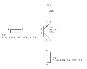
The LED power is controlled by using a PNP transistor (the 7-segments share a common anode). In this circuit the power is run through a single current limiting resistor. This will mean that numbers with few digits (for example, 1) will be displayed more brightly then those with a large number of segments (say 8). The final circuit would need to refined to have a current limiting resistor per segment or using a constant current driver. This component of the circuit looks like this:

Power control for a single 7-segment LED module.

The resistor R5 is connected to the output of the microcontroller and the output of R9 going through to the power pin on the 7-segment display.

Decoding the 7-segments

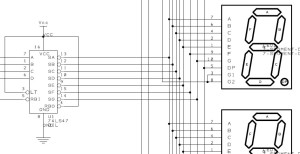
The decoding of the output from the microcontroller is performed by the 74LS47 chip. This is a dedicated decoder circuit for common anode 7-segment LED modules. The system takes a binary coded decimal number and then sinks the current from the appropriate segments of the display. The result is that the module will display the appropriate digit.

We will also take advantage of one final line, the RBI line. By turning this line on and off we can determine if the digit will display the digit 0 when the input to the decoder is zero. So why would we change this line? We we could fix the line so that a digit will always be displayed. So when the microcontroller wants to show 0 it will actually show either a blank display or 0000. The blank display is obviously not desirable as the user will not be able to determine if the display is showing 0 or if it is turned off. Showing four zeroes will give the user the correct information. A nicer solution is for the display to show a single zero when the microcontroller outputs 0.

The resulting decoder wiring looks something like the following:

7-segment decoder circuit

Where pins A, B, C and D will output the binary version of the digit to be displayed.

Full Circuit

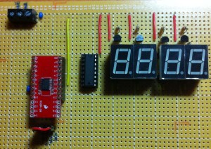
This PDF File contains the full circuit diagram for the proof of concept module. The fully assembled circuit looks like this:

Prototype Circuit

Software

In order to test the circuit we will write a small program which will start at 0 and count to 9999 before returning to 0 and starting counting again.

The first thing we need to do is to initialise the system. The following code resets the system clock source, configures the GPIO lines and then starts the timer which contain the code which will perform the multiplexing.

//
//  Initialise the clock
//
CLK_DeInit();
CLK_SYSCLKConfig(CLK_PRESCALER_CPUDIV1);                // CPU Prescaler = 1.
CLK_SYSCLKConfig(CLK_PRESCALER_HSIDIV1);                // Prescaler = 1, 16 MHz.
CLK_ClockSwitchConfig(CLK_SWITCHMODE_AUTO,              // Automatically switch
					  CLK_SOURCE_HSE,                   // Switch to internal timer.
					  DISABLE,                          // Disable the clock switch interrupt.
					  CLK_CURRENTCLOCKSTATE_DISABLE);   // Disable the previous clock.
//
//  Initialise GPIOs
//
GPIO_DeInit(GPIOC);
GPIO_Init(DIGIT0_BI_PORT, DIGIT0_BI_PIN, GPIO_MODE_OUT_PP_LOW_FAST);
GPIO_Init(DIGIT1_BI_PORT, DIGIT1_BI_PIN, GPIO_MODE_OUT_PP_LOW_FAST);
GPIO_Init(DIGIT2_BI_PORT, DIGIT2_BI_PIN, GPIO_MODE_OUT_PP_LOW_FAST);
GPIO_Init(DIGIT3_BI_PORT, DIGIT3_BI_PIN, GPIO_MODE_OUT_PP_LOW_FAST);
GPIO_Init(DIGIT_A0_PORT, DIGIT_A0_PIN, GPIO_MODE_OUT_PP_LOW_FAST);
GPIO_Init(DIGIT_A1_PORT, DIGIT_A1_PIN, GPIO_MODE_OUT_PP_LOW_FAST);
GPIO_Init(DIGIT_A2_PORT, DIGIT_A2_PIN, GPIO_MODE_OUT_PP_LOW_FAST);
GPIO_Init(DIGIT_A3_PORT, DIGIT_A3_PIN, GPIO_MODE_OUT_PP_LOW_FAST);
GPIO_Init(RBI_PORT, RBI_PIN, GPIO_MODE_OUT_PP_LOW_FAST);
//
//  Setup timer 2 to interrupt every 2048 clock pulses.
//
TIM2_DeInit();
TIM2_TimeBaseInit(TIM2_PRESCALER_2048,      // Interrupt every 2048 clock pulses.
				  1);                       // Period is one.
TIM2_ITConfig(TIM2_IT_UPDATE, ENABLE);      // Enable the overflow interrupt.
TIM2_Cmd(ENABLE);

The next thing we need to do is to look at displaying a digit. To do this we will turn off all of the digits and then convert the digit into binary outputting the value on the four pins connected to the 74LS47 decoder.

GPIO_WriteHigh(DIGIT0_BI_PORT, DIGIT0_BI_PIN);
GPIO_WriteHigh(DIGIT1_BI_PORT, DIGIT1_BI_PIN);
GPIO_WriteHigh(DIGIT2_BI_PORT, DIGIT2_BI_PIN);
GPIO_WriteHigh(DIGIT3_BI_PORT, DIGIT3_BI_PIN);
if (digit & 0x01)
{
	GPIO_WriteHigh(DIGIT_A0_PORT, DIGIT_A0_PIN);
}
else
{
	GPIO_WriteLow(DIGIT_A0_PORT, DIGIT_A0_PIN);
}
if (digit & 0x02)
{
	GPIO_WriteHigh(DIGIT_A1_PORT, DIGIT_A1_PIN);
}
else
{
	GPIO_WriteLow(DIGIT_A1_PORT, DIGIT_A1_PIN);
}
if (digit & 0x04)
{
	GPIO_WriteHigh(DIGIT_A2_PORT, DIGIT_A2_PIN);
}
else
{
	GPIO_WriteLow(DIGIT_A2_PORT, DIGIT_A2_PIN);
}
if (digit & 0x08)
{
	GPIO_WriteHigh(DIGIT_A3_PORT, DIGIT_A3_PIN);
}
else
{
	GPIO_WriteLow(DIGIT_A3_PORT, DIGIT_A3_PIN);
}
GPIO_WriteLow(port, pin);

The final statement will turn on the PNP transistor connected to the selected digit by connecting the base of the transistor to ground.

The final piece of code we need (before the main program loop) is the interrupt handler for the timer. This will turn off all of the power to the LED modules and then work out which digit to show and write the data to the 74LS47 decoder. This interrupt service routine can be found in the file stm8s_it.c. See previous STM8S post on interrupts for further information. Look for the following code in this file:

INTERRUPT_HANDLER(TIM2_UPD_OVF_BRK_IRQHandler, 13)
{
}

And replace with the following code:

INTERRUPT_HANDLER(TIM2_UPD_OVF_BRK_IRQHandler, 13)
{
    if (_currentDigit == 0)
    {
        DisplayDigit(_displayValue[0], DIGIT0_BI_PORT, DIGIT0_BI_PIN);
        GPIO_WriteHigh(RBI_PORT, RBI_PIN);
        _currentDigit++;
    }
    else
    {
        if (_currentDigit == 1)
        {
            DisplayDigit(_displayValue[1], DIGIT1_BI_PORT, DIGIT1_BI_PIN);
            if ((_displayValue[2] != 0) || (_displayValue[3] != 0))
            {
                GPIO_WriteHigh(RBI_PORT, RBI_PIN);
            }
            else
            {
                GPIO_WriteLow(RBI_PORT, RBI_PIN);
            }
            _currentDigit++;
        }
        else
        {
            if (_currentDigit == 2)
            {
                DisplayDigit(_displayValue[2], DIGIT2_BI_PORT, DIGIT2_BI_PIN);
            if (_displayValue[3] != 0)
            {
                GPIO_WriteHigh(RBI_PORT, RBI_PIN);
            }
            else
            {
                GPIO_WriteLow(RBI_PORT, RBI_PIN);
            }
                _currentDigit++;
            }
            else
            {
                DisplayDigit(_displayValue[3], DIGIT3_BI_PORT, DIGIT3_BI_PIN);
                GPIO_WriteLow(RBI_PORT, RBI_PIN);
                _currentDigit = 0;
            }
        }
    }
    TIM2->SR1 = (uint8_t) (~(uint8_t) TIM2_IT_UPDATE);  // Clear the interrupt.
}

One interesting thing to look at is the setting of the RBI_PORT. Note that this is set to high for the first digit (i.e. rightmost digit) and low for all of the other digits. This is the piece of magic which ensure that we always display a digit for zero in the rightmost digit but only display a value for no zero digits on the remaining three digits.

If this were to be taken forward then the code above would need to be optimised to ensure that the ISR completed in the shortest time possible.

Now we have all of the elements in place we can start to write our main program loop. The code will loop from 0 to 9999 displaying each digit and the restarting the count. The individual digits will be put into an array of four integers, one for each LED in the display. This gives us the following code:

enableInterrupts();                         // Make sure interrupts are enabled.
int value = 0;
while (1)
{
	_displayValue[0] = value % 10;
	_displayValue[1] = (value / 10) % 10;
	_displayValue[2] = (value / 100) % 10;
	_displayValue[3] = (value / 1000) % 10;
	if (value == 9999)
	{
		value = 0;
	}
	else
	{
		value++;
	}
	//
	//  Now delay otherwise we'll be counting too fast for anything
	//  to appear on the display.
	//
	for (int outerDelay = 0; outerDelay < 5; outerDelay++)
	{
		for (int delay = 0; delay < 0xffff; delay++)
		{
			nop();
		}
	}
}

The full source code for this project can be downloaded here.

Conclusion

This was an interesting project to put together and took about a day to work out and get everything working. To take this further would take a lot more work, many times the amount already put into the project. As two other groups are working on similar ideas I have decided to archive this for now and move on to other projects.

STM8S SPI

Wednesday, May 16th, 2012

In this latest in the series I am taking a look at communication between two systems (namely a Netduino Mini and a STM8S103) using SPI.

As with previous articles the system will use the IAR compiler and the STD Peripheral Library. The Netduino Mini will use Visual Studio and .NET to act as the master for the SPI bus.

I ran into some problems along the way and had to ask for help in the Netduino Forums. Special mention to Chris Walker and CW2 for their help.

Netduino Mini Application

SPI is one of the protocols supported by the NETMF framework on the Netduino platform. As such there is little work to do. The Mini will have to act as the SPI master as this is the only role which is supported on the Netduino for this bus. We simply need to set up the SPI bus with the correct parameters and then start writing data to the bus.

To remove as many possible problems as possible we will perform a simple task, have the Netduino Mini write some data to the bus on a regular basis. In this case we will write three bytes with the values 1, 2 and 3. The code on the Mini is as simple as the following:

public static void Main()
{
	SPI.Configuration config = new SPI.Configuration(SPI_mod: SPI.SPI_module.SPI1,
							   ChipSelect_Port: Pins.GPIO_PIN_5,                        // Enable pin is D5.
							   ChipSelect_ActiveState: false,                           // Active Low
							   ChipSelect_SetupTime: 0,                                 // 0 uS setup time.
							   ChipSelect_HoldTime: 0,                                  // 0 uS hold after data transmission has completed.
							   Clock_IdleState: false,                                  // Clock line is low when the device is inactive.
							   Clock_Edge: false,                                       // Data is sampled on the clock falling edge.
							   Clock_RateKHz: 500);                                     // 500 KHz clock speed.

	SPI spi = new SPI(config);

	byte[] buffer = new byte[] { 1, 2, 3 };
	while (true)
	{
		spi.Write(buffer);
		Thread.Sleep(1000);
	}
}

This code configures the bus as follows:

  • Chip select will be D5 on the Netduino Mini
  • Chip select will be active low
  • Clock is low when the device is inactive
  • Data is sampled on the falling edge of the clock signal
  • Clock rate is 500 KHz

The selection of these values is deliberate as they match the values used on the GO! bus.

STM8S Code

This is where it got tricky and where I need some help. We have a simple application on the Netduino Mini which simply sends out three bytes, waits a second and then repeats. In order to know that we have received this data OK, the application on the STM8S will read these bytes from the SPI bus, add 100 and then send the result back to the Mini.

The first thing we need to do is to set up a project similar to the first article in this series. The main STD Peripheral Library module we will be using here is the SPI library which can be found in stm8s_spi.c. Add this to the project and then reference the stm8s_spi.h in the main program file.

Now we have the SPI library referenced and the library file added to the application we need to start using it. So the first step we need to take is to configure the library ready for use. The following code should achieve this matching the parameters we have set up in Netduino Mini project above.

SPI_DeInit();
SPI_Init(SPI_FIRSTBIT_MSB,                      // MSB first.
		 SPI_BAUDRATEPRESCALER_32,              // For slave comms this does not matter as the clock is controlled by the master.
		 SPI_MODE_SLAVE,                        // SPI Slave
		 SPI_CLOCKPOLARITY_LOW,                 // Clock is high when the bus is idle.
		 SPI_CLOCKPHASE_2EDGE,                  // Falling clock edge clocks the first data bit.
		 SPI_DATADIRECTION_2LINES_FULLDUPLEX,   // Full duplex transmission.
		 SPI_NSS_HARD,                          // Disable slave management by software.
		 0x07);                                 // CRC style.
SPI_ITConfig(SPI_IT_RXNE, ENABLE);              // Interrupt when the Rx buffer is not empty.
SPI_ITConfig(SPI_IT_TXE, ENABLE);               // Interrupt when the Tx buffer is empty.

The first this we do is call SPI_DeInit to reset any SPI bus configuration.

Next we call SPI_Init to configure the system, as a SPI slave using the same parameters as the SPI master (i.e. the Netduino Mini). You should not that although the baud rate prescalar parameter is set here it will be ignored. The master controls the clock on the SPI bus.

The final two statements (SPI_ITConfig statements) determine which actions will generate an interrupt. In this case we are instructing the system to generate an interrupt in the following cases:

  • When the Rx buffer is not empty (i.e. data has been received)
  • When the Tx buffer is empty (i.e. the system is ready to send more data)

Interrupt Handler

The data will be handled by an interrupt handler. This handler will be called when we need to send data or when we have data ready for processing. As before, the handlers can be found in the file stm8s_it.c. The handler we will be looking for is the SPI_IRQHandler. Locate this handler and replace the code with the following:

INTERRUPT_HANDLER(SPI_IRQHandler, 10)
{
    if (SPI->SR & SPI_SR_RXNE)
    {
        //  u8 ch = SPI_ReceiveData();
        u8 ch = SPI->DR;
        //  SPI_SendData(ch + 100);
        SPI->DR = ch + 100;
    }
    SPI->SR = (u8) 0;
}

The two lines commented out are the equivalent calls into the SPI library. Remember that ISR’s should be as fast as possible. Replacing the calls with the appropriate expansions will decrease the amount of time required to execute the ISR.

So, here we check to see if the ISR is being called because the Rx buffer is not empty. If the buffer is not empty then we extract the value from the buffer, add 100 to it and then put this in the Tx buffer.

The final thing we do is to clear the interrupt from the status register.

Main Program Loop

The code in the main program queues up a byte ready for transmission, enables the interrupts and then repeatedly waits for more interrupts. The code looks like this:

int main(void)
{
    Initialise();
    SPI_SendData('*');                          // Ready to send before master can initiate transfer.
    enableInterrupts();                         // Make sure interrupts are enabled.
    while (1)
    {
        wfi();
    }
}

So What Happened?

After spending a fair amount of time with the logic analyser and the debugger I hit a brick wall. The interrupts we not getting fired as I expected. This is where Chris Walker and CW2’s help was required. The point I was missing regarded the SPI_NSS signal. On the STM8S103 chip I was using this function is an alternative function for the labelled pin. In order to allow this pin to act as the chip select for the SPI bus it was necessary to set the alternative function register on the chip. Once this was set correctly the system started to generate interrupts as expected.

STM8S Interrupts With the STD Peripheral Library

Saturday, May 12th, 2012

So you have just purchased that wonderful sensor and now need it to grab the attention of the STM8S – enter the interrupt. In this post I will run through how to set up a GPIO port to have an incoming logic signal generate an interrupt.

As in previous posts on the STM8S, this post will use the IAR development environment and the STD Peripheral Library from ST.

Configuring the Port

The first step is to configure a port for input. The following code configures a pin on GPIOB for input:


GPIO_DeInit(GPIOB);
GPIO_Init(GPIOB, GPIO_PIN_5, GPIO_MODE_IN_FL_IT);

the next thing we need to do is to tell the system that this pin is allowed to generate an interrupt:


EXTI_SetExtIntSensitivity(GPIOB, 
                          EXTI_SENSITIVITY_RISE_ONLY);

So that should be all that’s required to configure the system to accept interrupts. Now we just need to process them.

Interrupt Handler

If you have followed my previous posts you will know that we need to copy some standard files across in order to access the STD Peripheral Library. One of the files we add to the project is stm8s_it.c. This holds the interrupt table for the chip. Scroll through the file and you will eventually reach some code which looks like this:


INTERRUPT_HANDLER(EXTI_PORTB_IRQHandler, 4)
{
  /* In order to detect unexpected events during development,
     it is recommended to set a breakpoint on the following instruction.
  */
}

Just place the code to be executed in this method. Remember, interrupt handlers should be small and concise.

Modules

This post requires that you add the code files for the following STD Peripheral Library modules:

  • stm8s_gpio.c
  • stm8s_exti.c

Conclusion

A relatively short post but there’s not much too it. I have successfully used this code to generate an interrupt from a sensor which generates a square wave of up to 500 KHz. The conditions I was using it in gave a maximum frequency of 20 KHz.

STM8S Timers

Saturday, May 12th, 2012

This post has been superseded by the post Using Timers on the STM8S in The Way of the Register series.

In the first post about this chip I showed how the internal clock could be output on a single pin. Here I am going to use one of the internal timers to generate my own clock signal. So in this post we will use two new concepts:

  • GPIO pins to output a signal.
  • Timer 2 to control the timing
  • Interrupt Service Routines (ISR) to do the work

The program will work by setting up timer 2 to generate an interrupt on a regular basis. When the timer interrupt fires we will reverse the direction of a GPIO pin. The net result will be a clock signal with a frequency of twice that of the timer.

As with the previous post I will be using the IAR environment with the STD Peripheral Library.

Setting up the GPIO

The application sets up the GPIO port using the following code:

#define CLOCK_OUTPUT_PORT       GPIOD
#define CLOCK_OUTPUT_PIN        GPIO_PIN_3

These #defines hold the port and pin numbers we are going to use for the clock signal. So in this case we are using pin 3 on port D. Next we need to configure the port.

GPIO_DeInit(CLOCK_OUTPUT_PORT);
GPIO_Init(CLOCK_OUTPUT_PORT, CLOCK_OUTPUT_PIN, GPIO_MODE_OUT_PP_LOW_FAST);

The first statement resets the port so that we can configure the port. The second sets up pin 3 of port D for use. Note that you can use each pin on a port in a different way, so we could have pin 2 on port D as an input whilst pin 3 is an output. To do this you simply add more GPIO_Init statements under the first. Now let’s have a look at the final parameter to the GPIO_Init statement. This defines how the pin will be set up for us. You can decode this as follows:

  • GPIO_MODE_OUT – this is an output port
  • PP – the pin will be used in Push-Pull (as opposed to open drain). This means Setting the pin to 1 will make the pin high, setting it to 0 will make it low.
  • LOW – the pin will start out low
  • FAST – the pin will be used for fast signalling.

Setting up Timer 2

Next step is to configure the timer to interrupt on a regular basis. The first step is to set up the clock to use a known clock signal. For simplicity we will set this up to use the internal high speed clock source which runs at 16MHz. This code is similar to the code in the first post.

CLK_DeInit();
CLK_SYSCLKConfig(CLK_PRESCALER_CPUDIV1);                // CPU Prescaler = 1.
CLK_SYSCLKConfig(CLK_PRESCALER_HSIDIV1);                // Prescaler = 1, 16 MHz.
CLK_ClockSwitchConfig(CLK_SWITCHMODE_AUTO,              // Automatically switch
                      CLK_SOURCE_HSI,                   // Switch to internal timer.
                      DISABLE,                          // Disable the clock switch interrupt.
                      CLK_CURRENTCLOCKSTATE_DISABLE);   // Disable the previous clock.

The only real difference is that the prescaler for the system clock is set to 1 to give the full clock speed.

The next task is to set up the timer to run at a particular frequency:

TIM2_DeInit();
TIM2_TimeBaseInit(TIM2_PRESCALER_4096,      // Interrupt every 4096 clock pulses.
                  1);                       // Period is one.
TIM2_ITConfig(TIM2_IT_UPDATE, ENABLE);      // Enable the overflow interrupt.
TIM2_Cmd(ENABLE);

The comment interrupt every half millisecond is approximate as you will see when we come to take some measurements later.

The Interrupt Service Routine

The final piece of the puzzle is the interrupt service routine. These should always be small and fast. In this case we will simply toggle the specified clock pin to generate a clock signal.

All of the ISR’s are defined in the file stm8s_it.c. The ISR we will be working with is the timer 2 update overflow handler. This will fire when the counter for the timer overflows or becomes zero and the specified number of occurrences of this event have occurred. So in this file we need to locate this code:

INTERRUPT_HANDLER(TIM2_UPD_OVF_BRK_IRQHandler, 13)
{
}

and translate it to this:

INTERRUPT_HANDLER(TIM2_UPD_OVF_BRK_IRQHandler, 13)
{
    GPIO_WriteReverse(CLOCK_OUTPUT_PORT, CLOCK_OUTPUT_PIN);     // Generate a clock signal.
    TIM2->SR1 = (uint8_t) (~(uint8_t) TIM2_IT_UPDATE);          // Clear the interrupt.
}

The first line of the ISR toggles the specified bit. The second line is important as this clears the interrupt. If we do not do this then the system will return to this ISR as soon as we exit the routine.

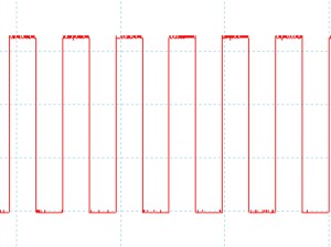
Clock Signal

Compiling and deploying this code to the processor results in the following output on pin 3 of port D:

One millisecond clock signal on port D, pin 3.

The scope we set up for 2 milliseconds per division and this looks about right. The exact frequency count comes out to be 976.6 Hz which is right if you divide the clock signal by the prescaler.

Connecting up the STM8S003

Sunday, April 29th, 2012

A few days ago I wrote about my first attempt at coding for the STM8S003 but forgot to mention how I connected up the chip to the PC. So here is a quick post explaining how to do it.

The STM8S Chip

The STM8S chip chosen was the STM8S003F3 in a TSSOP20 package. This form factor is incredibly small and there is no way to mount it on a breadboard without some for of adapter. Luckily Sparkfun have a SSOP to DIP Adapter 20-Pin in their catalog. However, I could not get hold of one in the UK so I ended up getting the 28 pin version instead. A bit of a waste but it worked.

So armed with the adapter, a chip and some connectors it was time to break out the soldering iron. A brief experiment with drag soldering did not work and I finally settled on soldering each pin very carefully with the finest soldering iron tip I had.

STM8S on SSOP to DIP Adapter

The next job was to mount all of this on the breadboard. There are only really two additional components required for this circuit, 1uF and 0.1uf ceramic capacitors. You can see both of these to the left of the chip in the above picture. The 0.1uf capacitor connects ground and +3.3V and acts as a power smoothing capacitor. The 1uF capacitor connects Vcap and ground.

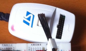
ST-Link/V2 Programmer and Debugger

The chip is programmed using the low cost (£20 approx) ST-Link/V2 programmer and debugger. This works with both the STM8 and STM32 range of processors.

ST-Link/V2 Programmer Debugger

Putting it all Together

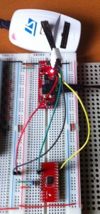
If we put the two components together we get something which looks like this:

STM8S On Breadboard

The red PCB between the programmer and the STM8S circuit is a breadboard power supply which has been set to supply 3.3C to the circuit. The wires connecting the STM8 to the programmer are as follows:

Colour Description
Red Power (3.3V)
Black Ground
Green Reset
Yellow Data

Netduino Go! Module Development – the First Steps

Friday, April 27th, 2012

The last few weeks I’ve been getting things together to start to look at developing a smart module for the Netduino GO!. This post looks at the first steps and ends up with some working code on a STM8S003 chip.

STM8S Discovery

My starting point was to get the software tools installed and working. In order to verify this I purchased the STM8S Discovery board. This has the STLink module and a STM8S105 microcontroller built into a convenient package for less than £7.00. This board itself was easy to set up and worked straight out of the box.

Development Environment

Having the board is one thing but we need a development environment to work with. I tried several environments and in the end I found I was happiest with the IAR environment so for the moment I’m sticking with it whilst I find my feet. Set up was easy and it found the STM8S Discovery straight away.

Start With Something Simple

I wanted to start with a really simple project which would not require any additional hardware other than a scope to check that the application was working. That way I could transfer the program to a microcontroller on a breadboard and know that I had as few possible points of failure as possible. To this end I decided that I would put the microcontroller clock pulses out on one of the pins. I could verify that everything was working but uploading a new program which changed the clock scaler and if all was well I would see a different trace on the scope.

This choice of application was no accident as the data sheet for the chip shows that it has a pin labelled CCO. You can configure this pin to output the controller’s clock signal. Not only that but you can also use the microcontroller’s internal clock generator as the clock signal. So in theory, all I needed to do was add a few discrete components to the breadboard along with the STM8S and I should have a small, simple, self contained system to test the tool set.

Creating a New Project

First thing to do is create a new workspace and project using IAR. Simple enough, enter a name for both and a new main.c is presented to you. Good game but not much use as it stands.

Luckily ST provide a standard library of drivers for the various features available on their chip sets. I downloaded version 2.1.0 of the library and this contained the drivers and some sample applications. The trick is to understand the way in which you access the libraries. It’s really simple and basic. In effect, you add the C source files for the library to your application and compile your application and the libraries at the same time. Both of these are then deployed as a single binary to the microcontroller. Basic but it works. The source files are broken down by microcontroller feature. So, all of the routines etc. for timer 2 are in the header file stm8s_tim2.h and the source code is in the file stm8s_tim2.c.

To make things easier (well, easier for me anyway) I have taken to copying the source and include files from the standard library provided into each project directory I create. That way you simply need to add the source file for a feature as you need it. In this case the only feature I’m going to be using is the clock and so I need to make sure I add the stm8s_clk.c file to the project.

The stm8s.h file contains definitions for a whole range of controllers. It is therefore necessary to define a preprocessor macro for the type of controller the application is targeting. This can be done in one of two ways, either in the stm8s.h file itself (as this in included in the other standard library files) or as a macro in the project. I personally prefer to do this in the project as it makes updating the library code easier.

So Let’s Get Started

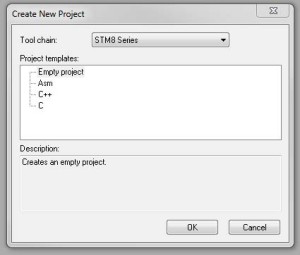
First thing to do is to get a workspace and project created. So open IAR and create a new workspace. Next, go to the Project Menu and create a new project. The following dialog should appear:

New Project Dialog

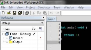
Select a C project and click OK. The next dialog asks you to select a name and location for the project. So decide on a location and name. Being very creative, I went for Test as the project name. Once completed I had a project which looked like this:

New C Project.

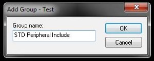
The next job is to add the include and source files for the standard peripheral library. So copy the include and source files from the library and add them to the directory containing your project. I normally put the include files in the inc directory and the sources in the src directory. The next thing to do is add these files to the project. So right click on the project name (in this case Test – Debug and select Add – Add Group. Enter the name STD Peripheral Include

Add new file group

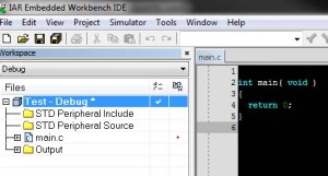
Repeat this to add the source file group with the name STD Peripheral Source. Your project should now look like this:

File Groups Added to Project

Now we need to add the files to the groups. For the include files I add all of the files. For the source files I only add the ones I will be using. To do this you right click on one of the file groups we have created, say the STD Peripheral Include group and select Add – Add Files…. For the include files navigate to the directory containing the copied files and select them all.

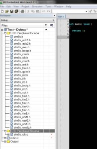
Repeat for the source files but this time we only select the files we will be using. In this case the clock file stm8s_clk.c. Your project should now look something like this:

All Files added

There are still a few extra steps before we can write some code. The STM8S include files require that the type of chip is defined before any code will compile so we will need to define a preprocessor macro indicating which chip we are using. Next we need to tell the compiler about the location of the include files. Finally, we need to tell the system how to deploy and debug the application.

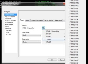
So let’s start off with the chip family. Firstly we want to tell the compiler about the target family. So right click on the project name and this time select Options. Under General options, select the chip family to be targeted. For the Discovery board the family is STM8S105, for the final module we will be targeting the STM8S003.

Select chip family.

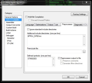
The next step is to tell the preprocessor about the chip family and the location of the include files. From the same dialog as above, select the C/C++ compiler and the Preprocessor tab. Add the entry $PROJ_DIR$inc to the include files and define a symbol for the chip set. Define STM8S105 for the Discovery board and STM8S003 for the final module.

Pre-processor Options

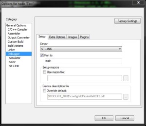
The final step is to tell the IDE how to deploy and debug the application. From the Options dialog select the Debugger category and set the Driver to ST-LINK.

Debugger Options.

Now click on OK to set the options. We can now start to write some code.

Let’s Write Some Code

Replace the code in the main.c file with the following:

#include "stm8s.h"
#include "stm8s_clk.h"

int main(void)
{
    CLK_DeInit();
    CLK_SYSCLKConfig(CLK_PRESCALER_CPUDIV1);                // CPU Prescaler = 1.
    CLK_SYSCLKConfig(CLK_PRESCALER_HSIDIV8);                // Prescaler = 8, 2 MHz.
    CLK_CCOConfig(CLK_OUTPUT_HSI);                          // Output clock on CCO pin.
    CLK_ClockSwitchConfig(CLK_SWITCHMODE_AUTO,              // Automatically switch
                          CLK_SOURCE_HSE,                   // Switch to internal timer.
                          DISABLE,                          // Disable the clock switch interrupt.
                          CLK_CURRENTCLOCKSTATE_DISABLE);   // Disable the previous clock.
}

Connect up board/chip and hit Ctrl-D. This will compile and deploy the application. The debugger should start with the first line of main highlighted. Press F5 and the application should start. Hooking up the oscilloscope gave the following trace:

Oscilloscope Output

The clock frequency of the chip using the internal high speed oscillator is 16 MHz. Diving this by 8 should give a 2 MHz signal (as indeed the above trace shows). Just to check if this is a coincidence, change to CLK_PRESCALER_HSIDIV8 to say CLK_PRESCALER_HSIDIV4 and the scope output should change to show the new clock frequency and sure enough it does.