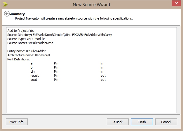
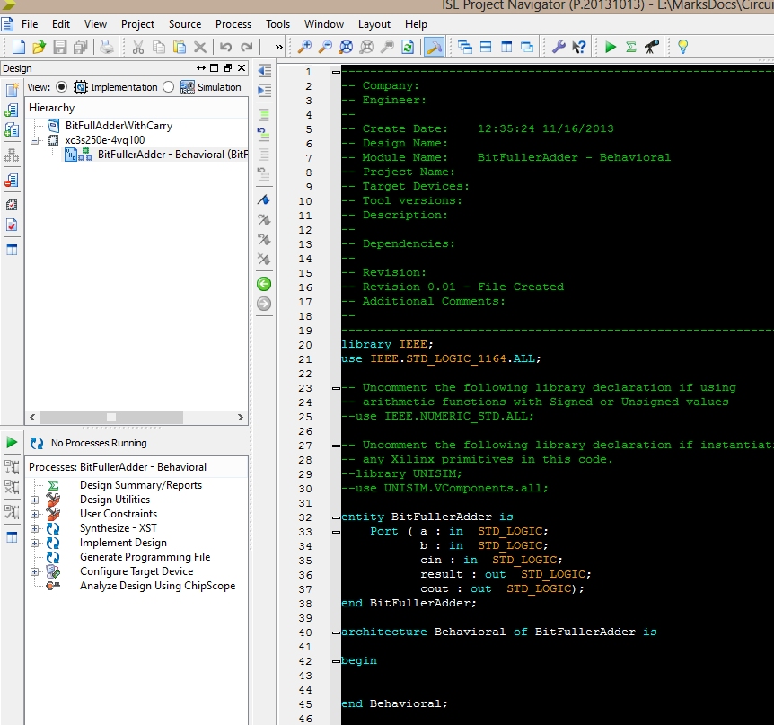
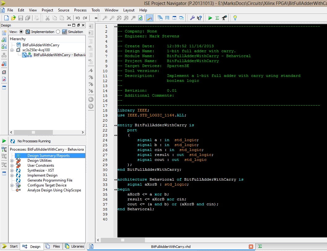
Clocks, Reset Signals and Switch Debouncing
February 16th, 2014 • Electronics, Home Built CPU, MSP430 • Comments Off on Clocks, Reset Signals and Switch DebouncingEvery computer needs a clock circuit to synchronise the operation of the various components. A CPU is no exception. In this post we will create a clock for the CPU. We will also add reset and single step circuits.
The brief for this post is as follows:
- The reset circuit must be capable of generating both high and low reset signals.
- A stop/run circuit should allow the CPU to be stopped by the user and the clock single stepped.
- Internal clock source with a master clock of 4 MHz.
- Selectable clock frequency which is a fraction (half, quarter etc.) of the master clock source.
Reset Signals
The requirement to have both high and low reset signals is not really too complex as a single inverter can provide this capability. The most complex part of this requirement is to remove the switch bounce from the signal.
Switch De-bouncing
For new readers, switch bounce occurs due to the imperfect nature of mechanical switch. For a brief period of time when a switch is depressed or released there will be a period where the electrical signal is not stable. If you connect an oscilloscope to a switch in an electrical circuit and press the switch you are likely to see traces such as the following:
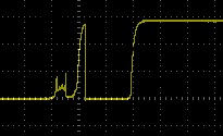
Switch Bounce
The obvious outcome of this is that the circuit can act as though the switch has been pressed multiple times in a short period of time. The answer to the problem is to de-bounce the switch. This removes the additional signals which can be generated. For microcontroller developers there are two possible solutions to this problem, software or hardware de-bouncing. As we have no conventional software environment available to us we must achieve this by hardware de-bouncing.
There are many possible solutions to this problem and you can find some discussions in the following links:
- Lab Book Pages
- University of Utah Engineering
In this circuit there are two switches to debounce, the reset switch and the clock selection switch. The reset switch is a momentary switch and the clock selection switch is a rotary switch. The rotary switch should be viewed as a momentary switch for the purposes of this exercise.
The problem of debouncing the switch can be broken down into two distinct components, namely removing the jitter by rounding off the signal and the squaring off the rounded signal. The jitter can be rounded off by the use of a RC circuit. The above articles suggest that the rounded signal can be squared using an inverter with a Schmitt trigger.
Time to break out the breadboard, oscilloscope and the calculator.
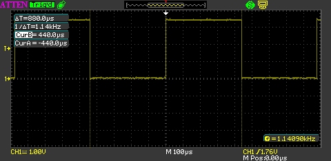
The first thing to examine is the amount of bounce for the switches being used. Hooking up the momentary switch and a resistor resulted in the following traces for the depression of the switch:
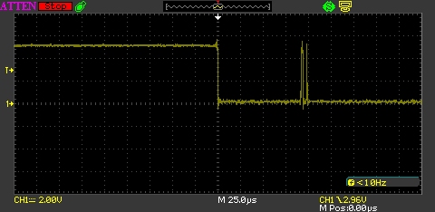
Switch Bounce Depression
And for the release of the switch:
Switch Bounce Release
Taking some measurements we see that the maximum bounce appears to be about 5ms for the momentary switch.
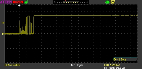
Repeating the exercise for the rotary switch reveals that this switch was a lot dirtier. The bouncing continued for about 10ms in the worst case.
Taking the worst case scenario we should assume that the switch is unstable for 10ms and 20ms would allow for an extreme case.
There are two possibilities for debouncing, hardware and software. For a large commercial run where a microcontroller is in use then software debouncing would be used as it requires no additional components. As this is a small run, hardware debouncing is a possibility.
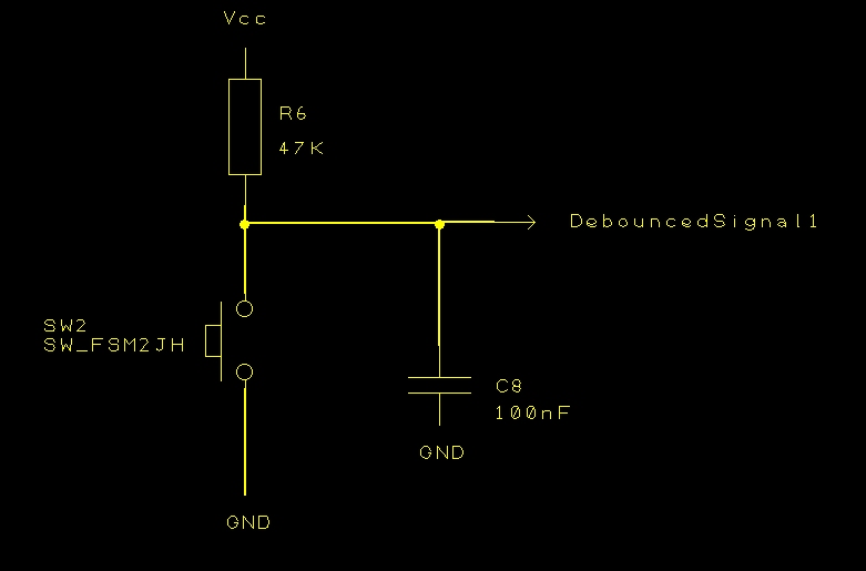
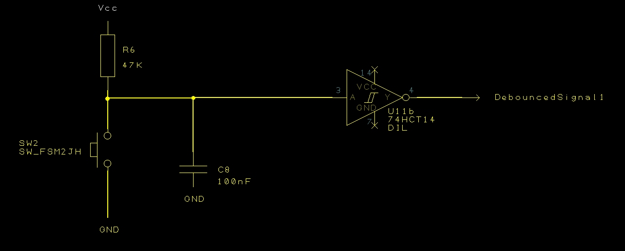
Hardware Debouncing (Circuit 1)
This first hardware debouncer will use an RC network connected to a Schmitt triggered inverter. The basic circuit is:
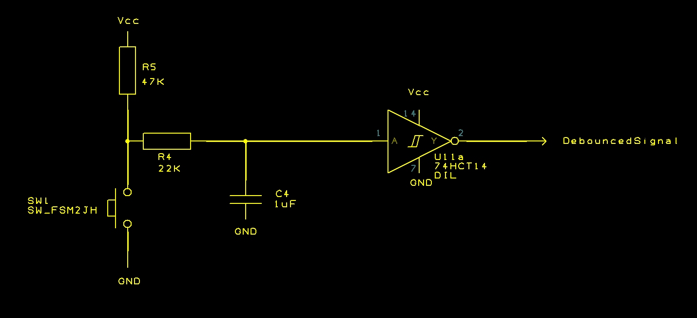
2RC Debounce
The capacitor C4 charges through R4 and R5. When the capacitor is charged the input to the inverter is high and the output will be low.
Depressing the switch starts the discharge cycle for the capacitor. The capacitor slowly discharges through R4 until it is below the level associated with logic 0 on the inverter. The output of the inverter then goes to logic level 1. The hysteresis of the inverter makes the gate resistant to the time the voltage applied to the input of the inverter is between logic 1 and logic 0. So pressing the switch takes the output high and releasing the switch takes the output from the circuit low.
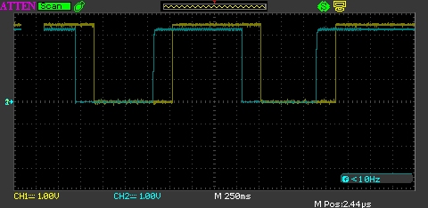
The trick with the circuit above is to select values for R4, R5 and C which eliminate the bounce at both the charge and discharge points in the circuits operation. This circuit gives an output something similar to the following:
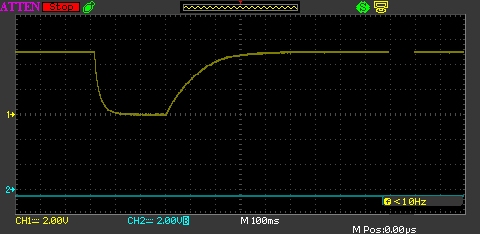
RC Added to Switch
The yellow trace shows the output of the circuit when the oscilloscope probe is connected to the input of the inverter. As you can see, the noisy signal has been replaced by a rapid decay at the start (when the switch is depressed) and a longer rise at the end when the switch is released.
Hardware Debouncing (Circuit 2)
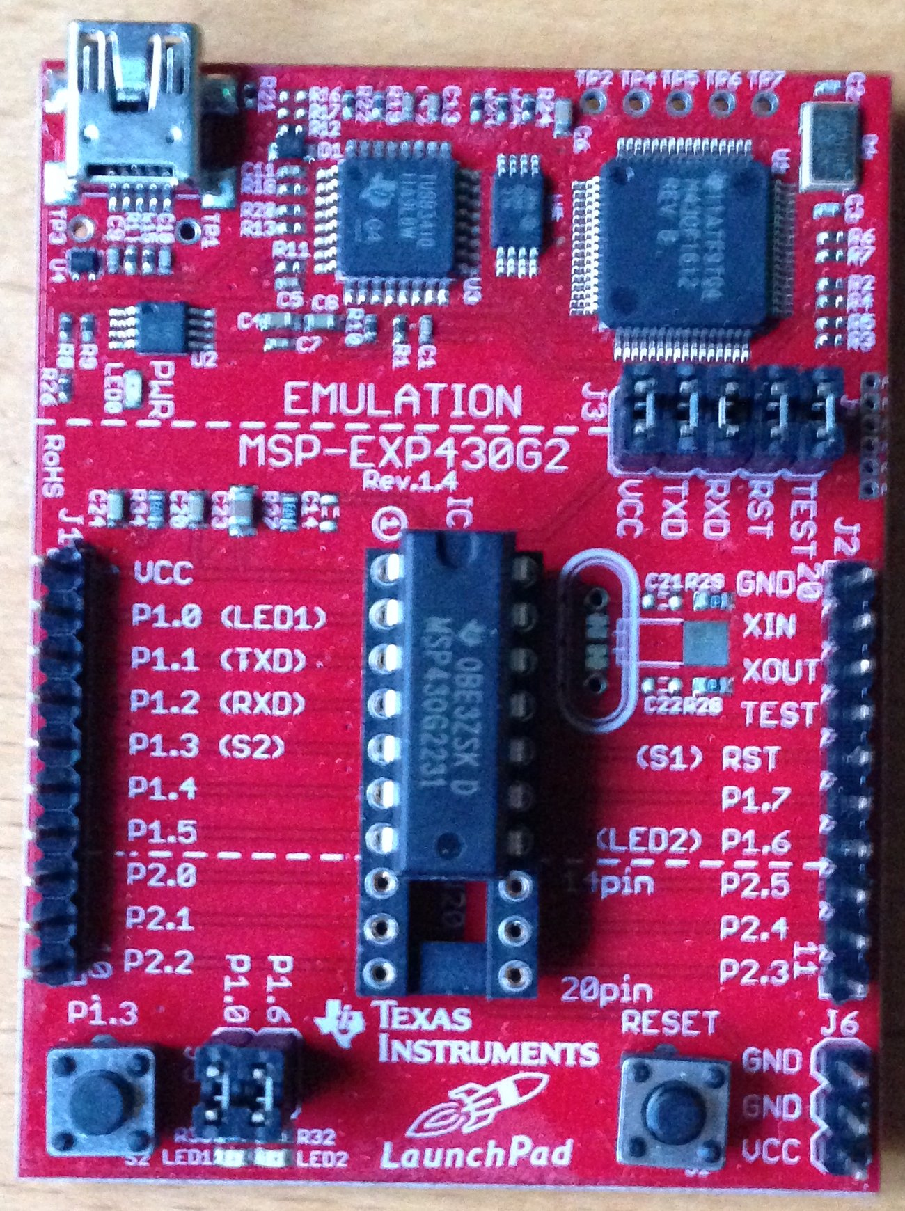
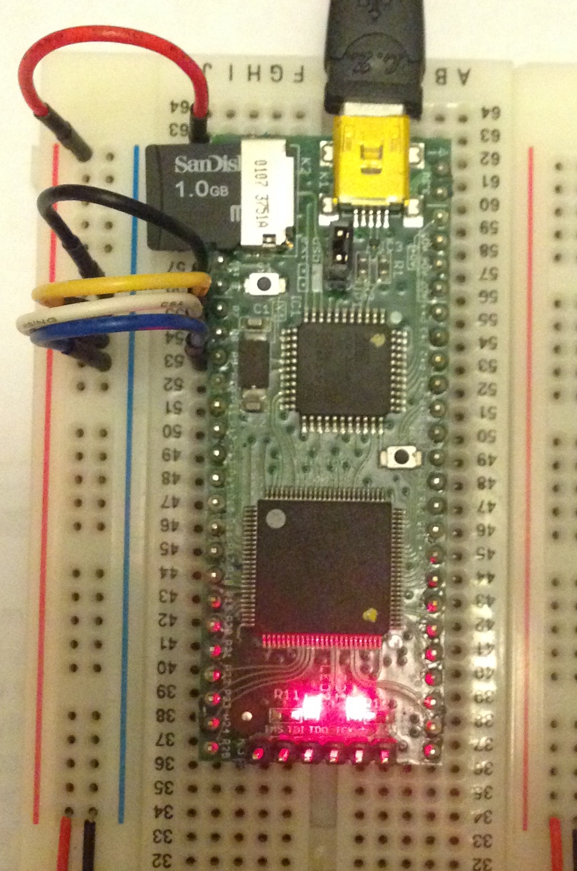
In the last post I was looking at the MSP430. The intention is to look at how it can be used for software debouncing (we’ll come on to that later). The MSP430 Launchpad has a reset button connected to Port 1, pin 3 (P1.3) and this switch is also debounced (the schematics are freely available from TI’s web site). The debounce circuit on the MSP430 looks something like this:
MSP430 Launchpad Debounce Circuit
Modifying this to add an inverter we get the following:
Modified MSP430 Debounce Circuit
The discharge when the button is pressed is a lot quicker but the charging when the button is released show the same characteristics as Hardware Debouncing (Circuit 1). Examining the trace we see that the output from the inverter is good enough for the job at hand.
Software Debouncing
The algorithm for software debouncing is relatively trivial. The microcontroller waits and detects the changing input on of the the pins (say going low to high). Once detected, start a timer and wait for the worst case scenario (we set this to 20ms for the switches being used in this circuit). If at the end of the time period the signal is still high then set the output high, otherwise start the whole process again.
Now this algorithm works well for a single input to a microcontroller but what if you have multiple inputs and outputs all of which need debouncing. This is the scenario with this circuit as the rotary switch allows one selection to be made from a multiple of inputs. In this case the rotary switch acts like multiple switches. Following the above algorithm would require multiple interrupts and timers, many more than found on low end microcontrollers.
Modifying the algorithm to use timers and counters can solve this problem.
- Initialise an array of counters (one for each input) to 0
- Set the outputs to the same level as the inputs
- Setup a timer to trigger on a regular period (say 8ms)
- For each input, if the input is different to the output increment the counter for that input, otherwise set the counter to 0
- For each counter, if the value has exceeded the threshold count then set the output to the same level as the input
Although this is a little more convoluted it does allow switch debouncing for multiple switches with a simple and cheap microcontroller.
Software Debouncing on the MSP430
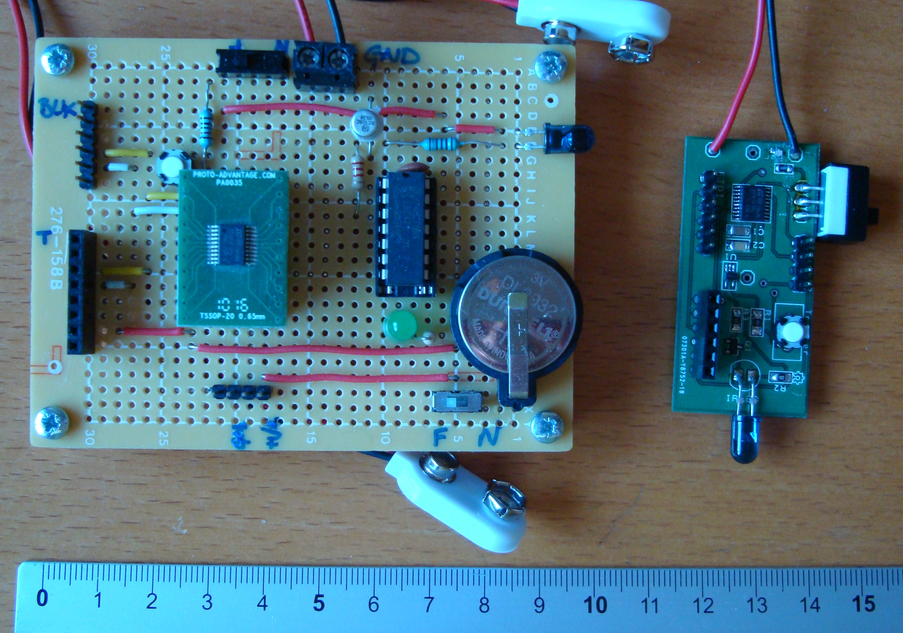
The software debouncer will be implemented in MSP430 assembler code developed using IAR Embedded Workbench.
The first thing we need is somewhere to store the counters and some workspace for the application. This application is small and so the registers on the chip should suffice.
;--------------------------------------------------------------------------------------------------
;
;   Switch debouncer for the home made CPU.  This will debounce five switches
;   four through Port 1 and 1 through port 2.
;
;   Copyright (c) Mark Stevens 2014
;
;--------------------------------------------------------------------------------------------------
#include <msp430.h>

;--------------------------------------------------------------------------------------------------
;
;   Global definitions
;
;--------------------------------------------------------------------------------------------------
;
;   Define some symbolic names for the registers holding the counts of the number of interrupts
;   for which the value on the input differs from the output.
;
#define  port0Count r4
#define  port1Count r5
#define  port2Count r6
#define  port3Count r7
;
;   Now some temporary workspace for the Watchdog ISR.
;
#define inputRegister r9
#define temporaryRegister r10
;
INTERRUPT_BASE      equ     0xffe0                  ; Base address of the interrupt vector table.
MAX_COUNTS          equ     4                       ; 4 counts equates to 24ms.
The above defines some symbolic names for the counters and maps these names onto four registers. These are also two registers reserved for workspace for the application.
;--------------------------------------------------------------------------------------------------
;
;   Main program
;
;--------------------------------------------------------------------------------------------------
                    org     0xf800                          ; Program Reset
main                mov     #0x280, SP                      ; Initialize stackpointer
StopWDT             mov.w   #WDT_MDLY_8, &WDTCTL            ; WDT ~8ms interval timer
                    bis.b   #WDTIE, &IE1                    ; Enable WDT interrupt
                    ;
                    ;   Setup the counters.
                    ;
                    mov.w   #0, port0Count
                    mov.w   #0, port1Count
                    mov.w   #0, port2Count
                    mov.w   #0, port3Count
                    ;
                    ;   P1.0, 2, 4, 6 are inputs, P1.1, 3, 5, 7 are outputs.
                    ;
                    bis.b   #0xaa, &P1DIR
                    mov.b   &P1IN, &P1OUT                   ; Start with the outputs equal to the inputs.
                    ;
                    ;   Put the chip to sleep waiting for interupts.  Put it back to sleep
                    ;   if it ever wakes up.
                    ;
Mainloop            bis.w   #CPUOFF + GIE, SR               ; CPU off, enable interrupts
                    jmp     Mainloop
The main program initialises the counters and the ports and turns on the watchdog interrupt (triggered every 8ms – approx). The main program then puts the chip to sleep until the Watchdog interrupt fires.
;--------------------------------------------------------------------------------------------------
;
;   Watchdog interrupt
;
;   Check the input pins (0, 2, 4, 6) and if they are different to the output pins then increment
;   the counter for that pin.
;
;   If the counter reaches MAX_COUNT then transfer the input to the output.
;
;   If the input equals the output then set the counter to 0.
;
;--------------------------------------------------------------------------------------------------
WatchdogISR         mov.b   &P1IN, inputRegister
                    mov.b   &P1OUT, temporaryRegister
                    clrc
                    rrc     temporaryRegister
                    xor.b   temporaryRegister, inputRegister
                    and     #BIT0, inputRegister
                    jz      resetPort0Counter               ; Input bit and output bit are the same.
                    ;
                    ;   Now check the port counters
                    ;
                    inc     port0Count
                    cmp     #MAX_COUNTS, port0Count
                    jne     checkPort2                      ; Not enough differences.
                    ;
                    ;   Transfer the input to the output and reset the counter.
                    ;
                    bit.b   #BIT0, &P1IN
                    jz      resetPort0
                    bis.b   #BIT1, &P1OUT
                    jmp     resetPort0Counter
resetPort0          bic.b   #BIT1, &P1OUT
resetPort0Counter   mov.w   #0, port0Count
checkPort2          ;
                    ;   Checking the remaining ports is left as an exercise for later.
                    ;
                    reti
This is where calculations are performed. Note that the above code only works for one input pin but it can easily be extended to work with four pins. The first thing this routine does is to extract the input and output states of the port. It then works out if there is a difference between the input on P1.0 and the output on P1.1.
The middle block of code increments the counter and checks to see if the counter has reached the threshold. If it hasn’t then we move on to the next port.
The final block of code is executed if the port input/output are different. It transfers the input to the output and then resets the counter.
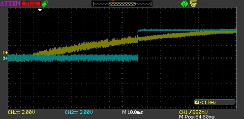
Deploying this code to the MSP430 and connecting a switch gave the following trace on the oscilloscope:
Switch With Delay
As you can see, there is a delay between the switch being depressed and the output being set. The blue trace is wired to the microcontroller input and the yellow trace is the output.
Selecting a debouncer
After many hours working on this circuit I have elected to go with Hardware Debouncing (Circuit 2) with the addition of the Schmitt inverter. This circuit is relatively simple and also meets my long term design goals for this project, namely to use only 1970/80’s technology and using logic gates where possible. It also removes the issue that the MSP430 has a maximum supply voltage of 3.6V and the remainder of this project will be working at 5V.
Selecting the Inverter
Throughout this design process I hit an issue with the inverters I have. I was trying to use the 74LS14 hex Schmitt inverter. For some reason this chip was outputting 1V on the input pin of the logic gate. I could not get the circuits above to work and in the end I ordered some 74HCT14 Schmitt Inverters. Voila, I now have a working debounce circuit.
Something to investigate later…
Reset Circuit
One possibility would be to use the output from the debounced reset switch as a reset signal. This would lead to a variable length reset pulse. Whilst an overly long reset pulse would not be an issue there may be problems if the pulse is too small. This can be solved by using an NE555 timer in monostable mode. The reset signal will still be variable but it will never be shorter than the defined by the components used to control the NE555.
The schematic for the basic monostable NE555 circuit looks as follows:
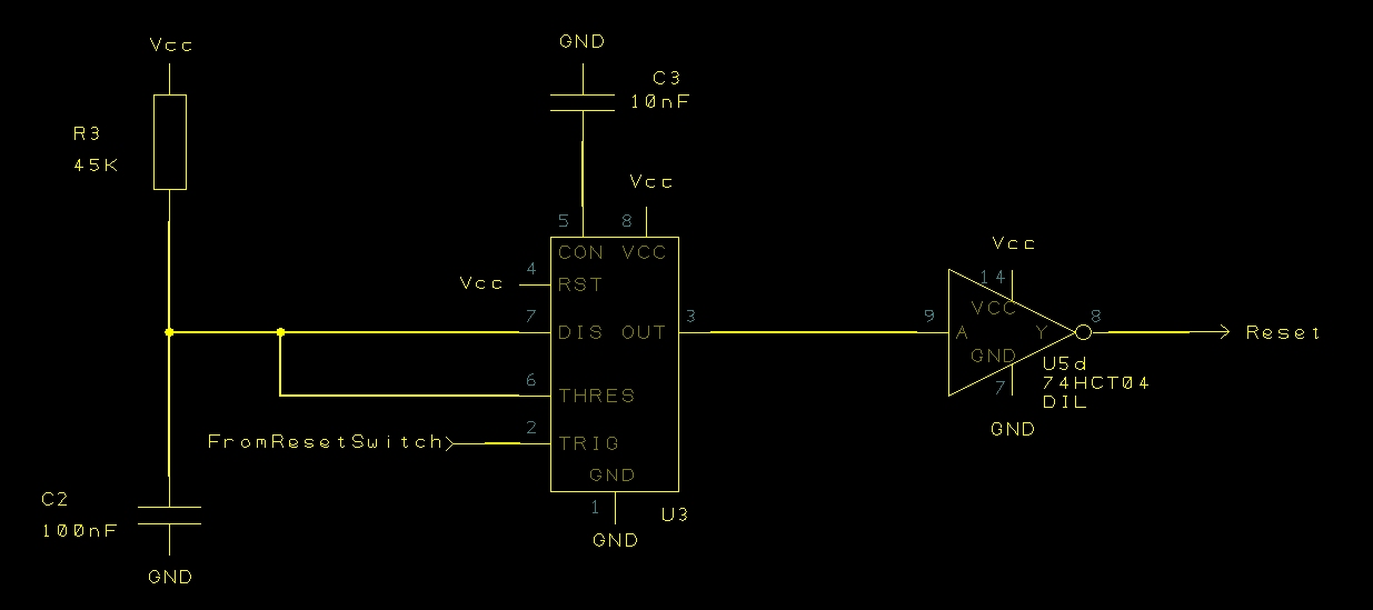
NE555 Reset Circuit
The length of the pulse is determined by the following formula:
t ~= 1.1RC
In our case R = R3 and C = C2. So this gives:
t ~= 1.1 * R3 * C2>
=> t ~= 1.1 * 45,000 * 100 * 10-9
=> t ~= 4.95ms
At 4.95ms this might be a little close to the 5ms bounce seen by some of the switches in use. Increasing the values of R3 and C = C2 will increase the duration of the reset pulse. Making R3 = 180K we see the following at the end of the signal:
NE555 End of Reset Signal
The full reset pulse looks like this:
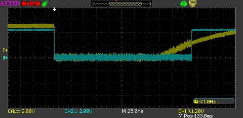
NE555 Full Reset Pulse
Clock Circuit
The clock for the project can be broken down into two parts:
Oscillator Circuit
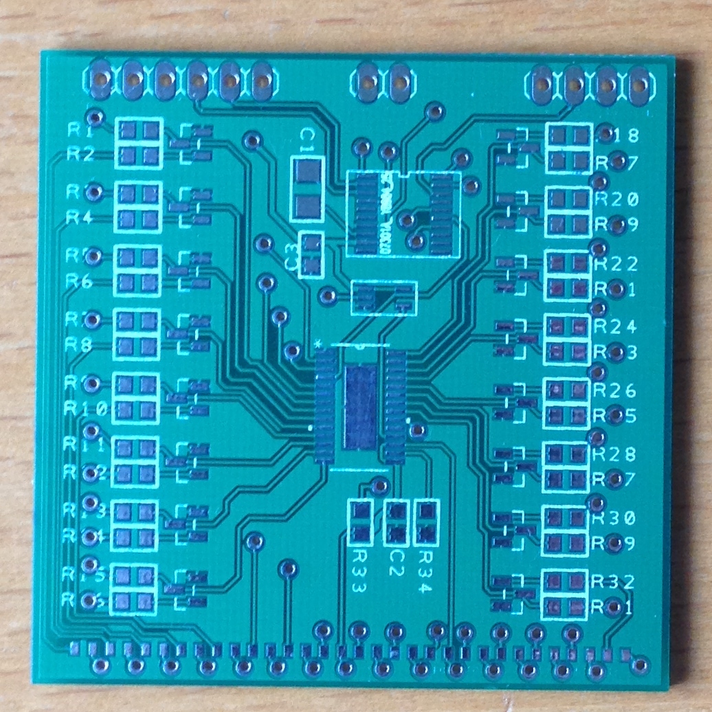
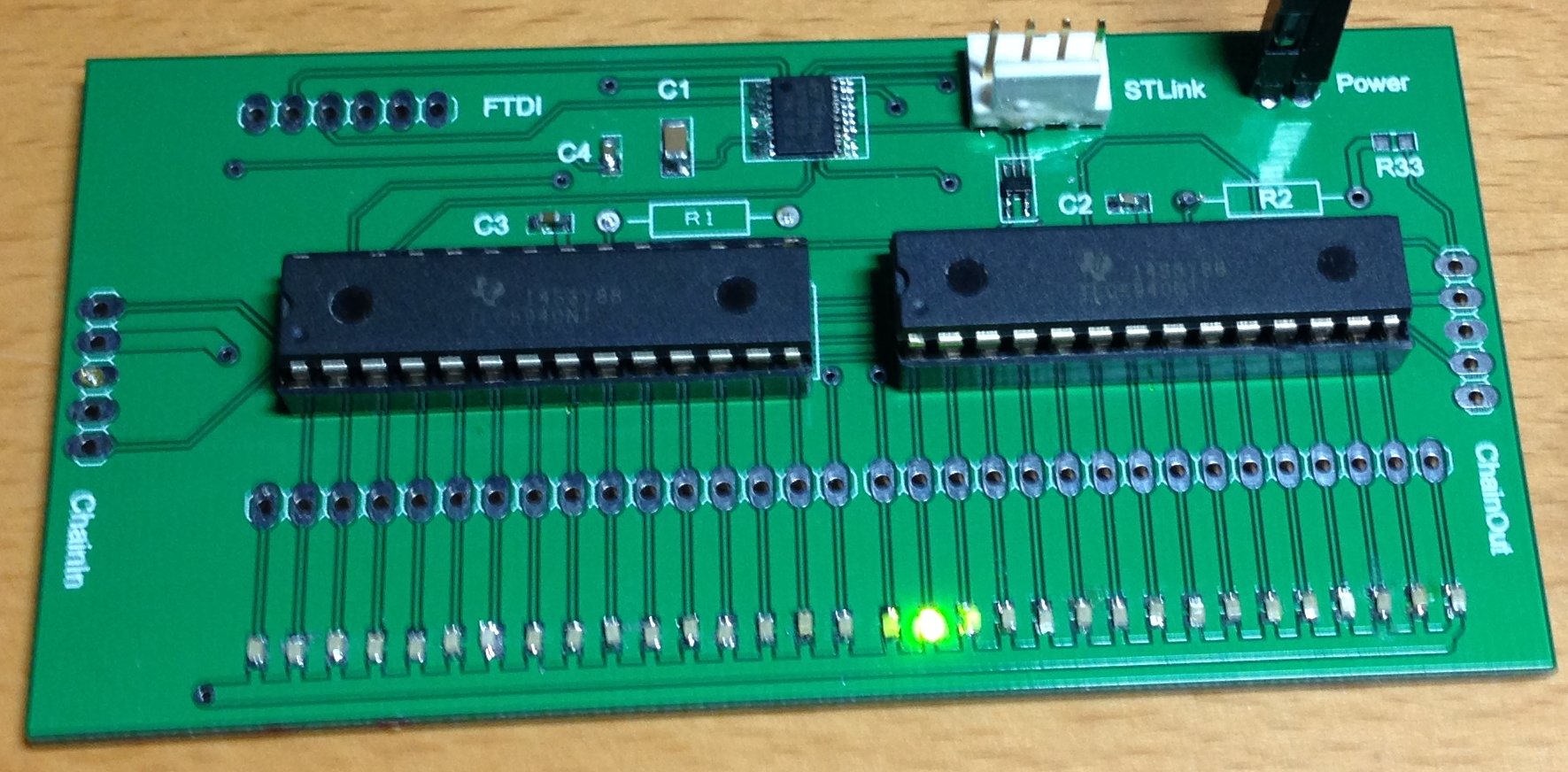
The oscillator circuit will provide the circuit with the “master clock”. These have been used previously on this blog in the TLC5940 circuit developed a few years ago. In the spirit of reusing old work where possible we will use the basic oscillator circuit from that post here. By changing the 8 MHz resonator for a 4 MHz part we should be able to achieve a 4 MHz master clock signal.
The schematic for the oscillator can be found below.
Dividing the Clock
Dividing the clock circuit by two is easy enough to achieve using a flip-flop. The basic logic diagram is as follows:
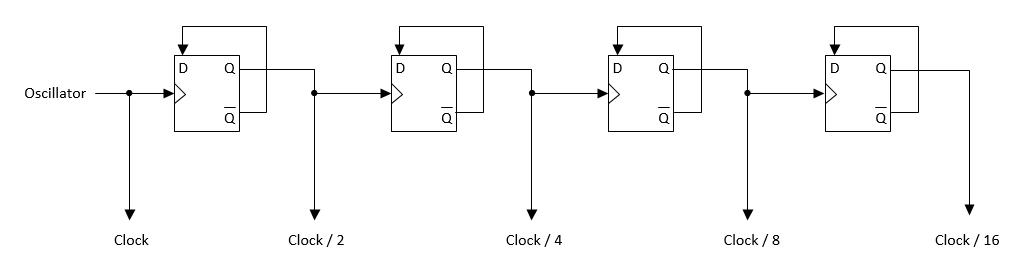
Flip-Flop Divider
Circuit courtesy of Electronics Tutorials.
This is easily implemented using the 7474 Dual D-Type Flip-Flops with Preset and Clear.
The selection of the clock should also be easy if we make the decision that it is invalid to change the clock frequency whilst the system is running. We will rely upon the user to have the discipline not to change the clock in run mode. Since this is an initial design we can look at changing it later.
This decision means that initially we do not have to worry about glitches due to the clock frequency being changed.
The selection of the clock frequency can be achieved by feeding all of the clocks into one input of a dual input AND gate. The second input to the gate can then be connected to a rotary switch. The switch will connect the second input to high for the selected frequency. All of the inputs to the other gates will then be grounded. This means that only one gate allows a clock signal through to the system clock signal output.
We can also use the debounce circuit described above to ensure a smooth transition from one clock to another.
The schematic for this looks like this:
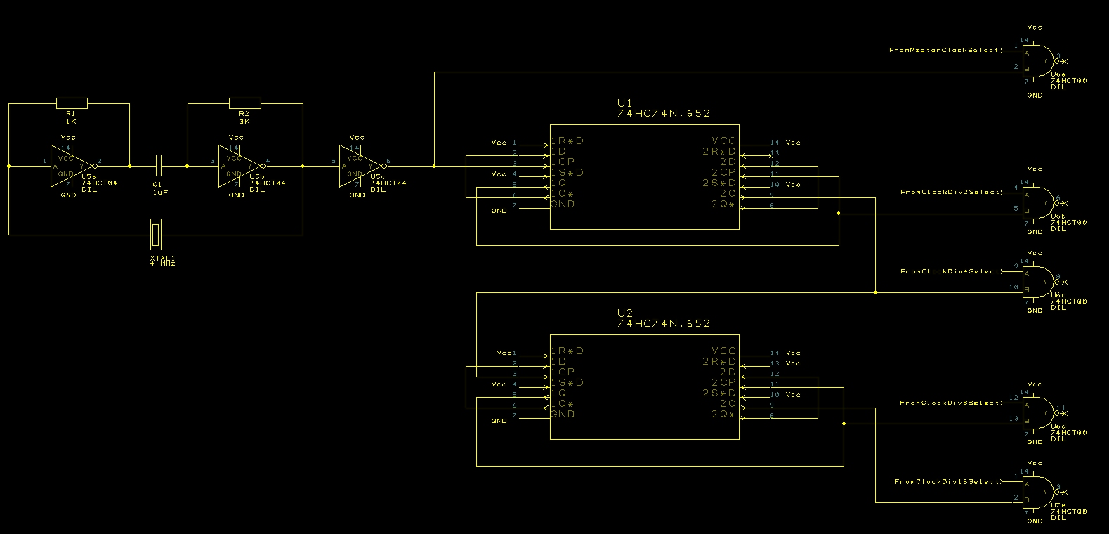
Oscillator and Clock Dividers
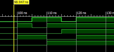
By hooking up the logic analyser to the system clock output and the various outputs from the clock divider circuit we see the following:

Clock and Flip Flop Output
Hooking up the rotary switch to the debounce circuit and the AND gates will allow the selection of the master clock output.
Conclusion
The home built CPU is on it’s way. We now have a heart beat (clock) for the circuit and a method for issuing a reset request to the circuit.
One final refinement would be the addition of a buffer driver chip to the circuit to allow for the fact that the clock and reset signals will be being fed into a larger circuit.