RSS

Archive for the ‘STM32’ Category

SPI and the STM32

Monday, March 17th, 2014

STM32 Discovery With Logic Probes

This post was supposed to be about controlling an LED panel using SPI on the STM32. It soon became apparent that SPI on the STM32 was a topic of it’s own and so the hardware component of the post, the LED panel, will have to wait for another day.

In this post we will aim to achieve the following:

  1. Use SysTick to trigger regular events
  2. Send data over SPI by polling
  3. Use interrupts to send data by SPI
  4. Combine SPI and DMA to send data over SPI

So let’s start with the trigger/heartbeat.

Heartbeat

The heartbeat will allow us to perform tasks at regular intervals, say 1ms, and by toggling a pin we can also determine if the processor is still “alive”.

For a simple heartbeat we can use the SysTick timer. This built in timer can be configured to generate an interrupt. The handler has it’s own entry in the interrupt vector table. It is theoretically possible to calibrate this timer to trigger at an accurate period. For the purpose of this problem we will not really need high accuracy and so will simply turn on the timer.

Setting this timer running requires only two lines of code, encapsulating this into an initialisation method gives us the following:

//
//    Initialise SysTick.
//
void InitialiseSysTick()
{
    RCC_ClocksTypeDef RCC_Clocks;
    //
    //    Setup the system tick for the heartbeat.
    //
    RCC_GetClocksFreq(&RCC_Clocks);
    SysTick_Config(RCC_Clocks.HCLK_Frequency / 1000);
}

The SysTick_Config method sets up the SysTick timer. The timer works by loading the counter with a Load value. The counter then starts to count down from the load value each tick of the clock. When the counter reaches zero it is reloaded and the whole process starts again. It is possible to generate an interrupt (SysTick_Handler) when the counter reaches zero.

The expression RCC_Clocks.HCLK_Frequency / 1000 is the counter reload value. It is important to note that the reload value is a 24-bit unsigned long and so this has a maximum value of 0xffffff. In this case the load value is 0x29040, well within the specified range. This value will give 1000 interrupts per second, i.e. an interrupt every 1ms.

Now we have a 1ms interrupt we need to determine if this interrupt is being triggered. The simplest way of doing this is to toggle one of the GPIO pins. First thing to do is to select a pin and then initialise the port. Selecting PA1 we can modify the InitialiseSysTick code above to the following:

//
//    Initialise SysTick.
//
void InitialiseSysTick()
{
    GPIO_InitTypeDef GPIO_InitStructure;
    RCC_ClocksTypeDef RCC_Clocks;
    //
    //  Initialise the peripheral clock.
    //
    RCC_AHB1PeriphClockCmd(RCC_AHB1Periph_GPIOA, ENABLE);
    //
    //  Initialise the heartbeat GPIO port.
    //
    GPIO_InitStructure.GPIO_Pin = GPIO_Pin_1;
    GPIO_InitStructure.GPIO_Mode = GPIO_Mode_OUT;
    GPIO_InitStructure.GPIO_OType = GPIO_OType_PP;
    GPIO_InitStructure.GPIO_Speed = GPIO_Speed_50MHz;
    GPIO_InitStructure.GPIO_PuPd = GPIO_PuPd_NOPULL;
    GPIO_Init(GPIOA, &GPIO_InitStructure);
    //
    //    Setup the system tick for the heartbeat.
    //
    RCC_GetClocksFreq(&RCC_Clocks);
    SysTick_Config(RCC_Clocks.HCLK_Frequency / 1000);
}

The next task is to add the SysTick interrupt handler. Opening the startup_stm32f4xx.c file you will find the following line:

#pragma weak SysTick_Handler = Default_Handler

This statement defines the SysTick_Handler and points the handler to the Default_Handler. The weak attribute allows the developer to override this handler and provide their own interrupt handler. In our case we want the handler to toggle PA1. This gives the following code:

//
//    System tick handler.
//
void SysTick_Handler(void)
{
    //
    //    Generate a heartbeat.
    //
    GPIOA->ODR ^= GPIO_Pin_1;
}

All of the above code is placed in a file SysTick.c and an appropriate header file created. Our main program file is:

#include "SysTick.h"

//
//    Initialise the system.
//
void Initialise()
{
    InitialiseSysTick();
}

//
//    Main program loop.
//
int main()
{
    Initialise();
    while (1);
}

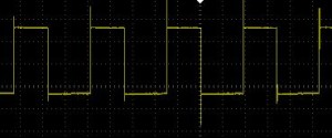
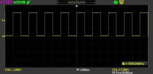
Putting this into a project, compiling and running results in the following output on the oscilloscope:

500Hz Square Wave

500Hz Square Wave

As you can see, we have a 500Hz square wave indicating that PA1 is being toggled 1,000 times per second.

Polled SPI

Polled SPI will use the various registers associated with the SPI feature to determine if the SPI data transmission has completed. You can also use interrupts, a subject we will come to later.

The first things we need to do is to configure the pins required to support SPI. For conventional SPI we need four pins:

  1. MOSI (PA7)
  2. MISO (PA6)
  3. SCLK (PA5)
  4. Chip select (PE6)

One change we will make is to move the heartbeat from Port A to Port E (PE5) and keep Port A for the SPI function. Abstracting the GPIO initialisation out to it’s own files gives the following header file:

//
//    Include file for the GPIO methods.
//
//    Copyright 2014 Mark Stevens
//
#include "stm32f4xx_rcc.h"
#include <stm32f4xx_gpio.h>


#ifndef _SPI_H_
#define _SPI_H_

#ifdef __cplusplus
extern "C"
{
#endif

void InitialiseGPIO();

#ifdef __cplusplus
}
#endif

#endif

and the code file:

//
//    GPIO methods.
//
//    Copyright 2014 Mark Stevens
//
#include "GPIO.h"

//
//    Initialise the GPIO ports setting up the clocks.
//
void InitialiseGPIO()
{
    GPIO_InitTypeDef GPIO_InitStructure;
    //
    //  Initialise the peripheral clocks.
    //
    RCC_AHB1PeriphClockCmd(RCC_AHB1Periph_GPIOA, ENABLE);
    RCC_AHB1PeriphClockCmd(RCC_AHB1Periph_GPIOE, ENABLE);
    //
    //    Configure pins used by SPI1:
    //        PA5 = SCLK
    //        PA6 = MISO
    //        PA7 = MOSI
    //
    GPIO_InitStructure.GPIO_Pin = GPIO_Pin_7 | GPIO_Pin_6 | GPIO_Pin_5;
    GPIO_InitStructure.GPIO_Mode = GPIO_Mode_AF;
    GPIO_InitStructure.GPIO_OType = GPIO_OType_PP;
    GPIO_InitStructure.GPIO_Speed = GPIO_Speed_50MHz;
    GPIO_InitStructure.GPIO_PuPd = GPIO_PuPd_NOPULL;
    GPIO_Init(GPIOA, &GPIO_InitStructure);
    //
    //    Configure the Port E:
    //        PE6 - SPI chip select pin.
    //        PE5 - 1ms heartbeat.
    //
    GPIO_InitStructure.GPIO_Pin = GPIO_Pin_6 | GPIO_Pin_5;
    GPIO_InitStructure.GPIO_Mode = GPIO_Mode_OUT;
    GPIO_InitStructure.GPIO_OType = GPIO_OType_PP;
    GPIO_InitStructure.GPIO_Speed = GPIO_Speed_50MHz;
    GPIO_InitStructure.GPIO_PuPd = GPIO_PuPd_UP;
    GPIO_Init(GPIOE, &GPIO_InitStructure);
}

Calling the InitialiseGPIO method sets up Port A for SPI and Port E for general IO.

The next step is to initialise the SPI port:

  • Clock is idle low
  • Data is sampled on the rising edge
  • SPI Master
  • 8 data bits
  • MSB transmitted first
  • Clock prescalar 256 (slowest clock possible)

Coding this into an initialisation method gives:

//
//    SPI methods.
//
//    Copyright 2014 Mark Stevens
//
#include "spi.h"

//
//    Initialise SPI
//
void InitialiseSPI(void)
{
    SPI_InitTypeDef SPI_InitStruct;
    //
    //     Connect SPI1 pins to SPI alternate function.
    //
    GPIO_PinAFConfig(GPIOA, GPIO_PinSource5, GPIO_AF_SPI1);
    GPIO_PinAFConfig(GPIOA, GPIO_PinSource6, GPIO_AF_SPI1);
    GPIO_PinAFConfig(GPIOA, GPIO_PinSource7, GPIO_AF_SPI1);
    //
    //    Set PE6 high as we will be using active low for the
    //    device select.
    //
    GPIOE->BSRRL |= GPIO_Pin_6;
    //
    //     Enable the SPI peripheral clock.
    //
    RCC_APB2PeriphClockCmd(RCC_APB2Periph_SPI1, ENABLE);

    //
    //    Configure SPI1 in Mode 0:
    //        CPOL = 0 --> clock is low when idle
    //        CPHA = 0 --> data is sampled at the first edge
    //
    //    SPI Master mode, 8 bits of data, clock prescalar is 256, MSB is
    //    transmitted first.
    //
    SPI_InitStruct.SPI_Direction = SPI_Direction_2Lines_FullDuplex;
    SPI_InitStruct.SPI_Mode = SPI_Mode_Master;
    SPI_InitStruct.SPI_DataSize = SPI_DataSize_8b;
    SPI_InitStruct.SPI_CPOL = SPI_CPOL_Low;
    SPI_InitStruct.SPI_CPHA = SPI_CPHA_1Edge;
    SPI_InitStruct.SPI_NSS = SPI_NSS_Soft | SPI_NSSInternalSoft_Set;
    SPI_InitStruct.SPI_BaudRatePrescaler = SPI_BaudRatePrescaler_256;
    SPI_InitStruct.SPI_FirstBit = SPI_FirstBit_MSB;
    SPI_Init(SPI1, &SPI_InitStruct);
    //
    //    Enable SPI.
    //
    SPI_Cmd(SPI1, ENABLE);
}

As already noted, this first version of the SPI method will poll the SPI registers in order to determine the state of the SPI bus. The general algorithm is:

  1. Set the data register to the byte to be transmitted
  2. Wait for data transmission on MOSI to complete
  3. Wait for data reception on MISO to complete
  4. Wait until SPI is no longer busy
  5. Transfer the received data from the data register

Translating to C gives the following method:

//
//    Transmit and receive a single byte of data.
//
uint8_t SPISend(uint8_t data)
{
    //
    //    Setting the Data Register (DR) transmits the byte of data on MOSI.
    //
    SPI1->DR = data;
    //
    //    Wait until the data has been transmitted.
    //
    while (!(SPI1->SR & SPI_I2S_FLAG_TXE));
    //
    //    Wait for any data on MISO pin to be received.
    //
    while (!(SPI1->SR & SPI_I2S_FLAG_RXNE));
    //
    //    All data transmitted/received but SPI may be busy so wait until done.
    //
    while (SPI1->SR & SPI_I2S_FLAG_BSY);
    //
    //    Return the data received on MISO pin.
    //
    return(SPI1->DR);
}

And a header file for these methods:

//
//    Include file for the SPI methods.
//
//    Copyright 2014 Mark Stevens
//
#include <stm32f4xx.h>
#include <stm32f4xx_spi.h>
#include <stm32f4xx_gpio.h>
#include <stm32f4xx_rcc.h>

#ifndef _SPI_H_
#define _SPI_H_

#ifdef __cplusplus
extern "C"
{
#endif

void InitialiseSPI();
uint8_t SPISend(uint8_t);

#ifdef __cplusplus
}
#endif

#endif

Before we move on to the main program we need to remember to change the SysTick_Handler and initialisation method to take into consideration the changes we have made to the initialisation of the GPIO ports and the movement of the heartbeat to Port E. The SysTick.c becomes:

//
//    SysTick methods.
//
//    Copyright 2014 Mark Stevens
//
#include "stm32f4xx_rcc.h"
#include "stm32f4xx_gpio.h"
#include "system_stm32f4xx.h"

//
//    Initialise SysTick.
//
void InitialiseSysTick()
{
    RCC_ClocksTypeDef RCC_Clocks;
    //
    //    Setup the system tick for the heartbeat.
    //
    RCC_GetClocksFreq(&RCC_Clocks);
    SysTick_Config(RCC_Clocks.HCLK_Frequency / 1000);
}

//
//    System tick handler.
//
void SysTick_Handler(void)
{
    //
    //    Generate a heartbeat.
    //
    GPIOE->ODR ^= GPIO_Pin_5;
}

The last thing to do is to modify the main program file to call the appropriate initialisation methods and then transmit the data.

//
//    LED Panel - Main program and associated methods.
//
//    Copyright 2014 Mark Stevens
//
#include "SPI.h"
#include "GPIO.h"
#include "SysTick.h"
#include <stm32f4xx_gpio.h>

//
//    Initialise the system.
//
void Initialise()
{
    InitialiseGPIO();
    InitialiseSPI();
    InitialiseSysTick();
}

//
//    Main program loop.
//
int main()
{
    Initialise();
    while (1)
    {
        GPIOE->BSRRH |= GPIO_Pin_6;        // Set PE6 (Chip Select) low
        SPISend(0xAA);                  // Transmit data
        SPISend(0x00);                     // Transmit dummy byte and receive data
        GPIOE->BSRRL |= GPIO_Pin_6;     // set PE6 (Chip Select) high
    }
}

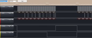
Compiling the above code and deploying it to the STM32 Discovery board generated the following output on the logic analyser:

Polled SPI

Polled SPI

A low clock speed is chosen for the SPI bus as it helps to eliminate the impact of interference from stay signals, long leads etc. Once the system is working at a low clock speed, the prescalar can be changed and the speed increased gradually until we determine the maximum rate at which data can be transmitted reliably.

The main program loop above contains two calls to the SPISend method. The first transmits the data we want top send to the slave device, the second call sends dummy data. This would allow the slave module to send a single byte response.

Interrupt Driven SPI

The final aim of this project is to be able to send data to an LED Panel using SPI. The panel itself is not required to send data back to the application. The modifications made here will take that into consideration. The following changes will be made:

  • Transmit only, no data will be received
  • Interrupt driven
  • Heartbeat will kick off the transmission of the data
  • Transmit a buffer of data (more than a single byte)

The first modification to be made is to the SPI configuration. Change the SPI_InitStruct setup to use a single Tx line and add code to configure the SPI interrupt priority:

SPI_InitStruct.SPI_Direction = SPI_Direction_1Line_Tx;
SPI_InitStruct.SPI_Mode = SPI_Mode_Master;
SPI_InitStruct.SPI_DataSize = SPI_DataSize_8b;
SPI_InitStruct.SPI_CPOL = SPI_CPOL_Low;
SPI_InitStruct.SPI_CPHA = SPI_CPHA_1Edge;
SPI_InitStruct.SPI_NSS = SPI_NSS_Soft | SPI_NSSInternalSoft_Set;
SPI_InitStruct.SPI_BaudRatePrescaler = SPI_BaudRatePrescaler_256;
SPI_InitStruct.SPI_FirstBit = SPI_FirstBit_MSB;
SPI_Init(SPI1, &SPI_InitStruct);
//
//    Configure the SPI interrupt priority
//
NVIC_PriorityGroupConfig(NVIC_PriorityGroup_2);
NVIC_InitStructure.NVIC_IRQChannel = SPI1_IRQn;
NVIC_InitStructure.NVIC_IRQChannelPreemptionPriority = 0;
NVIC_InitStructure.NVIC_IRQChannelSubPriority = 1;
NVIC_InitStructure.NVIC_IRQChannelCmd = ENABLE;
NVIC_Init(&NVIC_InitStructure);

This application will be sending a buffer of data rather than a repeated byte so we need to add somewhere to store the data. Adding the following to the SPI.c file gives us some storage:

//
//    Storage for the SPI data.
//
uint8_t buffer[SPI_BUFFER_LENGTH];
int bufferIndex = 0;

And adding the following to the SPI.h header file allows the storage to be accessible from other modules:

//
//    SPI related constants.
//
#define SPI_BUFFER_LENGTH        10

//
//    Data storage for the SPI methods.
//
uint8_t buffer[SPI_BUFFER_LENGTH];
int bufferIndex;

Ensure that the code is within the extern “C” statement.

The final bit of the puzzle is the addition of the interrupt capability. The method chosen is to configure the SPI bus and leave SPI turned on but initially have the SPI interrupts turned off. The SysTick_Handler will act as the trigger for the SPI communication starting the communication by setting up the initial conditions and turning on the SPI interrupt. The SPI interrupt handler will take over from there. Modifying the SysTick_Handler we get:

//
//    System tick handler.
//
void SysTick_Handler(void)
{
    //
    //    Generate a heartbeat.
    //
    GPIOE->ODR ^= GPIO_Pin_5;
    //
    //    If we are about to generate a rising edge on the heartbeat
    //    we are ready to start SPI data transmission.
    //
    if (GPIOE->ODR & GPIO_Pin_5)
    {
        GPIOE->BSRRH |= GPIO_Pin_6;
        bufferIndex = 0;
        SPI_I2S_ITConfig(SPI1, SPI_I2S_IT_TXE, ENABLE);
    }
}

This code starts the SPI transmission on the rising edge of the heartbeat pulse. Note also that this interrupt handler is responsible for setting the chip select line.

The final bit of the puzzle is the SPI interrupt handler itself.

//
//    Process the interrupts for SPI1.
//
void SPI1_IRQHandler()
{
    //
    //    If TX buffer is empty then transmit the next byte.
    //
    if (SPI1->SR & SPI_I2S_FLAG_TXE)
    {
        if (bufferIndex < SPI_BUFFER_LENGTH)
        {
            SPI1->DR = buffer[bufferIndex++];
        }
    }
    //
    //    If SPI is not busy then we have finished sending data
    //    so turn off this interrupt.
    //
    if (!(SPI1->SR & SPI_I2S_FLAG_BSY))
    {
        SPI_I2S_ITConfig(SPI1, SPI_I2S_IT_TXE, DISABLE);
        GPIOE->BSRRL |= GPIO_Pin_6;
    }
    //
    //    Clear the interrupt pending bit otherwise this interrupt
    //    will be regenerated.
    //
    SPI_I2S_ClearITPendingBit(SPI1, SPI_I2S_IT_TXE);
}

Two key points to notice in this interrupt handler when the end of data buffer has been reached and SPI is no longer busy:

  1. Chip select is set to high
  2. Interrupts are disabled

The last line of this interrupt handler clears the SPI interrupt pending bit to prevent this handler being called again as soon as it exits.

One final modification to be made is to the main program loop. This is no longer required to control the transmission of the data but we will need to setup the contents of the data buffer:

//
//    Main program loop.
//
int main()
{
    Initialise();
    //
    //    Fill the SPI buffer with data.
    //
    int index;
    for (index = 0; index < SPI_BUFFER_LENGTH; index++)
    {
        buffer[index] = index;
    }
    //
    //    Main program loop.
    //
    while (1);
}

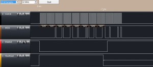
Putting all this together, compiling, deploying gives the following output on the logic analyser:

Buffered SPI With Heartbeat

Buffered SPI With Heartbeat

SPI and DMA

The transition from polled SPI to interrupt driven SPI has so far reduced the load on the microcontroller but the STM32 has one final trick we can use, DMA (Direct Memory Access). DMA allows the various peripherals (of which SPI is one) to directly access the memory used for data storage/retrieval. By doing this the peripheral can operate autonomously until it has run out of data to process.

Remember the following in the SPI interrupt handler above:

if (bufferIndex < SPI_BUFFER_LENGTH)
{
    SPI1->DR = buffer[bufferIndex++];
}

This is required as the SPI peripheral generates an interrupt each time it has transmitted a byte of data and the buffer is empty. With DMA we can hand the SPI peripheral a block of data and tell it to transmit all of the data and simply tell us when the transmission has completed. This means we only receive one interrupt at the end of transmission rather than the 10 we receive for the above scenario.

First thing to do is to modify the InitialiseSPI method to configure the SPI peripheral to use DMA:

//
//    Initialise SPI
//
void InitialiseSPI()
{
    SPI_InitTypeDef SPI_InitStruct;
    NVIC_InitTypeDef NVIC_InitStructure;
    DMA_InitTypeDef DMA_InitStructure;
    //
    //     Connect SPI1 pins to SPI alternate function.
    //
    GPIO_PinAFConfig(GPIOA, GPIO_PinSource5, GPIO_AF_SPI1);
    GPIO_PinAFConfig(GPIOA, GPIO_PinSource6, GPIO_AF_SPI1);
    GPIO_PinAFConfig(GPIOA, GPIO_PinSource7, GPIO_AF_SPI1);
    //
    //    Set PE6 high as we will be using active low for the
    //    device select.
    //
    GPIOE->BSRRL |= GPIO_Pin_6;
    //
    //     Enable the SPI peripheral clock.
    //
    RCC_APB2PeriphClockCmd(RCC_APB2Periph_SPI1, ENABLE);
    //
    //    Configure SPI1 in Mode 0:
    //        CPOL = 0 --> clock is low when idle
    //        CPHA = 0 --> data is sampled at the first edge
    //
    //    SPI Master mode, 8 bits of data, clock prescalar is 128, MSB is
    //    transmitted first.
    //
    SPI_InitStruct.SPI_Direction = SPI_Direction_1Line_Tx;// SPI_Direction_2Lines_FullDuplex;
    SPI_InitStruct.SPI_Mode = SPI_Mode_Master;
    SPI_InitStruct.SPI_DataSize = SPI_DataSize_8b;
    SPI_InitStruct.SPI_CPOL = SPI_CPOL_Low;
    SPI_InitStruct.SPI_CPHA = SPI_CPHA_1Edge;
    SPI_InitStruct.SPI_NSS = SPI_NSS_Soft | SPI_NSSInternalSoft_Set;
    SPI_InitStruct.SPI_BaudRatePrescaler = SPI_BaudRatePrescaler_256;
    SPI_InitStruct.SPI_FirstBit = SPI_FirstBit_MSB;
    SPI_Init(SPI1, &SPI_InitStruct);
    //
    //    Configure the DMA controller
    //
    RCC_AHB1PeriphClockCmd(RCC_AHB1Periph_DMA2, ENABLE);
    DMA_StructInit(&DMA_InitStructure);
    DMA_InitStructure.DMA_Channel = DMA_Channel_3;
    DMA_InitStructure.DMA_PeripheralBaseAddr  = (uint32_t) &(SPI1->DR);
    DMA_InitStructure.DMA_Memory0BaseAddr  = (uint32_t) &buffer;
    DMA_InitStructure.DMA_DIR = DMA_DIR_MemoryToPeripheral;
    DMA_InitStructure.DMA_BufferSize  = SPI_BUFFER_LENGTH;
    DMA_InitStructure.DMA_PeripheralInc  = DMA_PeripheralInc_Disable;
    DMA_InitStructure.DMA_MemoryInc  = DMA_MemoryInc_Enable;
    DMA_InitStructure.DMA_PeripheralDataSize  = DMA_PeripheralDataSize_Byte;
    DMA_InitStructure.DMA_MemoryDataSize  = DMA_MemoryDataSize_Byte;
    DMA_InitStructure.DMA_Mode  = DMA_Mode_Normal;
    DMA_InitStructure.DMA_Priority  = DMA_Priority_High;
    DMA_InitStructure.DMA_FIFOMode  = DMA_FIFOMode_Disable;
    DMA_Init(DMA2_Stream5, &DMA_InitStructure);
    DMA_ITConfig(DMA2_Stream5, DMA_IT_TC, ENABLE);

    NVIC_InitStructure.NVIC_IRQChannel = DMA2_Stream5_IRQn;
    NVIC_InitStructure.NVIC_IRQChannelPreemptionPriority = 0;
    NVIC_InitStructure.NVIC_IRQChannelSubPriority = 1;
    NVIC_InitStructure.NVIC_IRQChannelCmd = ENABLE;
    NVIC_Init(&NVIC_InitStructure);
    //
    //    Enable SPI.
    //
    SPI_Cmd(SPI1, ENABLE);
}

The DMA controller is configured for memory to peripheral data transfer (from the buffer to the SPI->DR register). The pointer into memory is incremented after each transmission but the destination pointer (SPI->DR) remains fixed. The system will use DMA2, channel 3, stream 5. The choice of the DMA peripheral, stream and channel has some freedom but is constrained by the choice of peripheral. The list of allowed choices can be found in the STM32 Programmers Reference. As we are using SPI1 we are forced to use DMA2, channel 3 but we can choose between streams 3 and 5.

The next thing to do is to add a new interrupt handler for the DMA completion interrupt:

//
//    SPI DMA handler.
//
void DMA2_Stream5_IRQHandler()
{
    //
    //     Test if DMA Stream Transfer Complete interrupt
    //
    if (DMA_GetITStatus(DMA2_Stream5, DMA_IT_TCIF5) == SET)
    {
        DMA_ClearITPendingBit(DMA2_Stream5, DMA_IT_TCIF5);
        //
        //    The following is required to ensure that the chip select is not
        //    changed while data is still being transmitted.
        //
        while (SPI_I2S_GetFlagStatus(SPI1, SPI_I2S_FLAG_BSY) == SET);
        //
        //    Now set chip select to high.
        //
        GPIOE->BSRRL |= GPIO_Pin_6;
    }
}

Make a note of the while loop in the middle of the if statement. We will come back to this later.

The final piece of work is to modify the SysTick_Handler method:

//
//    System tick handler.
//
void SysTick_Handler(void)
{
    //
    //    Generate a heartbeat.
    //
    GPIOE->ODR ^= GPIO_Pin_5;
    //
    //    If we are about to generate a rising edge on the heartbeat
    //    we are ready to start SPI data transmission.
    //
    if (GPIOE->ODR & GPIO_Pin_5)
    {
        GPIOE->BSRRH |= GPIO_Pin_6;
        DMA2_Stream5->M0AR = (uint32_t) &buffer;
        DMA_Cmd(DMA2_Stream5, ENABLE);
        SPI_I2S_DMACmd(SPI1, SPI_I2S_DMAReq_Tx, ENABLE);
    }
}

As with the previous interrupt example, this method starts the transfer process.

Putting this together in a project, compiling and deploying gives the following output on the logic analyser:

Multiple DMA SPI Transfers

Multiple DMA SPI Transfers

Remember the while loop above. This is necessary as the DMA transfer complete interrupt is generated as soon as the data has been transferred from memory to the SPI peripheral. This does not necessarily mean that the data has been transferred to the slave device connected to the SPI bus. If we did not have the loop in the handler to check that the transfer had completed we could end up in a situation where the chip select line to taken high before data transfer has completed. This is verified by the following trace on the logic analyser:

Enable Asserting Before Transfer Complete

Enable Asserting Before Transfer Complete

Note how chip select goes high when we still have nearly a full byte of data to transmit.

Conclusion

What started out as an investigation into the control of an LED panel turned into a marathon investigation into SPI on the STM32. This post has presented three different methods for controlling data transfer over SPI each having its own merits. The source code for the CooCox projects can be downloaded here:
  1. Polled SPI
  2. Interrupt driven SPI
  3. SPI and DMA

STM32F4 Clocks

Thursday, March 28th, 2013

The STM32 contains several clocks each of which can be turned on or off when not used. In this post we will examine the clocks available and how they can be configured. To do this we will modify the simple GPIO example to change the clock parameters. Any changes to the system clock speed will increase or decrease the period of the delay. The results can be seen using an oscilloscope. We will look at the following topics:

At the end of this post you should be able to configure the system clock and introduce a known delay subject to the tolerances of the system clocks.

Clock Sources

The STM32 Reference Manual (RM0090) states that there are five clocks available:

  • High Speed Internal (HSI) oscillator
  • High Speed External (HSE) oscillator
  • Phase Locked Loop (PLL)
  • Low Speed Internal (LSI) clock
  • Low Speed External (LSE) clock

As already noted, each clock can be turned on/off as required. Turning an unused clock off reduces the power consumption of the microcontroller.

The first three clocks are used to drive the system clock for the microcontroller. The final two are low speed clocks and are primarily used to drive the watchdogs.

HSI

After reset, the STM32 enables the HSI oscillator. This has a relatively low accuracy, only 1%, but is suitable for most applications. Using the HSI oscillator eliminates the need for an external clock in the final circuit design. On the STM32F4, the HSI oscillator has a clock speed of 16 MHz.

HSE

The STM32 can operate using an external clock circuit. It is possible to design an external clock to run with a greater accuracy than the internal HSI clock enabling finer control of the operating parameters of the final circuit. The exact specification of the external clock frequency varies but is typically 4-16 MHz.

The STM32F4 Discovery Board has a built in external oscillator circuit fitted with a 8 MHz crystal.

PLL

The PLL is used to multiply it’s input clock source by a factor varying between 2 to 16. The input of the PLL is one of HSI, HSE or HSE/2.

It is important to note that the configuration of the PLL cannot be changed once it has been enabled.

LSI

The LSI is a low power clock used for the watchdog timers.

LSE

The LSE is powered by an external 32.768 KHz clock. This provides a method of providing a low speed accurate clock for the real time clock.

System and Peripheral Clocks

Once the clock source has been selected it is necessary to configure the internal system and peripheral clocks. The internal clocks are:

  • System Clock
  • Advanced High Performance Bus (AHB)
  • Low speed Advanced Peripheral Bus (APB1)
  • High speed Advanced Peripheral Bus (APB2)

Each of these clocks can be scaled using prescalers. A fuller picture of the types of clocks and their relationships can be found in the STM32 Reference Manual (RM0090).

System Clock

The system clock is used to determine the speed at which instructions are executed and has a maximum speed of 168MHz.

Advanced High Performance Bus (AHB)

Derived from the system clock, this bus has a maximum speed of 168MHz.

Low speed Advanced Peripheral Bus (APB1)

Derived from AHB, this bus has a maximum speed of 42MHz.

High speed Advanced Peripheral Bus (APB2)

Derived from AHB, this clock has a maximum frequency of 84MHz.

Non-System Clock Peripherals

A number of the peripheral clocks are not derived from the system clock but have their own independent source.

USB OTG FS, Random Number Generator and SDIO Clock

These clocks are all driven by an independent output of the PLL. The maximum speed for these peripherals is 48MHz.

I2S

The I2S peripherals have their own internal clock (PLLI2S). Alternatively, this can be derived by an independent external clock source.

USB OTG HS and Ethernet Clock

These clocks are derived from an external source.

Microcontroller Clock Output

The STM32 provides the ability to output up to two clocks to the external circuit using the Microcontroller Clock Output (MCO) pins. Both of the outputs can have a prescaler applied. This can be in the range 1 to 5 inclusive.

Microcontroller Clock Output 1 (MCO1) is output on pin PA8. MCO1 output can be one of HSI, LSE, HSE or PLL scaled appropriately.

Microcontroller Clock Output 2 (MCO2) is output on pin PC9. MCO2 output can be one of HSE, PLL, System Clock or PLLI2S scaled appropriately.

The clock output is configured by selecting the appropriate alternative function for the GPIO port and is restricted to 100MHz.

Configuring the Clock

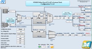
The number of features on the STM32F4 analysis and discussion of the registers and their function large. Luckily ST have come to the rescue and provided a configuration tool to help.

ST Clock Configuration Tool in Wizard Mode

ST Clock Configuration Tool in Wizard Mode

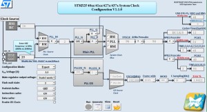
This Excel spreadsheet can be run in both Expert and Wizard mode making it suitable for a wide range of users.

ST Clock Configuration Tool in Expert Mode

ST Clock Configuration Tool in Expert Mode

The grey number in the above illustration have been calculated whilst the numbers in black can be changed by the users.

The output from this spreadsheet is a source file (system_stm32f4xx.c) which can be added to your project. This file, system_stm32f4xx.c, contains three methods which can be called to setup the clocks on the microcontroller:

  • SystemInit – Setup the system including the clocks
  • SystemCoreClockUpdate – Setup the SystemCoreClock variable (clock frequency)
  • SetSysClock – Setup the system clock (called from SystemInit)

We can see the effect of calling SystemInit by using the code from the simple GPIO example to the following:

#include "stm32f4xx_rcc.h"
#include "stm32f4xx_gpio.h"
#include "system_stm32f4xx.h"

int main()
{
    //
    //  Uncomment this line to see the effect of
    //  the clock change.
    //
	//SystemInit();
    //
    //  Initialise the peripheral clock.
    //
    RCC->AHB1ENR |= RCC_AHB1Periph_GPIOD;
    //
    //  Initialise the GPIO port.
    //
    GPIOD->MODER |= GPIO_Mode_OUT;
    GPIOD->OSPEEDR |= GPIO_Speed_100MHz;
    GPIOD->OTYPER |= GPIO_OType_PP;
    GPIOD->PUPDR |= GPIO_PuPd_NOPULL;
    //
    //  Toggle Port D, pin 0 indefinitely.
    //
    while (1)
    {
        GPIOD->BSRRL = GPIO_Pin_0;
        GPIOD->BSRRH = GPIO_Pin_0;
    }
}

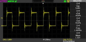
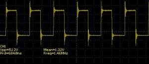
If we run the code above with the SystemInit line commented out and hook an oscilloscope up to pin 0 of port D we get a square wave output with a frequency of about 1.5MHz.

STM32F4 Output (1.46MHz)

STM32F4 Output (1.46MHz)

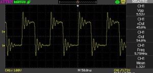
Now uncomment the SystemInit line of code and re-run the example. This time we see that the output signal has a frequency of nearly 4.9MHz.

STM32F4 Output (5.75MHz)

STM32F4 Output (5.75MHz)

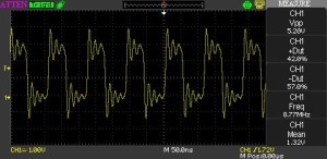
Turning the configuration tool into expert mode and tweaking a few of the parameters allows the frequency of the output signal to go to 8.77MHz.

STM32F4 Output (8.77MHz)

STM32F4 Output (8.77MHz)

Timings are based upon the optimisation level being set to no optimisation. Turning the optimisation on to the maximum speed allows an output signal of nearly 20MHz to be generated.

Conclusion

The STM32 contains a variety of clock sources and configuration using the registers within the microcontroller would be a complex task. The Clock Configuration tool eases the configuration of the internal and peripheral clocks generating the source code for system_stm32f4xx.c automatically.

The Clock Configuration tool and the associated guide can be downloaded from ST’s web site. The tool and document are in the following files:

  • stsm-stm32091 Clock Configuration Tool
  • AN3988 Clock Configuration Tool User Guide

CooCox – ARM Development Environment For the Beginner

Saturday, March 23rd, 2013

A few weeks ago I published two articles on development environments for the STM32F4 Doscovery Board. Since then I have become aware of CooCox IDE. This is a small development environment for a number of Microcontrollers including some of the STM32 range of processors.

The IDE promises to be free, unrestricted and simple offering the ability to develop high-quality software solutions in a timely and cost effective manner.

Too good to be true?

Let’s find out.

Web Site

I must admit, it took me a long time to take this tool seriously. I found the web site in the very early days in my search for a reasonable cost development environment for the STM32F4 Discovery board. The look and feel of the site left me a little cold. The design looks like it was put together in the early 1990s.

My only hope was that the tools were better.

Clicking through to the CoIDE page promised to show a video instead I found myself presented with a large amount of white space where the video should be. Maybe this works with IE or Firefox but not with Chrome. If you do see the white spave please take the time to scroll to the bottom of the page. There you will find tables detailing the supported chips/boards along with some download links.

On the whole this web site left me feeling nervous and I must admit that the first time I came across this tool I dismissed it purely based upon the look and feel of the web site.

So what made me come back, a comment made by a colleague, i.e. it worked and was simple to use.

Software

In order to use this IDE to develop applications for your board you also need to download the ARM GCC 4.7 toolchain. This is the same toolchain I used when setting us Eclipse to work with the STM32F4 Discovery board (see Setting up GCC for the STM32F4 Discovery Board). I was lucky enough to have this toolchain already installed making one less task to perform.

Downloading the IDE is simple although you do need to register on the site.

Installation was painless and the initial setup was also simple.

I’m starting to get over the feeling of unease I experienced when I first visited the web site.

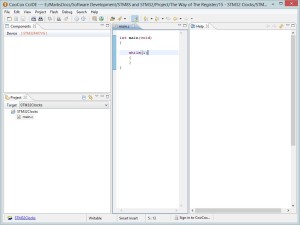
Starting the IDE present you with a very familiar look and feel:

New Project

New Project

It feels like Eclipse.

Creating a Project

Let’s see how good the environment is by taking the code from STM32 – Simple GPIO and Some Flashing LEDs post.

Creating a new project is simple, just head over to the Project->New Project menu item. Doing this will present you with a wizard which will take you through the steps required to select your board and create an empty project.

Some hints:

  • When creating a new project you need to untick the Use default path option if you want your code to be put anywhere other than under the installation directory.
  • The select board or chip does not have an option for the STM32F4 Discovery Board (or any for the Discovery boards for that matter). To use this board select Chip and then locate the STM32F407VG chip.

Upon completion of the wizard you will be presented with the component selection tab in the IDE:

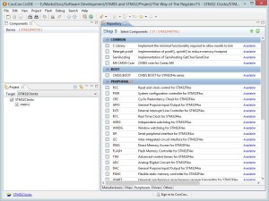
Component Selection

Component Selection

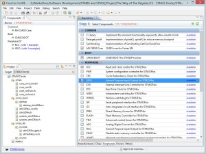
This tab is really powerful and makes it easy for the new comer to this board to get off the ground. In the previous example I used two sets of definitions; Reset and clock control and GPIO. Ticking the RCC option in the component tab automatically adds the headers and source files needed to use the RCC library to the project. It also adds any dependencies, in this case the CMSIS core system startup files. After selecting the RCC and GPIO components the IDE looks as follows:

Initial Component Selection

Initial Component Selection

Opening file explorer on the PC showed that the directory structure had been modified and the files put in place. So what happens if you untick and option? Removing components removes the files from the project and it also removes them from file store as well.

Now this feature may seem simple but for the beginner it is really powerful. It ensures that all of the source and header files required are added to the project. This is something which whilst not difficult can trip up the beginner. It is also a little tedious to do with IAR and Eclipse.

One downside of the component selection tab is that it does not easily allow you to remove the source code for the components you have added without also removing the header files as well. I am following the principle of The Way of the Register and not using the Standard Peripheral Library. This requires the header files but not the source code for the library itself. We can only hope the linker is smart enough to remove unused code from the final object executable.

Building the project is as simple as clicking on the Build icon (or using the Project->Build menu item). A few seconds later I have the default applicaiton and the library files compiled.

Debugging

An IDE is really nothing without a reasonable debugger. I remember from the work I did setting up Eclipse (see Setting up GCC for the STM32F4 Discovery Board) that Eclipse needed the OpenOCD library in order to be able to debug an application using ST-Link. There is no mention of OpenOCD when using CooCox. The only additional software required for debugging appears to be the ST-Link USB driver. Again, I already have this installed but you may need to visit ST’s web site for the latest version.

In order to debug we need some code so let’s borrow the code from the Simple GPIO example:

#include "stm32f4xx_rcc.h"
#include "stm32f4xx_gpio.h"

int main()
{
    //
    //  Initialise the peripheral clock.
    //
    RCC->AHB1ENR |= RCC_AHB1Periph_GPIOD;
    //
    //  Initialise the GPIO port.
    //
    GPIOD->MODER |= GPIO_Mode_OUT;
    GPIOD->OSPEEDR |= GPIO_Speed_25MHz;
    GPIOD->OTYPER |= GPIO_OType_PP;
    GPIOD->PUPDR |= GPIO_PuPd_NOPULL;
    //
    //  Toggle Port D, pin 0 indefinitely.
    //
    while (1)
    {
        GPIOD->BSRRL = GPIO_Pin_0;
        GPIOD->BSRRH = GPIO_Pin_0;
    }
}

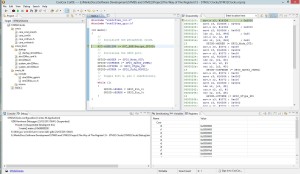
Starting the debugger (Ctrl-F5) changes the IDE context and presents the debugging interface with the application stopped at the first line of code:

CooCox debugging aspect

CooCox debugging aspect

Warning – the above image is large

Pressing F5 runs the application to the next breakpoint. As I have not set any breakpoints this should run the application indefinitely and indeed it does. Hooking up the scope to pin 0 of port D shows the following output:

Scope output

Scope output

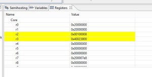
Single stepping is achieved using F10 and F11. So re-running the application and pressing F10 should single step over the current line of code and indeed it does. The registers window also highlights the ARM registers that were changed by executing the last instruction:

Register View

Register View

One thing that I have found missing which I really appreciate with IAR is the ability to view the state of the peripheral registers (as opposed to the microcontroller registers). This is a really useful feature as it means you do not have to locate the registers in memory and decode them yourself.

Conclusion

CooCox IDE is a simple way to get into working with the STM32F4 Discovery board. The power and simplicity of the tool is only let down by the dated look of the web site.

A cracking tool; well worth looking at.

STM32 – Simple GPIO and Some Flashing LEDs

Saturday, March 23rd, 2013

When starting with a new development board I always revisit the fundamentals like GPIO. Doing this helps establish that the development tools are working and gives a basic library for future development. So with this post we will be looking at GPIO on the STM32 Discovery board. When Rediscovering the STM32 Discovery Board I mentioned that I would need to look at using either the standard peripheral library provided by ST or to use a lower level method of controlling the board. After due consideration I have decided to continue with the lower level access. Whilst this may be more effort it does lead to a better understanding of what is actually happening at the low level.

Our objective today will be to toggle a GPIO pin (Port D, pin 0) generating a square wave. The result will be something similar to the Simple GPIO post for the STM8S.

STM32F4 Discovery Board

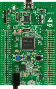
The STM32F4 Discovery board is a low cost development board for hobbyists, beginners and experienced users. The board uses the STM32F407VGT6 and hosts a number of sensors including digital accelerometer, push buttons, microphone and DAC. It also contains four built in LEDs which can be used to give feedback to the developer and breakout pins for the GPIO ports.

STM32F4 Discovery Board

STM32F4 Discovery Board

Each of the GPIO pins can be used for simple input/output of digital signals. The majority of the pins are also mapped to one or more alternative functions. For instance, Port C, pin 3 is also mapped to the following alternative functions:

  • SPI2 MOSI
  • I2S2 SD
  • OTG HS ULPI NXT
  • ETH MI TX Clk
  • EVENTOUT

For the remainder of this post we will restrict ourselves to the GPIO functionality of the chip and demonstrate the following:

  • Output a digital signal on a single GPIO pin
  • Flash one of the LEDs on the board

The alternative functionality will be considered in future posts.

The functionality of the 16 pins on each of the GPIO ports is controlled by a number of registers. The description of each of the registers can be found in RM0090 Reference Manual for the STM32 chip. This manual can be downloaded from STs web site.

GPIO Registers

Each STM32 chip has a number of ports each of which has 16 pins. As already noted, each of these pins has a number of functions, the most basic of which is digital input/output. The functionality and state of each port is controlled by a number of GPIO registers:

  • Four configuration registers
  • Two data registers
  • One set/reset register
  • One locking register
  • Two alternative function registers

An overview of the registers follows; a fuller description of the registers can be found in section 7 of RM0090 Reference Manual (Revision 4).

When referring to the registers, the reference manual uses the following notation:

GPIOx_Function

Where x is replaced by the port to be used. For instance, GPIOx_MODER refers to the generic mode register for a GPIO port. A specific instance of this would be GPIOD_MODER. This refers to the mode register for port D. Normally, x is in the range A to I and is defined by the specific version of the STM32 being used in the project.

Configuration Registers

The STM32 has four configuration registers for each of the ports.

  • Port mode register – GPIOx_MODER
  • Output type register – GPIOx_OTYPER
  • Speed register – GPIOx_OSPEEDR
  • Pull-up/Pull-down register – GPIOx_PUPDR

Each of these registers is 32-bits wide although not all of the bits are used in all of the registers.

Port Mode Register – GPIOx_MODER

This 32 bit register holds 2 bit values which defines the operation mode. The modes allowed are:

Bit ValuesDescription
00Input
01General purpose output
10Alternate function
11Analog

In general, the default reset value for this register is 0. Some of the ports are reset to non-zero values as the pins in the port have special meanings (debugging pins etc). The rest values are:

PortReset Value
A0xA800 0000
B0x0000 0280
All others0x0000 0000

The bits in the register are read/write and are in consecutive pairs. So bits 0 & 1 define the mode for pin 0, bits 2 & 3 define the mode for pin 1 etc.

Output Type Register – GPIOx_OTYPER

This is a 32-bit register but only the lower 16 bits are used. The top 16 bits are reserved and should not be used. This register uses a single bit for each pin to define the output type of the pins in the port. So, bit 0 defines the output type for pin 0, bit 1 for pin 1 etc.

Bit ValueDescription
0Push/pull output
1Open drain output

The default reset value for all of the GPIOx_TYPER registers is 0x0000 0000 meaning that all ports are configured for push/pull output.

Speed Register – GPIOx_OSPEEDR

This 32-bit register uses all of the bits in the register in pairs (similar to the port mode register). The bits define the output speed of the port. The bit pairs have the following meaning:

Bit ValuesDescription
002 MHz Low speed
0125 MHz Medium speed
1050 MHz Fast speed
11100 MHz High speed on 30pF
80 MHz High speed on 15 pF

The reset value for these registers is 0x0000 00C0 for port B and 0x0000 0000 for all other registers.

Pull-up/Pull-down register – GPIOx_PUPDR

This 32-bit register uses all of the bits in the register in pairs (similar to the port mode register). The bits define pull-up / pull-down resistor mode for the pins on a port. The bit pairs have the following meaning:

Bit ValuesDescription
00No pull-up or pull-down resistor
01Pull-up resistor
10Pull-down resistor
11Reserved

The reset values for the registers are:

PortReset Value
A0x6400 0000
B0x0000 0100
All others0x0000 0000

Data Registers

The two data registers for each port indicate the input/output state of the port. Each of the registers are 32-bit registers but only the lower 16 bits are used. The top 16 bits are reserved and should not be used.

  • Input data register – GPIOx_IDR
  • Output data register – GPIOx_ODR

Input data register – GPIOx_IDR

The input data register indicates if a high or low signal has been applied to the pin within a port. The register is read-only and the whole word should be read.

Bit ValueDescription
0High logic value
1Low logic value

As with the output type register – GPIOx_OTYPER, the bits in the register map onto the pins in the port (bit 0 maps to pin 0, bit 1 to pin 1 etc.).

The reset value for all of these registers is 0x0000 XXXX where X indicates that the bits are unknown as they will be defined by the input signals applied to the pins are reset.

Output data register – GPIOx_ODR

The output data register allows the program to change the output state of a pin within the port. This is a 32-bit register and only the lower 16 bits are used. The top 16 bits are reserved and should not be used. The output states are defined as:

Bit ValueDescription
0High logic value
1Low logic value

As with the output type register – GPIOx_OTYPER, the bits in the register map onto the pins in the port (bit 0 maps to pin 0, bit 1 to pin 1 etc.). The bits in the lower 16 bits of the register are all read/write bits.

The reset value for all of these registers is 0x0000 0000.

A more effective way of setting/resetting a bit in the output register is to use the bit set/reset register.

Set/reset register

The set/reset register sets or resets a single bit in the output data register.

Bit Set/Reset Register – GPIOx_BSSR

This is a 32-bit register and it is split into two halves, the lower 16 bits are used for setting a bit and the upper 16 bits are used for resetting a bit. This is a write only register; reading this register will return 0x0000.

Setting a bit in the lower 16-bits of this register will cause the corresponding bit in the output data register to be set to 1.

Similarly, setting a bit in the upper 16-bits of this register will cause the corresponding bit in the output data register to be set to 0.

For the lower 16-bits the mapping is simple, bit 0 in GPIOx_BSRR maps to bit 0 in GPIOx_ODR etc. For the upper 16-bits, bit 16 of the GPIOx_BSRR maps to bit 0 of the GPIOx_ODR; bit 17 of GPIOx_BSRR maps to bit 1 of GPIOx_ODR etc.

So why provide the set/reset functionality when you have the output data registers? The set/reset register provide an atomic method of setting or resetting an output pin on a port. When using the output data registers, the compiler will have to generate a number of statements in order to set or reset a pin. This can allow an interrupt to be processed when part way through the set/reset operation. By using this register it is possible to set or reset a pin using a single instruction. This means that the operation will complete before the interrupt can be processed.

Configuration Lock Register

This register is used to lock the configuration of the port until the next reset of the chip.

Configuration Lock Register – GPIOx_LCKR

The register is a 32-bit register but only 17 bits are actually used. The lower 16 bits indicate which bit of the port configuration is locked. So setting bit 0 of the register will lock the configuration of pin 0 etc.

The final bit used is bit 16 in the register (known as the Lock Key – LCKK); this bit determines the lock status of the port; a zero indicates that no lock is applied whilst a 1 indicates that the port configuration is locked.

In order to lock the configuration of a port the configuration lock write sequence must be followed. This will prevent accidental locking of the port configuration. The algorithm for locking the configuration is as follows:

  • Set bits 0 through 15 of the register indicating which pins should have their configuration locked
  • Set LCKK to 1 and write the value into the register
  • Set LCKK to 0 and write the value into the register
  • Set LCKK to 1 and write the value into the register
  • Read the lock bit of the port

It is important to note that the values in bits 0 through 15 should not change whilst following the above sequence. Should they change or any error occur then the lock will be aborted.

The final step, reading the lock bit, confirms the success or failure of the operation.

Alternative function registers

The alternative function registers allow the configuration of the port to change from simple GPIO to an alternative function such as SPI MOSI. These registers are noted here but will not be discussed further as they will be covered in subsequent posts.

C Definitions and Some Typedefs

The register in the STM32 microcontroller have been mapped onto specific memory locations within the valid address space of the STM32. These memory locations are defined in the various header files for the microcontroller. For instance, the following type definition has been taken from the header file stm32f4xx.h:

typedef struct
{
  __IO uint32_t MODER;    /*!> GPIO port mode register,               Address offset: 0x00      */
  __IO uint32_t OTYPER;   /*!> GPIO port output type register,        Address offset: 0x04      */
  __IO uint32_t OSPEEDR;  /*!> GPIO port output speed register,       Address offset: 0x08      */
  __IO uint32_t PUPDR;    /*!> GPIO port pull-up/pull-down register,  Address offset: 0x0C      */
  __IO uint32_t IDR;      /*!> GPIO port input data register,         Address offset: 0x10      */
  __IO uint32_t ODR;      /*!> GPIO port output data register,        Address offset: 0x14      */
  __IO uint16_t BSRRL;    /*!> GPIO port bit set/reset low register,  Address offset: 0x18      */
  __IO uint16_t BSRRH;    /*!> GPIO port bit set/reset high register, Address offset: 0x1A      */
  __IO uint32_t LCKR;     /*!> GPIO port configuration lock register, Address offset: 0x1C      */
  __IO uint32_t AFR[2];   /*!> GPIO alternate function registers,     Address offset: 0x20-0x24 */
} GPIO_TypeDef;

This header file can be found in the Standard Peripheral Library as supplied by ST Microelectronics.

A careful examination of the members of the struct within the typedef reveals that with one exception, the members of the struct all map directly onto the registers we have been discussing above. The one exception is the BSSR register. This has been split into two components BSSRL and BSSRH. This split nicely maps to the difference in functionality of the two halves of the register, namely Setting and resetting of individual bits in the output data register.

Locating A GPIO in Memory

Once we have the layout of the registers (as defined in the struct above), we simply need to map the structure onto the right location in memory. A little further digging in the header file leads us to the following #define statements:

#define GPIOD             ((GPIO_TypeDef *) GPIOD_BASE)

#define GPIOD_BASE        AHB1PERIPH_BASE + 0x0C00)

#define APB1PERIPH_BASE   PERIPH_BASE

#define PERIPH_BASE       ((uint32_t) 0x40000000) /*!< Peripheral base address in the alias region                                */

Following the chain of #define statements leads us to the the conclusion that the registers for GPIOD are located at memory location 0x40000C000. These definitions mean that we should be able to access individual registers with statements such as:

GPIOD->MODER = 0x01;    // Set Pin 0 of Port D to input.

A Practical Demonstration

After all this theory we must be ready for some coding. In this section we will look at creating two small applications:

  • GPIO Toggle – toggling a single pin on a GPIO port
  • Blinky – Flashing a single LED

The first of the two applications will simply toggle a single GPIO pin as fast as possible using the default reset state of the microcontroller. Note that an oscilloscope will be required in order to prove that the application is working correctly

The second application will make use of the on board LEDs. This will require a little more coding in order to provide a delay between turning the LED on and off in order to make the flashing visible to the naked eye.

Application 1 – Toggling A GPIO Pin

This application is simple and consists of two parts:

  • Initialisation
  • A loop which toggles the GPIO pin

The full application looks like this:

#include "stm32f4xx_rcc.h"
#include "stm32f4xx_gpio.h"

int main()
{
    //
    //  Initialise the peripheral clock.
    //
    RCC->AHB1ENR |= RCC_AHB1Periph_GPIOD;
    //
    //  Initilaise the GPIO port.
    //
    GPIOD->MODER |= GPIO_Mode_OUT;
    GPIOD->OSPEEDR |= GPIO_Speed_25MHz;
    GPIOD->OTYPER |= GPIO_OType_PP;
    GPIOD->PUPDR |= GPIO_PuPd_NOPULL;
    //
    //  Toggle Port D, pin 0 indefinitely.
    //
    while (1)
    {
        GPIOD->BSRRL = GPIO_Pin_0;
        GPIOD->BSRRH = GPIO_Pin_0;
    }
}

One thing to note from the above code is that we need to initialise the peripheral clocks (this should be taken as read for the moment and will be covered in future posts). When initialising the GPIO port we should take into consideration the default clock speed of the Discovery board after reset. By default this is 8 MHz and so we should set the speed of the output port accordingly. This leads to a configuration for pin 0 of output with a maximum speed of 25 MHz, push pull with not pull-up or pull-down resistors.

Once initialised we enter the main program loop. Here the application uses the set/rest registers to toggle pin 0. This shows how the 32-bit register is split into two, one for the set and one for the reset operation.

If we create a simple STM32 project using IAR, compile and then deploy this application we get the following output on the oscilloscope:

STM32 Scope Output

STM32 Scope Output

And there we have it, our first application deployed to the STM32 Discovery board.

Blinky – Flashing A Single LED

This second example is really aimed at those who do not have access to an oscilloscope. Here we will slow down the output of the GPIO port and flash one of the built in LEDs.

The STM32F4 Discovery board has four built in LEDs which can be accessed by setting/resetting pin 12 through 15 on port D. The LED colours are:

Pin NumberColour
12Green
13Orange
14Red
5Blue

Using the code in the previous example as a starting point we find ourselves with an application which looks something like this:

#include "stm32f4xx.h"
#include "stm32f4xx_gpio.h"
#include "stm32f4xx_rcc.h"

#define LED_GREEN      12
#define LED_ORANGE     13
#define LED_RED        14
#define LED_BLUE       15

int main()
{
    int pin = LED_RED;
    uint32_t mode = GPIO_Mode_OUT << (pin * 2);
    uint32_t speed = GPIO_Speed_100MHz << (pin * 2);
    uint32_t type = GPIO_OType_PP << pin;
    uint32_t pullup = GPIO_PuPd_NOPULL << (pin * 2);
    //
    //  Initialise the peripheral clock.
    //
    RCC->AHB1ENR |= RCC_AHB1Periph_GPIOD;
    //
    //  Initilaise the GPIO port.
    //
    GPIOD->MODER |= mode;
    GPIOD->OSPEEDR |= speed;
    GPIOD->OTYPER |= type;
    GPIOD->PUPDR |= pullup;
    //
    //  Toggle the selected LED indefinitely.
    //
    int index;
    while (1)
    {
        GPIOD->BSRRL = (1 << pin);
        for (index = 0; index < 500000; index++);
        GPIOD->BSRRH = (1 << pin);
        for (index = 0; index < 500000; index++);
    }
}

Deploying this application should flash the selected LED just below the STM32 microcontroller on the STM32F4 Discovery board.

Conclusion

This post presented two simple applications which toggle GPIO lines on Port D. Using these techniques and the additional information in the register descriptions you should be able to extend the application above to control digital devices such as shift registers etc.

Setting up GCC for the STM32F4 Discovery Board

Friday, March 8th, 2013

A few days ago I wrote this post about the STM32 Discovery board and my experiences setting this board up with the IAR Embedded Workbench Kickstarter for ARM. In that post I mentioned that there are some free development tools available for this board, namely the GCC tool chain. I was going to leave these tools until I reached the point where I needed to remove the code size restriction which is in place for the IAR toolset.

Well I could not resist investigating this tool chain further.

Installing the Software

A quick visit to Google lead me to Hussam Al-Hertani’s blog where there are a number of articles which discuss setting up the GCC tool chain for the STM32F0 Discovery board. These three articles provide a comprehensive overview of the steps you need to follow:

Also included on the blog is an overview of the GCC compilation process.

The two boards (STM32F0 and STM32F4) should be similar and so I decided to give the above a go and see if I could use the GCC tools with the STM32F4 Discovery board.

Installing the Tools

The installation process went reasonably well with only a couple of issues.

Part 1 – Setting up the GCC ARM Toolchain

The installation of the tools went according to the blog until we reached the instructions to compile the sample application. The main problem here was that the application would not compile due to missing header files. This problem was caused by the differences in the directory names and structure of the firmware libraries. The only changes required were to the include and library variables in the makefile.

Part 2 – Setting up the Eclipse IDE

Setting up Eclipse was completed without any issues.

Part 3 – Setting up Debugging with the Eclipse IDE (OpenOCD 0.6.x)

Setting up OpenOCD and connecting this to Eclipse was also straightforward.

Creating A New Example

Remember this code:

GPIO_InitTypeDef  GPIO_InitStructure;

RCC_AHB1PeriphClockCmd(RCC_AHB1Periph_GPIOD, ENABLE);
int flag = 0;
GPIO_InitStructure.GPIO_Pin = GPIO_Pin_0;
GPIO_InitStructure.GPIO_Mode = GPIO_Mode_OUT;
GPIO_InitStructure.GPIO_OType = GPIO_OType_PP;
GPIO_InitStructure.GPIO_Speed = GPIO_Speed_100MHz;
GPIO_InitStructure.GPIO_PuPd = GPIO_PuPd_NOPULL;
GPIO_Init(GPIOD, &GPIO_InitStructure);
while (1)
{
    if (flag)
    {
        GPIO_SetBits(GPIOD, GPIO_Pin_0);
        flag = 0;
    }
    else
    {
        GPIO_ResetBits(GPIOD, GPIO_Pin_0);
        flag = 1;
    }
}

In order to generate a new example we start with the code we have compiled and working. There are very few changes required. Theses are main made in the make file. We remove the files which are not required and then verify that the libraries and include files can be accessed by the compiler.

The final change is to replace the code in main.c with our code above.

Compilation and deployment from within Eclipse went as expected and the application ran with no issues.

How About Debugging?

With Eclipse open and the above project loaded I set a breakpoint on the first line of the application. Starting the debugger stopped the application at the first line of code – things are looking good. Single stepping also appeared to look as though it was working well at first. A few lines further on and this is where the issues started. The debugger and the line of source code started to get out of step. The IDE would skip a line of code in a consistent manner. It looks like the debugger information is slightly out of sync with the breakpoints. After spending a little time looking at this I found that the original makefile I have been using had the optimisation level set to -Os. The debugger/IDE started to behave as expected when I changed this to -O0.

Conclusion

The installation of the GCC development environment was simple enough and the instructions on Hertaville are comprehensive and well worth visiting. It is always good to have a free unlimited development environment.

Change Log:

  • 10th March 2013: Added additional information about the optimisation flag in the build file.