The Raspberry Pi is classically used as a single board computer running Linux but it also offers the possibility of using the board without Linux (known as bare metal development). Add to this the availability of free ARM development tools and we have the opportunity to develop on a high speed ARM processor at a reasonable cost.
This post explores the steps necessary to toggle a GPIO pin on the Raspberry Pi by directly accessing the registers without the presence of an operating system.
Project Description
For this simple project the software will need to perform three operations:
Configure the GPIO port
Set the GPIO pins for the selected port
Reset the GPIO pins for the selected port
The application here will toggle two GPIO pins, one connected to one of the LEDs on the board (GPIO16 connected to the OK/ACT LED) and the second connected to a pin on the header (GPIO18 connected to Pin 12 on header P1).
Resources
There are already a number of resources out on the internet which cover this topic including a large number references in the Bare Metal forum on the Raspberry Pi web site.
As well as the Raspberry Pi web site there are a number of other sites discussing OS development for the Raspberry Pi. This post was going to be a comprehensive write up of the tools and various scripts required to put together a bare metal example but I have since discovered an excellent tutorial on this subject on the OSDev web site. I would heartily recommend that you visit this web site and review the material on the Raspberry Pi C Tutorial page.
Hardware
Before we look at the registers we need to take a look at the first chapter of the Broadcom BCM2835 ARM Peripheral document. Particularly the following two paragraphs:
Physical addresses range from 0x20000000 to 0x20FFFFFF for peripherals. The bus addresses for peripherals are set up to map onto the peripheral bus address range starting at 0x7E000000. Thus a peripheral advertised here at bus address 0x7Ennnnnn is available at physical address 0x20nnnnnn.
and
The peripheral addresses specified in this document are bus addresses. Software directly accessing peripherals must translate these addresses into physical or virtual addresses, as described above. Software accessing peripherals using the DMA engines must use bus addresses.
The remainder of the document discusses the registers and uses addresses in the 0x7Ennnnnn-0x7EFFFFFF memory range. This means that any software written should translate the 0x7Ennnnnn range down to the 0x20nnnnnn range.
GPIO Configuration Register
The software will need to set the function for GPIO pins 16 and 18 using the function select registers. The description of these registers and the GPIO pins which they relate to can be found on page 92 of the Broadcom BCM2835 ARM Peripheral manual. The port is configured using three bits in the register. The three bits have the following meaning:
Bit Field
Description
000
GPIO Pin is an input
001
GPIO Pin is an output
100
GPIO Pin configured for alternate function 0
101
GPIO Pin configured for alternate function 1
110
GPIO Pin configured for alternate function 2
111
GPIO Pin configured for alternate function 3
011
GPIO Pin configured for alternate function 4
010
GPIO Pin configured for alternate function 5
The two pins the software will be accessing are pins 16 and 18. These pins are configured using bits 24-26 for GPIO 18 and 18-20 for GPIO 16 of the GPFSEL1 register at 0x7E200004. This maps to the address 0x20200004.
Set GPIO Pin High
The GPIO pins are set by setting a bit in the GPSETn registers. Both GPIO16 and GPIO18 are set through the GPSET0 register (see page 95 of the Broadcom BCM2835 ARM Peripheral manual). The address of this register is 0x7E20001C (0x2020001C).
Set GPIO Pin Low (Clear the GPIO Pin)
The GPIO pins are reset by setting a bit in the GPCLRn registers. Both GPIO16 and GPIO18 are set through the GPCLR0 register (see page 95 of the Broadcom BCM2835 ARM Peripheral manual). The address of this register is 0x7E200028 (0x20200028).
Software
The application is a relatively simple one, toggling a GPIO pin continuously. The following should suffice:
//
//  Flags used to configure the GPIO port.
//
#define FLAG_GPIO_RESET     ((7 << 18) | (7 << 24))
#define FLAG_GPIO_CONFIG    ((1 << 18) | (1 << 24))
//
//  Bits which will allow control of GPIO0 pins for the status
//  LED and the header on the Pi.
//
#define GPIO_PINS           ((1 << 16) | (1 << 18))
//
//  The following register definitions are used to access the GPIO
//  pins on the BCM2835.  The register definitions are taken from
//  section 6 of the BCM manual and the mapping is described in
//  section 1 of the same.
//
//  Address of the register which will configure the GPIO pins.
//
volatile unsigned int *gpsel1 = (unsigned int *) 0x20200004;
//
//  Address of the register which will set the GPIO pins.
//
volatile unsigned int *gpset0 = (unsigned int *) 0x2020001C;
//
//  Address of the register which will clear the GPIO pins.
//
volatile unsigned int *gpclr0 = (unsigned int *) 0x20200028;
//
//  Contents of the GPIO configuration register.
//
unsigned int gpioConfig;
//
//  Main program loop.
//
int main()
{
    //
    //  Reconfigure GPIO 16 and 18 to be outputs.  Clear any
    //  previous GPIO configuration for these pins.
    //
    gpioConfig = *gpsel1;
    //
    //  Firstly, remove any configuration for GPIO 16 & 18.
    //
    gpioConfig &= ~FLAG_GPIO_RESET;
    //
    //  Now configure GPIO 16 & 18 to be plain GPIO outputs.
    //
    gpioConfig |= FLAG_GPIO_CONFIG;
    *gpsel1 = gpioConfig;
    //
    //  Toggle GPIO 16 and 18 forever.
    //
    while (1)
    {
        *gpclr0 = GPIO_PINS;
        *gpset0 = GPIO_PINS;
    }
    return(0);
}
The makefile I used to build the application looks as follows:
#
#   Root directory/name of the ARM tools used to build the application.
#
ARMTOOLSROOT = e:\utils\gcc-arm\bin\arm-none-eabi

#
#   C Compiler options.
#
OPTIONS = -nostdlib -ffreestanding -O3

#
#   What do we need to make to build everything?
#
all: kernel.img
    copy /y /d kernel.img j:\

HelloWorldBlinky.o : HelloWorldBlinky.c
	$(ARMTOOLSROOT)-gcc $(OPTIONS) -c HelloWorldBlinky.c -o HelloWorldBlinky.o

HelloWorldBlinky.elf : memmap HelloWorldBlinky.o
	$(ARMTOOLSROOT)-ld HelloWorldBlinky.o -T memmap -o HelloWorldBlinky.elf
	$(ARMTOOLSROOT)-objdump -D HelloWorldBlinky.elf > HelloWorldBlinky.list

kernel.img : HelloWorldBlinky.elf
	$(ARMTOOLSROOT)-objcopy HelloWorldBlinky.elf -O binary kernel.img

#
#   Delete any previously built files.
#
clean :
	del -f HelloWorldBlinky.o
	del -f HelloWorldBlinky.elf
	del -f HelloWorldBlinky.list
	del -f kernel.img
Tools
The software present here was compiled using the version 4.8.3 of the ARM eabi tools.
Conclusion
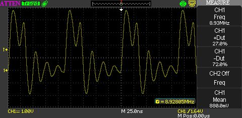
Compiling the above code and executing the application results in the following output when the oscilloscope is connection to GPIO18:
Raspberry Pi GPIO Output
It is necessary to review the documents in the resources section of this post in order to fully understand the theory behind this application.
And now it is time to take on some more complex topics.
This year has been busy and after the heavy workload at the start of the year April was a time for some much needed R&R. Time to break out the camera and explore a little of Yorkshire. During the month I took about 1,300 photographs storing both the raw sensor data and a high quality JPG image. This leaves me with a whole series of files with names like DSC_0001.nef and a corresponding JPG file DSC_0001.jpg. These names are not really descriptive of the contents of the image. Renaming the files is easy but I also need to guarantee that the link between the raw file and the JPG file is retained.
This project is trivial but I have decided to present this as I could not find any software which would do what I needed. Being a Software Engineer I decided to turn to Visual Studio and solve the problem myself.
The project files and binary are available for download (see the conclusion at the end of this article).
Image File Renamer
So the project brief is:
Rename all of the files in a directory with a specific root file name
Add a sequence number to the file name
If there is a raw file and a JPG file with the same source root file name then make sure that the two files have the same destination root file name
Should be simple enough to achieve with a small command line program.
Parsing the Command Line
First this we need to do is to find out what the user wants the application to do. In order to achieve this we need to parse the command line.
Parsing the command line is a simple task and I have written classes to do this many times in the past but recently I have come across the CommandLineParser library on CodePlex. This library is powerful and performs many of the common command line parsing tasks for you. All you need to do is provide a class with properties decorated by appropriate attributes (more on that later).
Installation is easy. Start Visual Studio and create a new C# Windows console line project. Next Open the Package Manager console (Tools -> NuGet Package Manager -> Package Manager Console) and enter the command Install-Package CommandLineParser. A few seconds later the package will have bee downloaded and added to the project. All we need to do now is use it.
The two obvious options which are needed for this application to work are the new name to be used as the root of the file name and the directory which contains the source files. These two options are represented by two properties in the options class. The code for this is as follows:
using CommandLine;
using CommandLine.Text;

namespace PhotoRenamer
{
    /// <summary>
    /// Class to parse and hold the command line options.
    /// </summary>
    class Options
    {
        /// <summary>
        /// Location of the source files.
        /// </summary>
        [Option('d', "directory", DefaultValue = ".", HelpText = "Directory containing files to be renamed (default = .)")]
        public string SourceDirectory { get; set; }

        /// <summary>
        /// New source name for the files.
        /// </summary>
        [Option('n', "name", Required = true, HelpText = "Root of the new file name.")]
        public string Name { get; set; }

        [ParserState]
        public IParserState LastParserState { get; set; }

        /// <summary>
        /// Build up the usage text.
        /// </summary>
        /// <returns>Options string</returns>
        [HelpOption]
        public string GetUsage()
        {
            return HelpText.AutoBuild(this, (HelpText current) => HelpText.DefaultParsingErrorsHandler(this, current));
        }
    }
}
As you can see, the properties within the class which represent the two command line options are decorated by an Option attribute. The attribute informs the CommandLineParser how it should deal with the property and the name and type of option it should expect.
The class is set up by creating a new instance of the Options class and executing the following code:
var options = new Options();
try
{
    if (CommandLine.Parser.Default.ParseArguments(args, options))
    {
        // Your application logic goes here.
    }
}
catch (Exception ex)
{
    Console.WriteLine(options.GetUsage());
}
This will parse the command line and set the properties accordingly. An exception will be thrown if there is a problem parsing the command line or if any of the mandatory options are not present.
The main application logic will create a list of all of the JPG files in a directory, rename the file and then look for an associated raw image file. If the raw image file exists then it is also renamed using the same root file name and sequence number. The source code is present here for completeness:
using System;
using System.IO;

namespace PhotoRenamer
{
    class Program
    {
        static void Main(string[] args)
        {
            var options = new Options();
            try
            {
                if (CommandLine.Parser.Default.ParseArguments(args, options))
                {
                    if (options.Verbose)
                    {
                        Console.WriteLine("Directory: {0}", options.SourceDirectory);
                        Console.WriteLine("Root name: {0}", options.Name);
                    }

                    if (Directory.Exists(options.SourceDirectory))
                    {
                        try
                        {
                            string[] files = Directory.GetFiles(options.SourceDirectory);
                            int sequenceNumber = 1;
                            int filesProcessed = 0;
                            string jpgExtension = string.Format(".{0}", options.JPGExtension.ToLower());
                            string rawExtension = string.Format(".{0}", options.RawExtension.ToLower());
                            foreach (string file in files)
                            {
                                if (Path.GetExtension(file).ToLower().Equals(jpgExtension))
                                {
                                    string newRootFileName = string.Format("{0}\\{1} {2:0000}", options.SourceDirectory, options.Name, sequenceNumber++);
                                    string jpgFileName = string.Format("{0}{1}", newRootFileName, jpgExtension);

                                    if (options.Verbose)
                                    {
                                        Console.WriteLine("Renaming file {0} to {1}", file, jpgFileName);
                                    }
                                    File.Move(file, jpgFileName);
                                    filesProcessed++;
                                    string sourceNEFFileName = string.Format("{0}\\{1}{2}", Path.GetDirectoryName(file), Path.GetFileNameWithoutExtension(file), rawExtension);
                                    if (File.Exists(sourceNEFFileName))
                                    {
                                        string newNEFFileName = string.Format("{0}{1}", newRootFileName, rawExtension);
                                        if (options.Verbose)
                                        {
                                            Console.WriteLine("Renaming file {0} to {1}", sourceNEFFileName, newNEFFileName);
                                        }
                                        File.Move(sourceNEFFileName, newNEFFileName);
                                        filesProcessed++;
                                    }
                                }
                            }
                            Console.WriteLine("{0} Files processed.", filesProcessed);
                        }
                        catch (Exception e)
                        {
                            Console.WriteLine(e.Message);
                        }
                    }
                    else
                    {
                        Console.WriteLine("Directory '{0}' does not exist.", options.SourceDirectory);
                    }
                }
            }
            catch (Exception ex)
            {
                Console.WriteLine(options.GetUsage());
            }
        }
    }
}
Three additional properties have been added to the Options class, two to support different raw and JPG file name extensions and a final option to put the application into verbose mode.
Conclusion
This application provides a simple methods of renaming image files keeping the link between the original raw and JPG files. The source code and compiled binary can be downloaded and used on a royalty free basis.
The source code and application are provided as is and no warranty is provided.
This post was supposed to be about controlling an LED panel using SPI on the STM32. It soon became apparent that SPI on the STM32 was a topic of it’s own and so the hardware component of the post, the LED panel, will have to wait for another day.
In this post we will aim to achieve the following:
Use SysTick to trigger regular events
Send data over SPI by polling
Use interrupts to send data by SPI
Combine SPI and DMA to send data over SPI
So let’s start with the trigger/heartbeat.
Heartbeat
The heartbeat will allow us to perform tasks at regular intervals, say 1ms, and by toggling a pin we can also determine if the processor is still “alive”.
For a simple heartbeat we can use the SysTick timer. This built in timer can be configured to generate an interrupt. The handler has it’s own entry in the interrupt vector table. It is theoretically possible to calibrate this timer to trigger at an accurate period. For the purpose of this problem we will not really need high accuracy and so will simply turn on the timer.
Setting this timer running requires only two lines of code, encapsulating this into an initialisation method gives us the following:
//
//    Initialise SysTick.
//
void InitialiseSysTick()
{
    RCC_ClocksTypeDef RCC_Clocks;
    //
    //    Setup the system tick for the heartbeat.
    //
    RCC_GetClocksFreq(&RCC_Clocks);
    SysTick_Config(RCC_Clocks.HCLK_Frequency / 1000);
}
The SysTick_Config method sets up the SysTick timer. The timer works by loading the counter with a Load value. The counter then starts to count down from the load value each tick of the clock. When the counter reaches zero it is reloaded and the whole process starts again. It is possible to generate an interrupt (SysTick_Handler) when the counter reaches zero.
The expression RCC_Clocks.HCLK_Frequency / 1000 is the counter reload value. It is important to note that the reload value is a 24-bit unsigned long and so this has a maximum value of 0xffffff. In this case the load value is 0x29040, well within the specified range. This value will give 1000 interrupts per second, i.e. an interrupt every 1ms.
Now we have a 1ms interrupt we need to determine if this interrupt is being triggered. The simplest way of doing this is to toggle one of the GPIO pins. First thing to do is to select a pin and then initialise the port. Selecting PA1 we can modify the InitialiseSysTick code above to the following:
The next task is to add the SysTick interrupt handler. Opening the startup_stm32f4xx.c file you will find the following line:
#pragma weak SysTick_Handler = Default_Handler
This statement defines the SysTick_Handler and points the handler to the Default_Handler. The weak attribute allows the developer to override this handler and provide their own interrupt handler. In our case we want the handler to toggle PA1. This gives the following code:
//
//    System tick handler.
//
void SysTick_Handler(void)
{
    //
    //    Generate a heartbeat.
    //
    GPIOA->ODR ^= GPIO_Pin_1;
}
All of the above code is placed in a file SysTick.c and an appropriate header file created. Our main program file is:
#include "SysTick.h"

//
//    Initialise the system.
//
void Initialise()
{
    InitialiseSysTick();
}

//
//    Main program loop.
//
int main()
{
    Initialise();
    while (1);
}
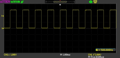
Putting this into a project, compiling and running results in the following output on the oscilloscope:
500Hz Square Wave
As you can see, we have a 500Hz square wave indicating that PA1 is being toggled 1,000 times per second.
Polled SPI
Polled SPI will use the various registers associated with the SPI feature to determine if the SPI data transmission has completed. You can also use interrupts, a subject we will come to later.
The first things we need to do is to configure the pins required to support SPI. For conventional SPI we need four pins:
MOSI (PA7)
MISO (PA6)
SCLK (PA5)
Chip select (PE6)
One change we will make is to move the heartbeat from Port A to Port E (PE5) and keep Port A for the SPI function. Abstracting the GPIO initialisation out to it’s own files gives the following header file:
//
//    Include file for the GPIO methods.
//
//    Copyright 2014 Mark Stevens
//
#include "stm32f4xx_rcc.h"
#include <stm32f4xx_gpio.h>


#ifndef _SPI_H_
#define _SPI_H_

#ifdef __cplusplus
extern "C"
{
#endif

void InitialiseGPIO();

#ifdef __cplusplus
}
#endif

#endif
Calling the InitialiseGPIO method sets up Port A for SPI and Port E for general IO.
The next step is to initialise the SPI port:
Clock is idle low
Data is sampled on the rising edge
SPI Master
8 data bits
MSB transmitted first
Clock prescalar 256 (slowest clock possible)
Coding this into an initialisation method gives:
//
//    SPI methods.
//
//    Copyright 2014 Mark Stevens
//
#include "spi.h"

//
//    Initialise SPI
//
void InitialiseSPI(void)
{
    SPI_InitTypeDef SPI_InitStruct;
    //
    //     Connect SPI1 pins to SPI alternate function.
    //
    GPIO_PinAFConfig(GPIOA, GPIO_PinSource5, GPIO_AF_SPI1);
    GPIO_PinAFConfig(GPIOA, GPIO_PinSource6, GPIO_AF_SPI1);
    GPIO_PinAFConfig(GPIOA, GPIO_PinSource7, GPIO_AF_SPI1);
    //
    //    Set PE6 high as we will be using active low for the
    //    device select.
    //
    GPIOE->BSRRL |= GPIO_Pin_6;
    //
    //     Enable the SPI peripheral clock.
    //
    RCC_APB2PeriphClockCmd(RCC_APB2Periph_SPI1, ENABLE);

    //
    //    Configure SPI1 in Mode 0:
    //        CPOL = 0 --> clock is low when idle
    //        CPHA = 0 --> data is sampled at the first edge
    //
    //    SPI Master mode, 8 bits of data, clock prescalar is 256, MSB is
    //    transmitted first.
    //
    SPI_InitStruct.SPI_Direction = SPI_Direction_2Lines_FullDuplex;
    SPI_InitStruct.SPI_Mode = SPI_Mode_Master;
    SPI_InitStruct.SPI_DataSize = SPI_DataSize_8b;
    SPI_InitStruct.SPI_CPOL = SPI_CPOL_Low;
    SPI_InitStruct.SPI_CPHA = SPI_CPHA_1Edge;
    SPI_InitStruct.SPI_NSS = SPI_NSS_Soft | SPI_NSSInternalSoft_Set;
    SPI_InitStruct.SPI_BaudRatePrescaler = SPI_BaudRatePrescaler_256;
    SPI_InitStruct.SPI_FirstBit = SPI_FirstBit_MSB;
    SPI_Init(SPI1, &SPI_InitStruct);
    //
    //    Enable SPI.
    //
    SPI_Cmd(SPI1, ENABLE);
}
As already noted, this first version of the SPI method will poll the SPI registers in order to determine the state of the SPI bus. The general algorithm is:
Set the data register to the byte to be transmitted
Wait for data transmission on MOSI to complete
Wait for data reception on MISO to complete
Wait until SPI is no longer busy
Transfer the received data from the data register
Translating to C gives the following method:
//
//    Transmit and receive a single byte of data.
//
uint8_t SPISend(uint8_t data)
{
    //
    //    Setting the Data Register (DR) transmits the byte of data on MOSI.
    //
    SPI1->DR = data;
    //
    //    Wait until the data has been transmitted.
    //
    while (!(SPI1->SR & SPI_I2S_FLAG_TXE));
    //
    //    Wait for any data on MISO pin to be received.
    //
    while (!(SPI1->SR & SPI_I2S_FLAG_RXNE));
    //
    //    All data transmitted/received but SPI may be busy so wait until done.
    //
    while (SPI1->SR & SPI_I2S_FLAG_BSY);
    //
    //    Return the data received on MISO pin.
    //
    return(SPI1->DR);
}
Before we move on to the main program we need to remember to change the SysTick_Handler and initialisation method to take into consideration the changes we have made to the initialisation of the GPIO ports and the movement of the heartbeat to Port E. The SysTick.c becomes:
//
//    SysTick methods.
//
//    Copyright 2014 Mark Stevens
//
#include "stm32f4xx_rcc.h"
#include "stm32f4xx_gpio.h"
#include "system_stm32f4xx.h"

//
//    Initialise SysTick.
//
void InitialiseSysTick()
{
    RCC_ClocksTypeDef RCC_Clocks;
    //
    //    Setup the system tick for the heartbeat.
    //
    RCC_GetClocksFreq(&RCC_Clocks);
    SysTick_Config(RCC_Clocks.HCLK_Frequency / 1000);
}

//
//    System tick handler.
//
void SysTick_Handler(void)
{
    //
    //    Generate a heartbeat.
    //
    GPIOE->ODR ^= GPIO_Pin_5;
}
The last thing to do is to modify the main program file to call the appropriate initialisation methods and then transmit the data.
//
// LED Panel - Main program and associated methods.
//
// Copyright 2014 Mark Stevens
//
#include "SPI.h"
#include "GPIO.h"
#include "SysTick.h"
#include <stm32f4xx_gpio.h>
//
// Initialise the system.
//
void Initialise()
{
InitialiseGPIO();
InitialiseSPI();
InitialiseSysTick();
}
//
// Main program loop.
//
int main()
{
Initialise();
while (1)
{
GPIOE->BSRRH |= GPIO_Pin_6; // Set PE6 (Chip Select) low
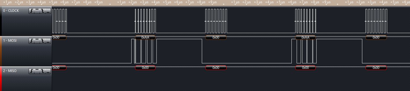
SPISend(0xAA); // Transmit data
SPISend(0x00); // Transmit dummy byte and receive data
GPIOE->BSRRL |= GPIO_Pin_6; // set PE6 (Chip Select) high
}
}
Compiling the above code and deploying it to the STM32 Discovery board generated the following output on the logic analyser:
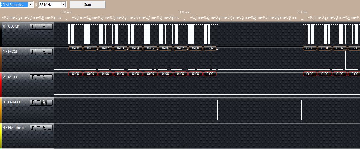
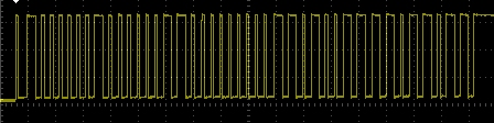
Polled SPI
A low clock speed is chosen for the SPI bus as it helps to eliminate the impact of interference from stay signals, long leads etc. Once the system is working at a low clock speed, the prescalar can be changed and the speed increased gradually until we determine the maximum rate at which data can be transmitted reliably.
The main program loop above contains two calls to the SPISend method. The first transmits the data we want top send to the slave device, the second call sends dummy data. This would allow the slave module to send a single byte response.
Interrupt Driven SPI
The final aim of this project is to be able to send data to an LED Panel using SPI. The panel itself is not required to send data back to the application. The modifications made here will take that into consideration. The following changes will be made:
Transmit only, no data will be received
Interrupt driven
Heartbeat will kick off the transmission of the data
Transmit a buffer of data (more than a single byte)
The first modification to be made is to the SPI configuration. Change the SPI_InitStruct setup to use a single Tx line and add code to configure the SPI interrupt priority:
This application will be sending a buffer of data rather than a repeated byte so we need to add somewhere to store the data. Adding the following to the SPI.c file gives us some storage:
//
//    Storage for the SPI data.
//
uint8_t buffer[SPI_BUFFER_LENGTH];
int bufferIndex = 0;
And adding the following to the SPI.h header file allows the storage to be accessible from other modules:
//
//    SPI related constants.
//
#define SPI_BUFFER_LENGTH        10

//
//    Data storage for the SPI methods.
//
uint8_t buffer[SPI_BUFFER_LENGTH];
int bufferIndex;
Ensure that the code is within the extern “C” statement.
The final bit of the puzzle is the addition of the interrupt capability. The method chosen is to configure the SPI bus and leave SPI turned on but initially have the SPI interrupts turned off. The SysTick_Handler will act as the trigger for the SPI communication starting the communication by setting up the initial conditions and turning on the SPI interrupt. The SPI interrupt handler will take over from there. Modifying the SysTick_Handler we get:
//
//    System tick handler.
//
void SysTick_Handler(void)
{
    //
    //    Generate a heartbeat.
    //
    GPIOE->ODR ^= GPIO_Pin_5;
    //
    //    If we are about to generate a rising edge on the heartbeat
    //    we are ready to start SPI data transmission.
    //
    if (GPIOE->ODR & GPIO_Pin_5)
    {
        GPIOE->BSRRH |= GPIO_Pin_6;
        bufferIndex = 0;
        SPI_I2S_ITConfig(SPI1, SPI_I2S_IT_TXE, ENABLE);
    }
}
This code starts the SPI transmission on the rising edge of the heartbeat pulse. Note also that this interrupt handler is responsible for setting the chip select line.
The final bit of the puzzle is the SPI interrupt handler itself.
//
//    Process the interrupts for SPI1.
//
void SPI1_IRQHandler()
{
    //
    //    If TX buffer is empty then transmit the next byte.
    //
    if (SPI1->SR & SPI_I2S_FLAG_TXE)
    {
        if (bufferIndex < SPI_BUFFER_LENGTH)
        {
            SPI1->DR = buffer[bufferIndex++];
        }
    }
    //
    //    If SPI is not busy then we have finished sending data
    //    so turn off this interrupt.
    //
    if (!(SPI1->SR & SPI_I2S_FLAG_BSY))
    {
        SPI_I2S_ITConfig(SPI1, SPI_I2S_IT_TXE, DISABLE);
        GPIOE->BSRRL |= GPIO_Pin_6;
    }
    //
    //    Clear the interrupt pending bit otherwise this interrupt
    //    will be regenerated.
    //
    SPI_I2S_ClearITPendingBit(SPI1, SPI_I2S_IT_TXE);
}
Two key points to notice in this interrupt handler when the end of data buffer has been reached and SPI is no longer busy:
Chip select is set to high
Interrupts are disabled
The last line of this interrupt handler clears the SPI interrupt pending bit to prevent this handler being called again as soon as it exits.
One final modification to be made is to the main program loop. This is no longer required to control the transmission of the data but we will need to setup the contents of the data buffer:
//
//    Main program loop.
//
int main()
{
    Initialise();
    //
    //    Fill the SPI buffer with data.
    //
    int index;
    for (index = 0; index < SPI_BUFFER_LENGTH; index++)
    {
        buffer[index] = index;
    }
    //
    //    Main program loop.
    //
    while (1);
}
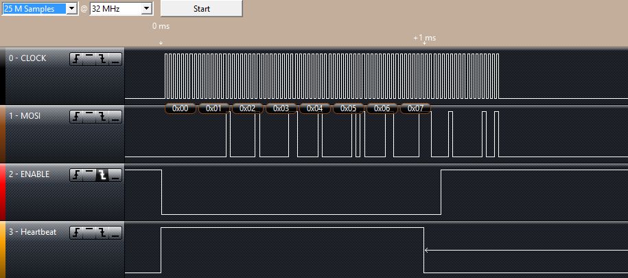
Putting all this together, compiling, deploying gives the following output on the logic analyser:
Buffered SPI With Heartbeat
SPI and DMA
The transition from polled SPI to interrupt driven SPI has so far reduced the load on the microcontroller but the STM32 has one final trick we can use, DMA (Direct Memory Access). DMA allows the various peripherals (of which SPI is one) to directly access the memory used for data storage/retrieval. By doing this the peripheral can operate autonomously until it has run out of data to process.
Remember the following in the SPI interrupt handler above:
if (bufferIndex < SPI_BUFFER_LENGTH)
{
    SPI1->DR = buffer[bufferIndex++];
}
This is required as the SPI peripheral generates an interrupt each time it has transmitted a byte of data and the buffer is empty. With DMA we can hand the SPI peripheral a block of data and tell it to transmit all of the data and simply tell us when the transmission has completed. This means we only receive one interrupt at the end of transmission rather than the 10 we receive for the above scenario.
First thing to do is to modify the InitialiseSPI method to configure the SPI peripheral to use DMA:
//
//    Initialise SPI
//
void InitialiseSPI()
{
    SPI_InitTypeDef SPI_InitStruct;
    NVIC_InitTypeDef NVIC_InitStructure;
    DMA_InitTypeDef DMA_InitStructure;
    //
    //     Connect SPI1 pins to SPI alternate function.
    //
    GPIO_PinAFConfig(GPIOA, GPIO_PinSource5, GPIO_AF_SPI1);
    GPIO_PinAFConfig(GPIOA, GPIO_PinSource6, GPIO_AF_SPI1);
    GPIO_PinAFConfig(GPIOA, GPIO_PinSource7, GPIO_AF_SPI1);
    //
    //    Set PE6 high as we will be using active low for the
    //    device select.
    //
    GPIOE->BSRRL |= GPIO_Pin_6;
    //
    //     Enable the SPI peripheral clock.
    //
    RCC_APB2PeriphClockCmd(RCC_APB2Periph_SPI1, ENABLE);
    //
    //    Configure SPI1 in Mode 0:
    //        CPOL = 0 --> clock is low when idle
    //        CPHA = 0 --> data is sampled at the first edge
    //
    //    SPI Master mode, 8 bits of data, clock prescalar is 128, MSB is
    //    transmitted first.
    //
    SPI_InitStruct.SPI_Direction = SPI_Direction_1Line_Tx;// SPI_Direction_2Lines_FullDuplex;
    SPI_InitStruct.SPI_Mode = SPI_Mode_Master;
    SPI_InitStruct.SPI_DataSize = SPI_DataSize_8b;
    SPI_InitStruct.SPI_CPOL = SPI_CPOL_Low;
    SPI_InitStruct.SPI_CPHA = SPI_CPHA_1Edge;
    SPI_InitStruct.SPI_NSS = SPI_NSS_Soft | SPI_NSSInternalSoft_Set;
    SPI_InitStruct.SPI_BaudRatePrescaler = SPI_BaudRatePrescaler_256;
    SPI_InitStruct.SPI_FirstBit = SPI_FirstBit_MSB;
    SPI_Init(SPI1, &SPI_InitStruct);
    //
    //    Configure the DMA controller
    //
    RCC_AHB1PeriphClockCmd(RCC_AHB1Periph_DMA2, ENABLE);
    DMA_StructInit(&DMA_InitStructure);
    DMA_InitStructure.DMA_Channel = DMA_Channel_3;
    DMA_InitStructure.DMA_PeripheralBaseAddr  = (uint32_t) &(SPI1->DR);
    DMA_InitStructure.DMA_Memory0BaseAddr  = (uint32_t) &buffer;
    DMA_InitStructure.DMA_DIR = DMA_DIR_MemoryToPeripheral;
    DMA_InitStructure.DMA_BufferSize  = SPI_BUFFER_LENGTH;
    DMA_InitStructure.DMA_PeripheralInc  = DMA_PeripheralInc_Disable;
    DMA_InitStructure.DMA_MemoryInc  = DMA_MemoryInc_Enable;
    DMA_InitStructure.DMA_PeripheralDataSize  = DMA_PeripheralDataSize_Byte;
    DMA_InitStructure.DMA_MemoryDataSize  = DMA_MemoryDataSize_Byte;
    DMA_InitStructure.DMA_Mode  = DMA_Mode_Normal;
    DMA_InitStructure.DMA_Priority  = DMA_Priority_High;
    DMA_InitStructure.DMA_FIFOMode  = DMA_FIFOMode_Disable;
    DMA_Init(DMA2_Stream5, &DMA_InitStructure);
    DMA_ITConfig(DMA2_Stream5, DMA_IT_TC, ENABLE);

    NVIC_InitStructure.NVIC_IRQChannel = DMA2_Stream5_IRQn;
    NVIC_InitStructure.NVIC_IRQChannelPreemptionPriority = 0;
    NVIC_InitStructure.NVIC_IRQChannelSubPriority = 1;
    NVIC_InitStructure.NVIC_IRQChannelCmd = ENABLE;
    NVIC_Init(&NVIC_InitStructure);
    //
    //    Enable SPI.
    //
    SPI_Cmd(SPI1, ENABLE);
}
The DMA controller is configured for memory to peripheral data transfer (from the buffer to the SPI->DR register). The pointer into memory is incremented after each transmission but the destination pointer (SPI->DR) remains fixed. The system will use DMA2, channel 3, stream 5. The choice of the DMA peripheral, stream and channel has some freedom but is constrained by the choice of peripheral. The list of allowed choices can be found in the STM32 Programmers Reference. As we are using SPI1 we are forced to use DMA2, channel 3 but we can choose between streams 3 and 5.
The next thing to do is to add a new interrupt handler for the DMA completion interrupt:
//
//    SPI DMA handler.
//
void DMA2_Stream5_IRQHandler()
{
    //
    //     Test if DMA Stream Transfer Complete interrupt
    //
    if (DMA_GetITStatus(DMA2_Stream5, DMA_IT_TCIF5) == SET)
    {
        DMA_ClearITPendingBit(DMA2_Stream5, DMA_IT_TCIF5);
        //
        //    The following is required to ensure that the chip select is not
        //    changed while data is still being transmitted.
        //
        while (SPI_I2S_GetFlagStatus(SPI1, SPI_I2S_FLAG_BSY) == SET);
        //
        //    Now set chip select to high.
        //
        GPIOE->BSRRL |= GPIO_Pin_6;
    }
}
Make a note of the while loop in the middle of the if statement. We will come back to this later.
The final piece of work is to modify the SysTick_Handler method:
//
//    System tick handler.
//
void SysTick_Handler(void)
{
    //
    //    Generate a heartbeat.
    //
    GPIOE->ODR ^= GPIO_Pin_5;
    //
    //    If we are about to generate a rising edge on the heartbeat
    //    we are ready to start SPI data transmission.
    //
    if (GPIOE->ODR & GPIO_Pin_5)
    {
        GPIOE->BSRRH |= GPIO_Pin_6;
        DMA2_Stream5->M0AR = (uint32_t) &buffer;
        DMA_Cmd(DMA2_Stream5, ENABLE);
        SPI_I2S_DMACmd(SPI1, SPI_I2S_DMAReq_Tx, ENABLE);
    }
}
As with the previous interrupt example, this method starts the transfer process.
Putting this together in a project, compiling and deploying gives the following output on the logic analyser:
Multiple DMA SPI Transfers
Remember the while loop above. This is necessary as the DMA transfer complete interrupt is generated as soon as the data has been transferred from memory to the SPI peripheral. This does not necessarily mean that the data has been transferred to the slave device connected to the SPI bus. If we did not have the loop in the handler to check that the transfer had completed we could end up in a situation where the chip select line to taken high before data transfer has completed. This is verified by the following trace on the logic analyser:
Enable Asserting Before Transfer Complete
Note how chip select goes high when we still have nearly a full byte of data to transmit.
Conclusion
What started out as an investigation into the control of an LED panel turned into a marathon investigation into SPI on the STM32. This post has presented three different methods for controlling data transfer over SPI each having its own merits. The source code for the CooCox projects can be downloaded here:
A remote control which can only generate a signal when initially powered up is of limited use. The addition of a switch will allow the user to determine when the camera is triggered.
Adding a Button
The initial versions of the infra-red remote control for the Nikon D70 which have been discussed so far are limited in that the control sequence is transmitted when the STM8S starts and never again until the next time the STM8S is restarted/reset. Adding a button to the remote control will allow the user to select when the control sequence is transmitted.
One of the main problems with switches is that they are subject to switch bounce. You can see an example of this in the post regarding External Interrupts on the STM8S. There are two approaches to switch debouncing, software and hardware. The button on the infra-red remote control will be triggering a sequence of pulses which will typically last several milliseconds. This means that it lends itself to software debouncing using a simple state machine.
The state machine will put the infra-red remote control into two states, waiting for user input and running. When waiting for user input the interrupt handler for the switch will accept user input. When in the running mode the system will be generating the infra-red output for the camera and it will ignore any input from the switch. At the end of the infra-red sequence the switch input will be re-enabled.
So much for the theory, lets have a look at the code. The first thing which the application will need to do is to setup the appropriate pin as an interrupt port:
//--------------------------------------------------------------------------------
//
//  Now set up the ports.
//
//  PD3 - IR Pulse signal.
//  PD4 - Input pin indicating that the user wishes to trigger the camera.
//
void SetupPorts()
{
    PD_ODR = 0;             //  All pins are turned off.
    //
    //  PD3 is the output for the IR control.
    //
    PD_DDR_DDR3 = 1;
    PD_CR1_C13 = 1;
    PD_CR2_C23 = 1;
    //
    //  Now configure the input pin.
    //
    PD_DDR_DDR4 = 0;        //  PD4 is input.
    PD_CR1_C14 = 1;         //  PD4 is floating input.
    PD_CR2_C24 = 1;
    //
    //  Set up the interrupt.
    //
    EXTI_CR1_PDIS = 1;      //  Interrupt on rising edge.
    EXTI_CR2_TLIS = 1;      //  Rising edge only.
}
The modifications to the SetupPorts method keeps the infra-red output on PD3 but adds an input on PD4 with a rising edge interrupt.
The next step is to deal with the interrupt on PD4. Here we need to work out if we are waiting for an interrupt and if we are then the application needs to start the generation of the infra-red signal. If we are not waiting for a button press then we should ignore the user request as it is likely to be a result of switch bounce. The code starts to look like this:
//--------------------------------------------------------------------------------
//
//  Process the interrupt generated by the pressing of the button.
//
//  This ISR makes the assumption that we only have on incoming interrupt on Port D.
//
#pragma vector = 8
__interrupt void EXTI_PORTD_IRQHandler(void)
{
    if (_currentState != STATE_RUNNING)
    {
        //
        //  Set everything up ready for the timers.
        //

        //  TODO!

        //
        //  Now we have everything ready we need to force the Timer 2 counters to
        //  reload and enable Timers 1 & 2.
        //
        TIM2_CR1_URS = 1;
        TIM2_EGR_UG = 1;
        TIM1_CR1_CEN = 1;
        TIM2_CR1_CEN = 1;
    }
}
The exact code required for setting up the timer will be revealed following the EEPROM section of this post.
Using EEPROM
In the post Storing Data in the EEPROM on the STM8S we saw how we could save data into the EEPROM of the STM8S for later retrieval. The data used in the example should look familiar if you have been following this series on the Nikon D70 Remote Control as it is the timing and signal data which triggers the Nikon D70.
The first thing we should do is to modify the order in which the data is written into the EEPROM. In the above post, the timing data is written into the EEPROM low byte followed by high byte. By swapping the order we can store the data in the order required by the interrupt for Timer 2. So the first task is to modify the application which wrote and verified the timing information to the following:
//
//  Write a series of bytes to the EEPROM of the STM8S105C6 and then
//  verify that the data has been written correctly.
//
//  This software is provided under the CC BY-SA 3.0 licence.  A
//  copy of this licence can be found at:
//
//  http://creativecommons.org/licenses/by-sa/3.0/legalcode
//
#if defined DISCOVERY
    #include <iostm8S105c6.h>
#else
    #include <iostm8s103f3.h>
#endif

//
//  Data to write into the EEPROM.
//
unsigned int _pulseLength[] = { 2000U, 27830U, 400U, 1580U, 400U, 3580U, 400U };
unsigned char _onOrOff[] =    {   1,      0,     1,     0,    1,     0,    1 };
char numberOfValues = 7;

//--------------------------------------------------------------------------------
//
//  Write the default values into EEPROM.
//
void SetDefaultValues()
{
    //
    //  Check if the EEPROM is write-protected.  If it is then unlock the EEPROM.
    //
    if (FLASH_IAPSR_DUL == 0)
    {
        FLASH_DUKR = 0xae;
        FLASH_DUKR = 0x56;
    }
    //
    //  Write the data to the EEPROM.
    //
    char *address = (char *) 0x4000;        //  EEPROM base address.
    *address++ = (char) numberOfValues;
    for (int index = 0; index < numberOfValues; index++)
    {
        *address++ = (char) ((_pulseLength[index] >> 8) & 0xff);
        *address++ = (char) (_pulseLength[index] & 0xff);
        *address++ = _onOrOff[index];
    }
    //
    //  Now write protect the EEPROM.
    //
    FLASH_IAPSR_DUL = 0;
}

//--------------------------------------------------------------------------------
//
//  Verify that the data in the EEPROM is the same as the data we
//  wrote originally.
//
void VerifyEEPROMData()
{
    PD_ODR_ODR2 = 1;            //  Checking the data
    PD_ODR_ODR3 = 0;            //  No errors.
    //
    char *address = (char *) 0x4000;        //  EEPROM base address.
    if (*address++ != numberOfValues)
    {
        PD_ODR_ODR3 = 1;
    }
    else
    {
        for (int index = 0; index < numberOfValues; index++)
        {
            unsigned int value = (*address++ << 8);
            value += *address++;
            if (value != _pulseLength[index])
            {
                PD_ODR_ODR3 = 1;
            }
            if (*address++ != _onOrOff[index])
            {
                PD_ODR_ODR3 = 1;
            }
        }
    }
    PD_ODR_ODR2 = 0;        // Finished processing.
}

//--------------------------------------------------------------------------------
//
//  Setup port D for data output.
//
void SetupPorts()
{
    //
    //  Initialise Port D.
    //
    PD_ODR = 0;             //  All pins are turned off.
    PD_DDR = 0xff;          //  All bits are output.
    PD_CR1 = 0xff;          //  All pins are Push-Pull mode.
    PD_CR2 = 0xff;          //  Pins can run up to 10 MHz.
}

//--------------------------------------------------------------------------------
//
//  Main program loop.
//
void main()
{
    SetupPorts();
    SetDefaultValues();
    VerifyEEPROMData();
}
Create a new project for the above and execute the program on the STM8S Discovery board. This should set up the timing data ready for use to use.
Using the EEPROM Data
The above application has been tailored to write the byte data into the EEPROM in the order in which the bytes are required by the remote control application. Using this data should be a simple case of setting a pointer to the first byte and then consuming the bytes one after another. To do this we will need some pointers and a counter:
//
//  Define where we will be working in the EEPROM.
//
#define EEPROM_BASE_ADDRESS         0x4000
#define EEPROM_INITIAL_OFFSET       0x0000
#define EEPROM_DATA_START           (EEPROM_BASE_ADDRESS + EEPROM_INITIAL_OFFSET)

//
//  Data ready for the pulse timer ISR's to use.
//
int _numberOfPulses = 0;
int _currentPulse = 0;
char *_pulseDataAddress = NULL;
As part of the initialisation process we will need to set the pointer and also the number of pulses we have data for:
So now we should have the initial state configured and we should revisited the button handler method. This method kicks off the timers by consuming the first three bytes of data:
//--------------------------------------------------------------------------------
//
//  Process the interrupt generated by the pressing of the button.
//
//  This ISR makes the assumption that we only have on incoming interrupt on Port D.
//
#pragma vector = 8
__interrupt void EXTI_PORTD_IRQHandler(void)
{
    if (_currentState != STATE_RUNNING)
    {
        //
        //  Set everything up ready for the timers.
        //
        _currentState = STATE_RUNNING;
        _currentPulse = 0;
        _pulseDataAddress = (char *) (EEPROM_DATA_START + 1);
        TIM2_ARRH = *_pulseDataAddress++;
        TIM2_ARRL = *_pulseDataAddress++;
        PD_ODR_ODR3 = *_pulseDataAddress++;
        //
        //  Now we have everything ready we need to force the Timer 2 counters to
        //  reload and enable Timers 1 & 2.
        //
        TIM2_CR1_URS = 1;
        TIM2_EGR_UG = 1;
        TIM1_CR1_CEN = 1;
        TIM2_CR1_CEN = 1;
    }
}
Finally, the interrupt for the Timer 2 interrupt needs to be modified in order to continue to process the data three bytes at a time until we have reached the total number of pulses:
//--------------------------------------------------------------------------------
//
//  Timer 2 Overflow handler.
//
#pragma vector = TIM2_OVR_UIF_vector
__interrupt void TIM2_UPD_OVF_IRQHandler(void)
{
    _currentPulse++;
    if (_currentPulse == _numberOfPulses)
    {
        //
        //  We have processed the pulse data so stop now.
        //
        PD_ODR_ODR3 = 0;
        TIM2_CR1_CEN = 0;
        TIM1_CR1_CEN = 0;           //  Stop Timer 1.
        _currentState = STATE_WAITING_FOR_USER;
    }
    else
    {
        TIM2_ARRH = *_pulseDataAddress++;
        TIM2_ARRL = *_pulseDataAddress++;
        PD_ODR_ODR3 = *_pulseDataAddress++;
        TIM2_CR1_URS = 1;
        TIM2_EGR_UG = 1;
    }
    TIM2_SR1_UIF = 0;               //  Reset the interrupt otherwise it will fire again straight away.
}
Conclusion
The addition of the button certainly makes the remote control more usable as the user can elect when to trigger the camera. At this stage, the EEPROM does not offer too many advantages over the use of the static data but it can allow the remote control to be fine-tuned at a later stage.
The acid test, does it still trigger the camera – Yes it does.
I considered two methods of modulating the signal:
Software implementation using a timer
Hardware implementation using PWM
The software implementation is attractive as it does not require the addition of any additional components to the circuit and hence reduces the cost of the remote control. On the downside, this requires a slightly more complex implementation and may cause some issues due to the timing of the interrupts.
Using PWM is a much simpler software solution as it only requires that the timers are setup correctly and turned on at the right time.
How Does Modulation Work?
Modulation works by combining a clock frequency (in the case of infra-red this is normally around 38KHz – 40 KHz) with a digital signal. When the digital signal is supposed to be at logic 1 then the clock signal is output rather than a stable logic level 1. When the signal is at logic level 0 then no signal is generated. The following illustrates this:
Digital signal:
Digital Signal
Clock signal:
38.4KHz Clock Signal
Combined output:
Digital Signal And Clock
In the final image above, the top trace shows the clock signal, the middle trace shows the digital signal we wish to generate and the lower trace shows the signal which should be output by the circuit.
Hardware Changes
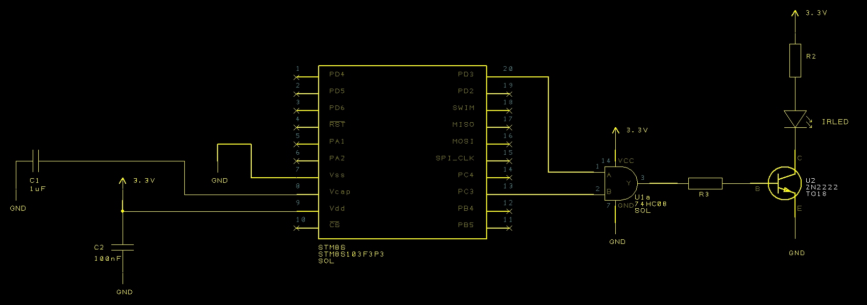
The hardware solution requires the combination of a digital signal with a PWM signal. The easiest way to do this is to use a single AND gate taking input from the digital output required and a clock signal.
Nikon Remote Circuit With Added Modulation
Searching the RS Components web site lead to a single and gate component for a small price. This would be ideal for solving this problem.
Software Changes
The software changes are minimal as we simply need to configure a timer and turning it on and off as required. We will be using Timer 1, Channel 4 configured to generate a 38.4KHz PWM signal.
Setup
A 38.4KHz signal has a peak to peak duration of 26uS The system is running at 2MHz and so we would need a count value of 52 clock pulses (with no prescalar applied). Using Timer 2, Channel 4 results in the following setup code:
//--------------------------------------------------------------------------------
//
//  Set up Timer 1, channel 4 to output a single pulse lasting 240 uS.
//
void SetupTimer1()
{
    TIM1_ARRH = 0x00;       //  Reload counter = 51
    TIM1_ARRL = 0x33;
    TIM1_PSCRH = 0;         //  Prescalar = 0 (i.e. 1)
    TIM1_PSCRL = 0;
    //
    //  Now configure Timer 1, channel 4.
    //
    TIM1_CCMR4_OC4M = 7;    //  Set up to use PWM mode 2.
    TIM1_CCER2_CC4E = 1;    //  Output is enabled.
    TIM1_CCER2_CC4P = 0;    //  Active is defined as high.
    TIM1_CCR4H = 0x00;      //  26 = 50% duty cycle (based on TIM1_ARR).
    TIM1_CCR4L = 0x1a;
    TIM1_BKR_MOE = 1;       //  Enable the main output.
}
Timer 2 Interrupt Handler
A minor change to the Timer 2 interrupt handler is required to turn off Timer 1 when the signal is no longer being generated:
//--------------------------------------------------------------------------------
//
//  Timer 2 Overflow handler.
//
#pragma vector = TIM2_OVR_UIF_vector
__interrupt void TIM2_UPD_OVF_IRQHandler(void)
{
    _currentPulse++;
    if (_currentPulse == _numberOfPulses)
    {
        //
        //  We have processed the pulse data so stop now.
        //
        PD_ODR_ODR3 = 0;
        TIM2_CR1_CEN = 0;
        TIM1_CR1_CEN = 0;           //  Stop Timer 1.
    }
    else
    {
        TIM2_ARRH = _counterHighBytes[_currentPulse];
        TIM2_ARRL = _counterLowBytes[_currentPulse];
        PD_ODR_ODR3 = _outputValue[_currentPulse];
        TIM2_CR1_URS = 1;
        TIM2_EGR_UG = 1;
    }
    TIM2_SR1_UIF = 0;               //  Reset the interrupt otherwise it will fire again straight away.
}
Main Loop
The final change is to the main program loop. This needs to start Timer 1 when the application starts to output data:
//--------------------------------------------------------------------------------
//
//  Main program loop.
//
void main()
{
    unsigned int pulseLength[] = { 2000U, 27830U, 400U, 1580U, 400U, 3580U, 400U };
    unsigned char onOrOff[] =    {   1,      0,     1,     0,    1,     0,    1 };
    PrepareCounterData(pulseLength, onOrOff, 7);
    __disable_interrupt();
    SetupTimer2();
    SetupTimer1();
    SetupOutputPorts();
    __enable_interrupt();
    PD_ODR_ODR3 = _outputValue[0];
    //
    //  Now we have everything ready we need to force the Timer 2 counters to
    //  reload and enable Timer 2.
    //
    TIM2_CR1_URS = 1;
    TIM2_EGR_UG = 1;
    TIM2_CR1_CEN = 1;
    TIM1_CR1_CEN = 1;       // Start Timer 1
    while (1)
    {
        __wait_for_interrupt();
    }
}
Conclusion
Connecting the logic analyser to the circuit will allow the examination of the three signals, namely, the digital signal required (centre trace), the clock (upper trace) and the modulated output (lower trace):
Modulated IR Signal
The solid white blocks in the clock and modulated traces show a high density of signals. Zooming in on the right hand side of the capture shows the following:
Modulated IR Signal Zoom View
As you can see, the modulated output is composed of a series of 38.4KHz clock pulses which are only generated when the digital signal should be high (logic 1). The remainder of the time the trace shows no output.
The final test is to see if this will trigger the camera, and yes, it still does.
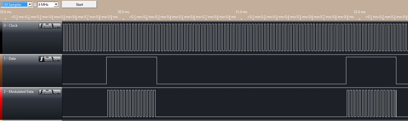
A while ago I wrote a small library for the RN-42 Bluetooth module. This small module acted as a serial port when connected to the Netduino. Times have moved on with Bluetooth 4.0 being available on the iPhone I thought I would take another look at Bluetooth.
Bluetooth Module
The Bluetooth module we will be using is the RedBear Bluetooth Mini. This little module is a Bluetooth 4.0 Low Energy (BLE) module. In it’s simplest form it offers the ability to act as a serial port for your project. This is how we will be using this module for this project.
Bluetooth Device
To test this a BLE compatible device is required. Enter the iPhone 5 and the BLE Arduino application which RedBear have thoughtfully provided. The application may be written for Arduino but it is sending simple serial commands to the Arduino. Let’s see what it is doing and if we can use this application.
Serial Port Settings
First job is to figure out the serial port settings. Scanning the source code for the Arduino I came across the following line in the setup method:
BleFirmata.begin(57600);
My guess is that this is setting up the Arduino serial port to run at 57,600 baud using standard data bits, parity and top bit settings. Time to break out the logic analyser.
Connections between the Netduino and the RedBear module is simple:
Netduino Pin
Redbear BLE Module Pin
D0 (Rx)
Tx
D1 (Tx)
Rx
3.3V
Vin
GND
GND
Additionally, the logic analyser is connected to the Rx and Tx pins of the Netduino. An Async Serial analyser was added to the two pins through the Saleae software. This analyser has an Autobaud feature. Turn this on just in case we get the baud rate incorrect.
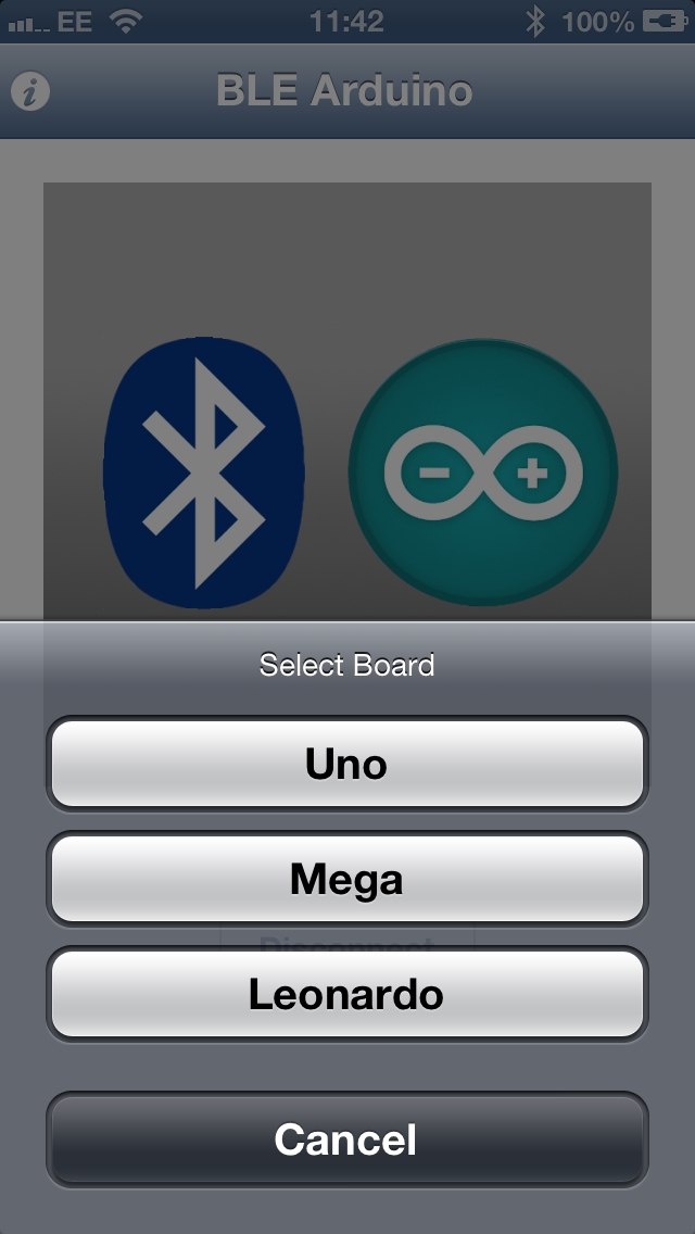
Next step is to install the BLE Arduino application on the iPhone 5. Start the application:
ReadBear BLE Software Opening Screen
Press the Click button to connect to the ReadBear module.
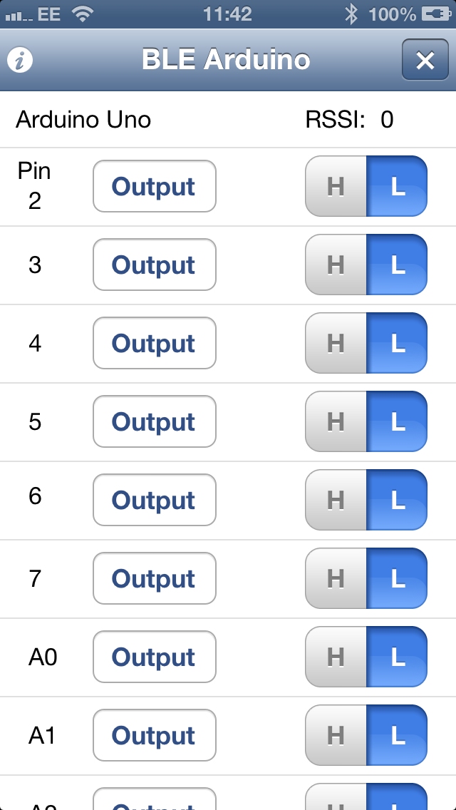
Select Arduino Board
Select the Arduino to connect to. The Arduino Uno has a similar pin out so select the Uno option.
Change a Pin Output Using BLE Software
So far there has been no output on the logic analyser. Change the state of an output pin (pressing H or L). This generates serial data:
Serial Data On the Logic Analyser
A quick check in the Async Serial analysers properties shows that the data logic analyser thinks that the data is being sent at 60,000 baud, pretty close to the 57,600 which was found in the code earlier.
Netduino Code
The next step is to try to connect some code on the Netduino to the iPhone application. The simplest application we can use simply captures the incoming data on the serial port and displays the bytes received in the debug window of Visual Studio. The following should do the trick:
public class Program
{
    const int BUFFER_SIZE = 1024;

    public static void Main()
    {
        SerialPort sp = new SerialPort("COM1", 57600, Parity.None, 8, StopBits.One);
        sp.DataReceived += sp_DataReceived;
        sp.Open();
        Thread.Sleep(Timeout.Infinite);
    }

    static void sp_DataReceived(object sender, SerialDataReceivedEventArgs e)
    {
        string str;
        str = "";
        if (e.EventType == SerialData.Chars)
        {
            int amount;
            byte[] buffer;

            buffer = new byte[BUFFER_SIZE];
            amount = ((SerialPort) sender).Read(buffer, 0, BUFFER_SIZE);
            if (amount > 0)
            {
                for (int index = 0; index < amount; index++)
                {
                    str += buffer[index].ToString();
                    str += " ";
                }
                Debug.Print("Data: " + str);
            }
        }
    }
}
Deploying the above code to my Netduino Plus 2 and running the application gives the following output:
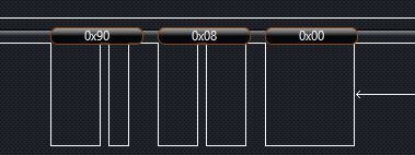
Pressing the H at the side of Pin 2 in the application generates the sequence 144 4 0. Following this up by pressing the H at the side of Pin 3 results in the sequence 144 12 0. Checking the Arduino code shows that the digital commands are prefixed by 0x90, i.e. 144.
The iPhone Application
Now that we know the iPhone and the Netduino can communicate (at least from the phone to the Netduino) let’s have a look at creating our own iPhone application. The simplest application would entail toggling a digital pin, so let’s do that. We’ll turn an LED on and off.
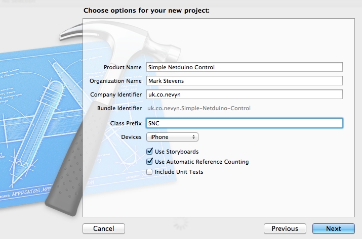
Starting XCode we will create a new project (Single View Application) for the iPhone and set the application be targeted at the iPhone only and to use Automatic Reference Counting (ARC):
New iPhone Project Options
Next we need to add the CoreBluetooth.Framework references to the application. So scroll down the frameworks and click on the + button under the Linked Frameworks section. Type bluetooth in order to search the installed frameworks.
Next, we need to add the RedBear BLE framework. I downloaded this and put it in my stored libraries. This was then added by right clicking on the Frameworks folder of the project, selecting Add Files to… and then browsing to the folder which contained the files.
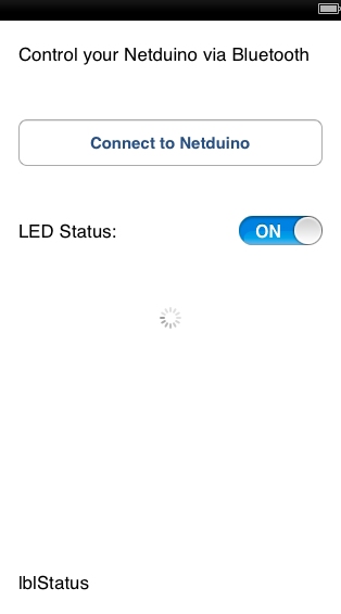
Next we head over to the Storyboard and add a few controls to our interface:
iPhone Application in XCode
Control
Description
btnConnectToNetduino
Button to connect/disconnect to/from the Netduino.
lblStatus
Label to indicate the status of the application.
lblLEDStatus
Label containing the text LED Status
swLED
Switch which is used to turn the LED on/off.
aiBusy
Indicator which shows when the application is trying to detect the Bluetooth module.
First thing to do is to connect the controls to the code in the header file for the view controller:
These definitions create the Bluetooth object and he variables required for state control.
Supporting Methods
The Connected and Disconnected methods change the interface and state variables when we have successfully connected or disconnected to/from the Bluetooth module:
//
//  Set up the interface to show that the Bluetooth module is connected
//
- (void) Connected
{
    [lblStatusMessage setText:@"Connected"];
    lblLEDStatus.hidden = false;
    swLED.hidden = false;
    [btnConnectToNetduino setTitle:@"Disconnect from Netduino" forState:UIControlStateNormal];
    btnConnectToNetduino.enabled = true;
    [self.aiBusy stopAnimating];
    mode = MODE_CONNECTED;
}

//
//  Set up the interface to show that the Bluetooth module is disconnected
//
- (void) Disconnected
{
    [lblStatusMessage setText:@"Disconnected"];
    lblLEDStatus.hidden = true;
    swLED.hidden = true;
    [btnConnectToNetduino setTitle:@"Connect to Netduino" forState:UIControlStateNormal];
    btnConnectToNetduino.enabled = true;
    [self.aiBusy stopAnimating];
    mode = MODE_DISCONNECTED;
}
Standard Methods (viewDidLoad and didReceiveMemoryWarning)
These methods are generated by default when the application is first created. For viewDidLoad we will set up the application for initial use. We will not be modifying the didReceiveMemoryWarning method in this application.
//
//  Setup the view.
//
- (void) viewDidLoad
{
    [super viewDidLoad];
    //
    //  Setup the display.
    //
    lblLEDStatus.hidden = true;
    [swLED setOn:NO];
    swLED.hidden = true;
    [lblStatusMessage setText:@"Ready"];
    self.aiBusy.hidesWhenStopped = true;
    //
    //  Create the Bluetooth objects.
    //
    ble = [[BLE alloc] init];
    [ble controlSetup:1];
    ble.delegate = self;
    //
    //  Setp the simple properties.
    //
    mode = MODE_DISCONNECTED;
}

//
//  Process the memory warning event.
//
- (void) didReceiveMemoryWarning
{
    [super didReceiveMemoryWarning];
}
The main point to note in the viewDidLoad method is that the Bluetooth object is initialised.
Button Press Event
The btnConnect_TouchUpInside event initiates the connection/disconnection of the application to/from the Bluetooth module.
//
//  User has pressed the Connect button so try to connect/disconnect from the Netduino.
//
- (IBAction) btnConnect_TouchUpInside:(UIButton *) sender
{
    if (ble.activePeripheral)
    {
        if (ble.activePeripheral.isConnected)
        {
            [[ble CM] cancelPeripheralConnection:[ble activePeripheral]];
        }
    }
    ble.peripherals = nil;
    switch (mode)
    {
        case MODE_DISCONNECTED:
            [lblStatusMessage setText:@"Connecting..."];
            [NSTimer scheduledTimerWithTimeInterval:(float) TIMEOUT_BUSY_CONNECTING target:self selector:@selector(connectionTimer:) userInfo:nil repeats:NO];
            [ble findBLEPeripherals:TIMEOUT_BLE_TIMEOUT];
            [self.aiBusy startAnimating];
            mode = MODE_CONNECTING;
            break;
        case MODE_CONNECTED:
            [lblStatusMessage setText:@"Disconnecting..."];
            [self.aiBusy startAnimating];
            mode = MODE_DISCONNECTING;
            break;
        default:
            break;
    }
    btnConnectToNetduino.enabled = false;
}
Timer
The btnConnect_TouchUpInside event starts a timer when it is trying to connect to a Bluetooth module. This timer prevents the application from locking when searching for a Bluetooth module which does not exist. The timer callback stops the search process after 3 seconds:
//
//  The timer started by the Connect button has triggered.  See if we have any
//  Bluetooth modules nearby.  If we have then connect to the first one in the
//  list.
//
-(void) connectionTimer:(NSTimer *) timer
{
    if (ble.peripherals.count > 0)
    {
        [ble connectPeripheral:[ble.peripherals objectAtIndex:0]];
    }
    else
    {
        [lblStatusMessage setText:@"Cannot find Netduino"];
        mode = MODE_DISCONNECTED;
    }
    [self.aiBusy stopAnimating];
}
Switching the LED on/off
The application assumes only one LED is connected to the Netduino. The data packet sent to the Netduino therefore contains a 1 or 0 to indicate the status of the LED:
//
//  User has changed the value of the LED.
//
- (IBAction) swLED_Changed:(UISwitch *) sender
{
    UInt8 buffer[1];
    buffer[0] = sender.isOn == YES ? 1 : 0;
    NSData *data = [[NSData alloc] initWithBytes:buffer length:1];
    [ble write:data];
}
Bluetooth Module Events
The final two events are generated by the Bluetooth library. These are fired when the module connects/disconnects to/from the module:
//
//  Connected to a Bluetooth module successfully.
//
-(void) bleDidConnect
{
    [self Connected];
}

//
//  Application has disconnected from a Bluetooth module.
//
- (void) bleDidDisconnect
{
    [self Disconnected];
}

//
//  RSSI has been updated.
//
- (void) bleDidDisconnect:(NSNumber *) rssi
{
}
Netduino Application
The final task is to modify the Netduino Application to process the data. An OutputPort is added to the application and this is connected to a digital IO pin. This pin is then turned on/off when serial data is received from the Bluetooth module:
public class Program
{
    const int BUFFER_SIZE = 1024;
    private static OutputPort led = new OutputPort(Pins.GPIO_PIN_D8, false);

    public static void Main()
    {
        SerialPort sp = new SerialPort("COM1", 57600, Parity.None, 8, StopBits.One);
        sp.DataReceived += sp_DataReceived;
        sp.Open();
        Thread.Sleep(Timeout.Infinite);
    }

    static void sp_DataReceived(object sender, SerialDataReceivedEventArgs e)
    {
        string str;
        str = "";
        if (e.EventType == SerialData.Chars)
        {
            int amount;
            byte[] buffer;

            buffer = new byte[BUFFER_SIZE];
            amount = ((SerialPort) sender).Read(buffer, 0, BUFFER_SIZE);
            if (amount > 0)
            {
                for (int index = 0; index < amount; index++)
                {
                    str += buffer[index].ToString();
                    str += "";
                }
                if (buffer[0] == 1)
                {
                    led.Write(true);
                }
                else
                {
                    led.Write(false);
                }
                Debug.Print("Data: " + str);
            }
        }
    }
}
Does it Work?
Well of course it does and here’s the video to prove it:
First we connect to the module. Once connected we can start to turn the LED on and off using the iPhone.
Conclusion
The library provided by RedBear is a great starting point for using the iPhone to communicate with a BLE module. It is simple and easy to use for this type of application. This whole experiment only took a few hours to put together an execute.
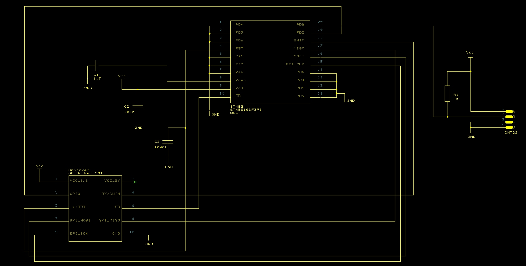
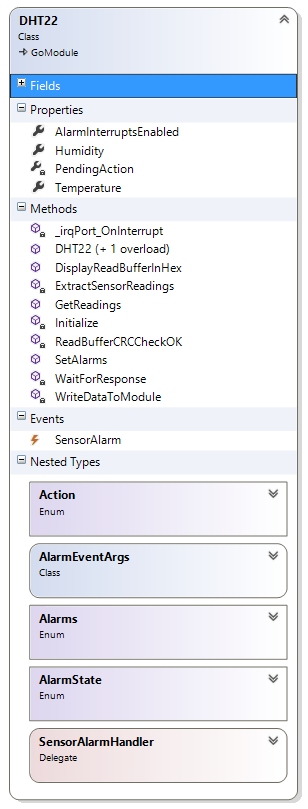
A while ago (forgive the pun), Arron Chapman and I started to collaborate on building a temperature and humidity sensor based upon the DHT22 sensor. One of the original posts discussing the module can be found here in the Netduino forums. From the very start we agreed that both the hardware and software would be open source. This post will discuss the basic hardware requirements and the software required to create a Temperature and Humidity Module for the Netduino GO!.
This post has a software bias given the relatively simple nature of the hardware being developed. Here is a flavour of what was achieved:
The design work for this module is the combined effort of Arron Chapman of Variable Labs and myself.
DHT22 Temperature and Humidity Sensor
The DHT22 is a four pin package capable of measuring temperature (+/- 0.5C) and humidity (+/- 5%). The package uses a single wire interface for communication and can be powered by 3.3-5V. The single wire protocol used is not compatible with Dallas single wire protocol.
The four pins should be connected as follows:
Pin
Connection
1
VDD (3.3-5V)
2
Data/Signal
3
Ground
4
Ground
Pin 2 (Data/Signal) should be connected to the microcontroller with a pull-up resistor to VDD.
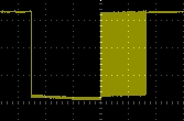
The microcontroller sends a start signal to the sensor which then responds with the data representing the temperature and humidity. The data is terminated with a check sum. The sensor can only be read at most once every 2 seconds. The trace for a full start, transmit and end signal looks like this:
The communication starts with the microcontroller sending the start signal. The microcontroller pulls the signal line low for at least 1-10ms. This ensures that the sensor can detect the microcontrollers signal. The microcontroller then pulls up the signal line and then waits for 20-40us for the sensor to respond.
Zooming in on the start packet we would see something like:
As you can see, in this case the signal line was pulled low by the microcontroller for about 6.25mS.
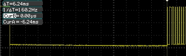
The sensor then pulls the signal line low for 80us followed by pulling up the signal line for a further 80us. At this point the sensor is ready to start to transmit the temperature and humidity data.
The data is transmitted by varying the length of time the signal pin is held high. Transmission of a single bit starts by pulling the signal line low. A 0 bit is indicated by the sensor pulling the signal line high for 26-28us. pulling the signal high for 70us indicates a 1.
The temperature and humidity data is transmitted in a 40-bit packet. The first 16 bits hold the humidity information, the next 16 bits hold the temperature information and the final 8 bits contains the checksum. The following shows the full data packet from the sensor:
Both the temperature and the humidity are represented as an integer. The actual value is obtained by converting the binary number to decimal and then dividing by 10. If the high bit of the temperature reading is 1 then the value represents a negative temperature.
The final 8 bits of the data packet contain the checksum. The checksum is the result of adding the four bytes of the temperature and humidity data.
Schematic
Aside from the components required to make a basic module, the board really only required two parts, a single pull-up resistor and the DHT22 Temperature and Humidity sensor itself.
The components to the left of the diagram should be familiar if you have read the previous posts on making a module. The only additional parts can be seen to the right of the schematic.
Breadboard and PCB Prototypes
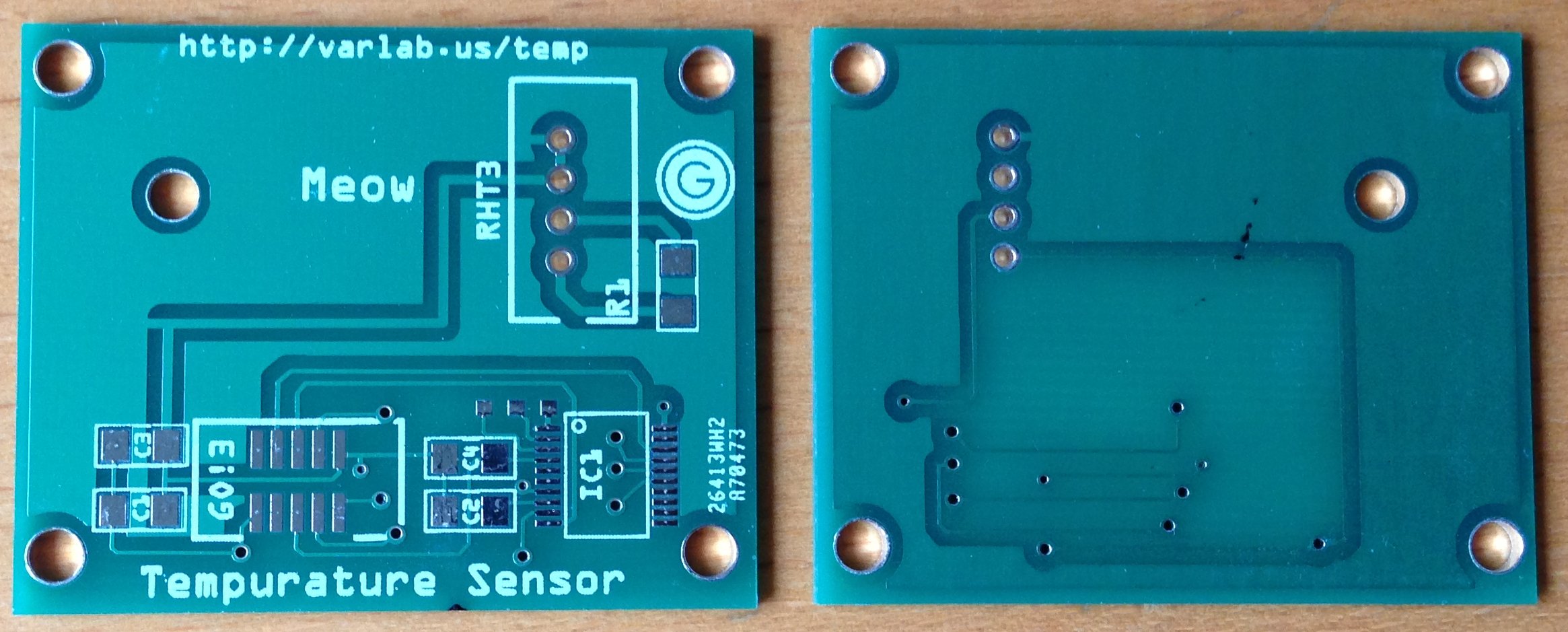
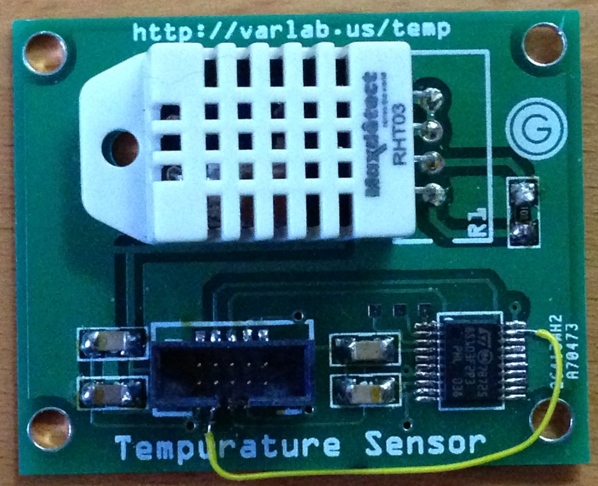
The original work for this module was completed on breadboard with an additional LM35 temperature sensor at the side of the DHT22. This second sensor was used as a reference to confirm the readings being generated by the DHT22. The simplicity of the design meant that moving to a PCB prototype was relatively simple and the iTeadStudio prototyping service made this affordable. A few weeks after ordering the prototype modules arrived:
One of the tests I do on any PCBs I have made is a connectivity test. I do this when the board is unpopulated and simply walk through the list of connections and verify that there are no problems. I also take the software I have written during prototyping on the breadboard and check that the pins on the STM8S are connected to the correct points on the PCB. It was during this test that I found that a connection had been missed off of the original schematic, namely the connection from the GO! connector and the GPIO pin which is used to signal that data is ready for the GO! to consume. A quick fix once the board had been populated.
Notice the yellow wire – this goes to show the value of prototyping even for the smallest and seemingly simplest of projects.
Software
The one wire protocol means that the microcontroller will be both a master and a slave device as will the DHT22. We also have to allow for the fact that we also have the leave a 2 second gap between readings. The ideal way to implement this is to use a finite state machine. The cycle of events is as follows:
Send the start signal and wait for 1-10ms
Enter read mode and collect data
Pause for at least 2 seconds
The state machine relies upon the timers to change the state based upon the minimum values for the time periods set by the sensor.
For the start signal, the signal line is set low and the timer started.
When the timer interrupt is triggered, the timer is turned off and reset. The signal pin is then switched from being an output pin to input with interrupts enabled. The timer is then restarted with a time period slightly larger than that required to ready all 40 bits of data from the sensor.
In the final stage, the interrupts are turned off, the data is processed and the system put to sleep (from a reading point of view) for more than 2 seconds.
In read mode, the system merely waits for interrupts to be generated by the sensor changing the state of the signal line. When an interrupt occurs, the time stamp (from the currently running timer) is read and recorded. The duration of the signal can then be calculated later (in stage three, pause mode) and the bit stream reconstructed from the timings.
Functionality
From a high level, the temperature and humidity module should provide the ability to read the current temperature and humidity (given the restrictions on the sensors delay of 2 seconds between readings). In addition, it would be desirable to allow the system to generate alarms for readings which are out of range.
As with all Netduino GO! modules, this functionality is split between the module and the module driver running on the Netduino GO!. The code on the module takes care of all the communication with the sensor. It takes this information and then responds to requests from the module driver on the Netdunio GO!.
STM8S Module
The software on the STM8S started life as the basic STM8S module software which has been used in previous posts.
The first modification needed is to add the state machine. The STM8S periodically reads the values from the sensor and store them for later retrieval by the Netduino GO! The regular nature of this update means that there is always a “current” reading available to the Netduiino GO! So the first thing we need is to setup a timer:
//--------------------------------------------------------------------------------
//
//  Setup Timer 2 to pause for 3.2 seconds following power up.
//
void SetupTimer2()
{
    TIM2_PSCR = 0x0a;       //  Prescaler = 1024
    TIM2_ARRH = 0xc3;       //  High byte of 50,000.
    TIM2_ARRL = 0x50;       //  Low byte of 50,000.
    TIM2_IER_UIE = 1;       //  Enable the update interrupts.
    TIM2_CR1_CEN = 1;
}
This initialisation code means that a reading is not available immediately. To go with this we will also need a variable to store the current mode along with some definitions:
//
//  Define the various modes for the state machine.
//
#define MODE_PAUSE                  0
#define MODE_SENDING_START_SIGNAL   1
#define MODE_READING_DATA           2
//
//  Current sensing mode.
//
int _mode = MODE_PAUSE;
Now for the critical part of the operation, we need to change to the correct state when the timer is triggered:
//--------------------------------------------------------------------------------
//
//  Timer 2 Overflow handler.
//
//  Note:   Normally we want the ISR to operate as quickly as possible but in
//          this case "as quickly as possible" just needs to be quick enough
//          for this sensor.  This means we have milliseconds for this ISR.
//
#pragma vector = TIM2_OVR_UIF_vector
__interrupt void TIM2_UPD_OVF_IRQHandler(void)
{
    TIM2_CR1_CEN = 0;
    switch (_mode)
    {
        case MODE_PAUSE:
            //
            //  Any pause has now completed, we need to start the
            //  read process.
            //
            PIN_DHT22_DATA = 0;
            TIM2_ARRH = 0xc3;       //  High byte of 50,000.
            TIM2_ARRL = 0x50;       //  Low byte of 50,000.
            TIM2_PSCR = 1;          //  Prescalar = 2 => count = 100,000 = 6.25mS
            TIM2_EGR_UG = 1;        //  Force counter update.
            _mode = MODE_SENDING_START_SIGNAL;
            break;
        case MODE_SENDING_START_SIGNAL:
            //
            //  At this point the start signal period has elapsed and we
            //  want to start to read data from the sensor.
            //
            PIN_DHT22_DATA = 1;
            PIN_DHT22_DIRECTION = 0;//  DHT22 pin is input.
            PIN_DHT22_MODE = 0;     //  DHT22 pin is floating input.
            EXTI_CR1_PDIS = 1;      //  Interrupt on rising edge.
            //
            //  We will get another interrupt after 5ms.  This should be
            //  enough time for the sensor to have generated the data and
            //  for us to process it.
            //
            TIM2_ARRH = 0x13;       //  High byte of 5,000.
            TIM2_ARRL = 0x88;       //  Low byte of 5,000.
            TIM2_PSCR = 4;          //  Prescalar = 4 => count = 5,000 (5 mS)
            TIM2_EGR_UG = 1;        //  Force counter update.
            _currentTiming = 0;
            _mode = MODE_READING_DATA;
            break;
        case MODE_READING_DATA:
            //
            //  At this point we should have read all of the data.  We
            //  now need to calculate the values and wait for 2 seconds
            //  before reading the next value.
            //
            PIN_DHT22_DATA = 1;     //  Set the output high after the data has been read.
            PIN_DHT22_DIRECTION = 1;//  DHT22 data pin is output.
            //
            //  We cannot read the sensor again for at least 2 seconds (32,800 with a prescalar
            //  of 11 should result in a ~4 seconds delay).
            //
            TIM2_ARRH = 0x80;
            TIM2_ARRL = 0x20;
            TIM2_PSCR = 0x0b;
            TIM2_EGR_UG = 1;        //  Force counter update.
            if (_currentTiming == 42)
            {
                DecodeData();
                if (_alarmsEnabled != 0)
                {
                    CheckAlarms();
                }
            }
            else
            {
                OutputStatusCode(SC_TOO_LITTLE_DATA);
            }
            _mode = MODE_PAUSE;
            break;
    }
    TIM2_CR1_CEN = 1;               //  Re-enable Timer 2.
    TIM2_SR1_UIF = 0;               //  Reset the interrupt otherwise it will fire again straight away.
}
Much of the code in the Interrupt Service Routine (ISR) above is concerned with recording the current state and resetting the timer ready to move into the next state. A key point to notice here is the change of use for the GPIO pin connected to the sensor.
When the ISR is entered and we are in pause mode (case MODE_PAUSE), we reset the timer and drop the signal line connected to the DHT22 (PIN_DHT22_DATA = 0). We then enter the next mode, MODE_SENDING_START_SIGNAL.
The next time the ISR is entered we should have just completed the time needed to keep the signal line low and for the sensor to be ready to send the data on the signal line. So we pull the signal line high and then change the direction of the GPIO line and the line becomes an input line which generates and interrupt. We then record the fact that we have changed to the next mode (MODE_READING_DATA), reset the timers and start to wait again.
In the final state, we should have received a full data packet from the sensor so we decode and process the data and then enter the pause mode once more. At this point the whole cycle repeats.
The state machine is now complete and we now need to start to look at recording the data. A little early experimentation showed that the sensor would generate 42 pulses. It was decided that the best way to record the pulses was to simply record the time at which they occurred. These timings could later be used to workout the pulse duration and hence if we had a 0 or 1. As we only needed the pulse duration then the actual time of the pulse was not needed, simply a reliable way of recording the duration. Timer 2 came to our aid. This timer was already running as it was required to control the state machine. We could simply record the value in this timer whenever an interrupt occurred. So starting with some definitions to support the storage of the data:
//
//  How many readings will we take?
//
#define MAX_READINGS                50
//
//  Somewhere to put the data.
//
int _sensorTimings[MAX_READINGS];
//
//  Which reading are we expecting next?
//
int _currentTiming = 0;
int _reading;
Next we need to capture the value in the timer when an interrupt occurred:
//--------------------------------------------------------------------------------
//
//  Process the interrupt generated by the DHT22.
//
#pragma vector = 8
__interrupt void EXTI_PORTD_IRQHandler(void)
{
    unsigned char high = TIM2_CNTRH;
    unsigned char low = TIM2_CNTRL;
    if (_currentTiming < MAX_READINGS)
    {
        _reading = (high << 8);
        _reading += low;
        _sensorTimings[_currentTiming++] = _reading;
    }
}
Now we have captured the data we need to decode the timings to obtain the temperature, humidity and the checksum. This method is called from the Timer 2 ISR above.
//--------------------------------------------------------------------------------
//
//  Decode the temperature and humidity data.
//
void DecodeData()
{
    unsigned short multiplier;
    //
    //  Extract the humidity.
    //
    unsigned short humidity = 0;
    multiplier = 32768;
    for (int index = 2; index < 18; index++)
    {
        if ((_sensorTimings[index] - _sensorTimings[index - 1]) > LOGIC_BOUNDARY)
        {
            humidity += multiplier;
        }
        multiplier >>= 1;
    }
    //
    //  Extract the temperature.
    //
    unsigned short temperature = 0;
    multiplier = 32768;
    for (int index = 18; index < 34; index++)
    {
        if ((_sensorTimings[index] - _sensorTimings[index - 1]) > LOGIC_BOUNDARY)
        {
            temperature += multiplier;
        }
        multiplier >>= 1;
    }
    //
    //  Extract the checksum.
    //
    unsigned short checksum = 0;
    multiplier = 128;
    for (int index = 34; index < 42; index++)
    {
        if ((_sensorTimings[index] - _sensorTimings[index - 1]) > LOGIC_BOUNDARY)
        {
            checksum += multiplier;
        }
        multiplier >>= 1;
    }
    //
    //  If the checksum is OK then overwrite the data.
    //
    unsigned short calcChecksum = 0;
    calcChecksum += humidity & 0xff;
    calcChecksum += ((humidity >> 8) & 0xff);
    calcChecksum += temperature & 0xff;
    calcChecksum += ((temperature >> 8) & 0xff);
    if ((calcChecksum & 0xff) == checksum)
    {
        _lastTemperature = temperature;
        _lastHumidity = humidity;
        _lastChecksum = checksum;
        OutputStatusCode(SC_OK);
        OutputDebugData(humidity, temperature, checksum);
    }
    else
    {
        OutputStatusCode(SC_CHECKSUM_ERROR);
    }
}
The LOGIC_BOUNDARY definition is simply the number of clock pulses which separates the 0 and the 1. A little empirical research gave this value as 100 clock pulses. This is not exactly as defined in the data sheet but it does give a reasonable working value.
As with all GoBus 1.0 modules, the definition of the data within the data packets (with the exception of the first byte) is left to the implementation. For this module the packets will be formatted as follows:
0x80 – Mandatory first byte
ACK or NACK
Type of data in the packet (for an ACK packet)
Data (for ACK)
The type of data in the packet allows the system to respond to requests for information and also raise alarms.
Responding to the requests for readings is simply a case of copying the last set of readings from the global variable and putting them into the packet. The module then raises an interrupt (via NotifyGOBoard()) to indicate to the Netduino GO! that there is some data ready for processing:
//--------------------------------------------------------------------------------
//
//  Copy the sensor readings into the _txBuffer.
//
void CopySensorReadingsToTxBuffer()
{
    _txBuffer[3] = ((_lastHumidity >> 8) & 0xff);
    _txBuffer[4] = (_lastHumidity & 0xff);
    _txBuffer[5] = ((_lastTemperature >> 8) & 0xff);
    _txBuffer[6] = (_lastTemperature & 0xff);
    _txBuffer[7] = _lastChecksum;
}

//--------------------------------------------------------------------------------
//
//  Notify the GO! main board that there is some data ready for collection.
//
void GetReadings()
{
    _txBuffer[0] = 0x80;
    _txBuffer[1] = DHT22_ACK;
    _txBuffer[2] = DHT22_GET_READINGS;
    CopySensorReadingsToTxBuffer();
    NotifyGOBoard();
}
One desirable feature mentioned earlier was the ability to set alarms and have the module signal to the Netduino GO! that an alarm has been raised. The alarm system allows the user to set an alarm for the following events:
Low temperature
High temperature
Low humidity
High humidity
Setting an alarm is a simple operation as it only requires that the module records the alarms which have been set and the values associated with the alarm:
//--------------------------------------------------------------------------------
//
//  Set the alarm thresholds for the temperature and humidity.
//
//  Note that the alarm uses "special" out of range values to indicate that a
//  specified limit is not required.
//
void SetAlarms()
{
    //
    //  Start by turning everything off.
    //
    _alarmsEnabled = 0;
    _lowerTemperatureAlarm = SENSOR_MIN_TEMPERATURE;
    _upperTemperatureAlarm = SENSOR_MAX_TEMPERATURE;
    _lowerHumidityAlarm = SENSOR_MIN_HUMIDITY;
    _upperHumidityAlarm = SENSOR_MAX_HUMIDITY;
    //
    //  Now work out what we are looking at.
    //
    if (_rxBuffer[2] & ALARM_LOW_TEMPERATURE)
    {
       _lowerTemperatureAlarm = (_rxBuffer[3] * 256) + _rxBuffer[4];
       if (_lowerTemperatureAlarm < SENSOR_MIN_TEMPERATURE)
       {
           _alarmsEnabled = 0;
           RaiseNAK();
           return;
       }
       _alarmsEnabled |= ALARM_LOW_TEMPERATURE;
    }
    if (_rxBuffer[2] & ALARM_HIGH_TEMPERATURE)
    {
        _upperTemperatureAlarm = (_rxBuffer[5] * 256) + _rxBuffer[6];
       if (_upperTemperatureAlarm > SENSOR_MAX_TEMPERATURE)
       {
           _alarmsEnabled = 0;
           RaiseNAK();
           return;
       }
        _alarmsEnabled |= ALARM_HIGH_TEMPERATURE;
    }
    if (_rxBuffer[2] & ALARM_LOW_HUMIDITY)
    {
       _lowerHumidityAlarm = (_rxBuffer[7] * 256) + _rxBuffer[8];
       if (_lowerHumidityAlarm < SENSOR_MIN_HUMIDITY)
       {
           _alarmsEnabled = 0;
           RaiseNAK();
           return;
       }
       _alarmsEnabled |= ALARM_LOW_HUMIDITY;
    }
    if (_rxBuffer[2] & ALARM_HIGH_HUMIDITY)
    {
        _upperHumidityAlarm = (_rxBuffer[9] * 256) + _rxBuffer[10];
       if (_upperHumidityAlarm > SENSOR_MAX_HUMIDITY)
       {
           _alarmsEnabled = 0;
           RaiseNAK();
           return;
       }
        _alarmsEnabled |= ALARM_HIGH_HUMIDITY;
    }
    //
    //  Tell the Go board which alarms have been enabled (as an acknowledgement).
    //
    _txBuffer[0] = 0x80;
    _txBuffer[1] = DHT22_ACK;
    _txBuffer[2] = DHT22_SET_ALARMS;
    _txBuffer[3] = _alarmsEnabled;
    NotifyGOBoard();
}
The actual process of raising the alarm is performed in the Timer 2 ISR when we have decoded the data. Remember this code:
DecodeData();
if (_alarmsEnabled != 0)
{
    CheckAlarms();
}
When checking the alarms the application will compare the values for all of the alarms and then raise a single interrupt back to the Netduino GO! if one or more alarms need to be raised. The data packet sent back to the Netduino GO! also contains the current sensor readings. This means that the Netduino GO! does not have to request the sensor data to find out which alarm has been raised.
//--------------------------------------------------------------------------------
//
//  Check to see if the temperature/humidity is outside of any ranges and raise
//  an alarm if needed.
//
void CheckAlarms()
{
    unsigned char alarm = 0;
    if ((_alarmsEnabled & ALARM_LOW_TEMPERATURE) && (_lastTemperature < _lowerTemperatureAlarm))
    {
        alarm |= ALARM_LOW_TEMPERATURE;
    }
    if ((_alarmsEnabled & ALARM_HIGH_TEMPERATURE) && (_lastTemperature > _upperTemperatureAlarm))
    {
        alarm |= ALARM_HIGH_TEMPERATURE;
    }
    if ((_alarmsEnabled & ALARM_LOW_HUMIDITY) && (_lastHumidity < _lowerHumidityAlarm))
    {
        alarm |= ALARM_LOW_HUMIDITY;
    }
    if ((_alarmsEnabled & ALARM_HIGH_HUMIDITY) && (_lastHumidity > _upperHumidityAlarm))
    {
        alarm |= ALARM_HIGH_HUMIDITY;
    }
    if (alarm != 0)
    {
        _txBuffer[0] = 0x80;
        _txBuffer[1] = DHT22_ACK;
        _txBuffer[2] = DHT22_ALARM;
        CopySensorReadingsToTxBuffer();
        _txBuffer[8] = alarm;
        NotifyGOBoard();
    }
}
At this point the majority of the STM8S code is complete.
Netduino GO!
As with the STM8S code, the Netduino GO! driver is based upon the code developed previously and used as the basis for the Output Expander module. Much of this should be familiar and so we will only be considering the methods and supporting structures which implement specific features in this module. The class diagram for our module driver looks like this:
As you can see the module driver is not overly complex as it provides a few methods and supports a single interrupt.
The STM8S module returns temperature data on two occasions, the first is the explicit request by the Netduino GO! for the current readings, the second is when an alarm is raised. It therefore makes sense to abstract this code into a method:
/// <summary>
/// Extract the temperature and humidity data from the data which has been
/// generated by the STM8S.
/// </summary>
/// <param name="temperature">Temperature extracted from the buffer.</param>
/// <param name="humidity">Humidity extracted from the buffer.</param>
private void ExtractSensorReadings(out float temperature, out float humidity)
{
    //
    //  Verify the checksum before extracting the data.
    //
    int sum = 0;
    for (int index = 4; index < 8; index++)
    {
        sum += _readFrameBuffer[index];
    }
    if ((sum & 0xff) == _readFrameBuffer[8])
    {
        //
        //  Checksum good so extract the temperature and humidity data.
        //
        humidity = ((float) ((_readFrameBuffer[4] * 256) + _readFrameBuffer[5])) / 10;
        int sign = 1;
        byte highByte = _readFrameBuffer[6];
        if ((highByte & 0x80) == 0x80)
        {
            sign = -1;
            highByte &= (byte) 0x7f;
        }
        temperature = sign * ((float) ((highByte * 256) + _readFrameBuffer[7])) / 10;
    }
    else
    {
        throw new Exception("ExtractSensorData: Checksum error, discarding data.");
    }
}
The code which gets the current readings is relatively trivial:
/// <summary>
/// This method calls the AddOne method on the GO! module and then waits for the
/// module to indicate that there is a response ready.  The response is then read
/// from the module and the resulting value is returned to the caller.
/// </summary>
public void GetReadings()
{
    _writeFrameBuffer[0] = GO_BUS10_COMMAND_RESPONSE;
    _writeFrameBuffer[1] = (int) Action.GetReadings;
    WriteDataToModule();
    if (!WaitForResponse())
    {
        throw new Exception("GetReadings: Cannot communicate with the DHT22 module");
    }
}
Setting an alarm is also trivial, although the method is longer, with much of the work involving extracting the bytes of data and storing them in the transmit buffer:
/// <summary>
/// Set the alarms for the low/high temperature/humidity alarms.
/// </summary>
/// <remarks>
/// To turn an alarm off set the value to float.MinValue.
///
/// The alarms are triggered when the temperature/humidity goes below the low threshold
/// or above the high threshold.
/// </remarks>
/// <param name="lowTemperature">Low temperature alarm value.</param>
/// <param name="highTemperature">High temperature alarm value.</param>
/// <param name="lowHumidity">Low humidity alarm value.</param>
/// <param name="highHumidity">High humidity alarm value.</param>
public void SetAlarms(float lowTemperature, float highTemperature, float lowHumidity, float highHumidity)
{
    Alarms alarms = 0;

    if (lowTemperature != float.MinValue)
    {
        if ((lowTemperature < MIN_TEMPERATURE) || (lowTemperature > MAX_TEMPERATURE))
        {
            throw new ArgumentOutOfRangeException("SetAlarms: lowTemperature out of range.");
        }
        short lt = (short) (lowTemperature * 10);
        _writeFrameBuffer[3] = (byte) ((lt & 0xff00) >> 8);
        _writeFrameBuffer[4] = (byte) (lt & 0xff);
        alarms |= Alarms.LowTemperature;
    }
    if (highTemperature != float.MinValue)
    {
        if ((highTemperature > MAX_TEMPERATURE) || (highTemperature < MIN_TEMPERATURE))
        {
            throw new ArgumentOutOfRangeException("SetAlarms: highTemperature out of range.");
        }
        short ht = (short) (highTemperature * 10);
        _writeFrameBuffer[5] = (byte) ((ht & 0xff00) >> 8);
        _writeFrameBuffer[6] = (byte) (ht & 0xff);
        alarms |= Alarms.HighTemperature;
    }
    if (lowHumidity != float.MinValue)
    {
        if ((lowHumidity < MIN_HUMIDITY) || (lowHumidity > MAX_HUMIDITY))
        {
            throw new ArgumentOutOfRangeException("SetAlarms: lowHumidity out of range");
        }
        short lh = (short) (lowHumidity * 10);
        _writeFrameBuffer[7] = (byte) ((lh & 0xff00) >> 8);
        _writeFrameBuffer[8] = (byte) (lh & 0xff);
        alarms |= Alarms.LowHumidity;
    }
    if (highHumidity != float.MinValue)
    {
        if ((highHumidity < MIN_HUMIDITY) || (highHumidity > MAX_HUMIDITY))
        {
            throw new ArgumentOutOfRangeException("SetAlarms: highHumidity out of range");
        }
        short hh = (short) (highHumidity * 10);
        _writeFrameBuffer[9] = (byte) ((hh & 0xff00) >> 8);
        _writeFrameBuffer[10] = (byte) (hh & 0xff);
        alarms |= Alarms.HighHumidity;
    }
    _writeFrameBuffer[0] = GO_BUS10_COMMAND_RESPONSE;
    _writeFrameBuffer[1] = (int) Action.SetAlarms;
    _writeFrameBuffer[2] = (byte) alarms;
    WriteDataToModule();
    if (!WaitForResponse())
    {
        throw new Exception("SetAlarms: Cannot communicate with the DHT22 module");
    }
}
The really interesting work involves the receipt of data from the module. This is triggered by the interrupt being raised on the GPIO pin of the Netduino GO! connector.
/// <summary>
/// Handle the IRQ events generated by the GO! module.
/// </summary>
/// <remarks>
/// The module raises an interrupt when a command has been processed or when there
/// is data ready for the module.  The first task for this method is to retrieve
/// the buffer from the module and then work out what action should be taken.  The
/// module will have placed any relevant data into the write buffer prior to raising
/// the interrupt.
/// </remarks>
private void _irqPort_OnInterrupt(uint data1, uint data2, DateTime time)
{
    _writeFrameBuffer[0] = GO_BUS10_COMMAND_RESPONSE;
    _writeFrameBuffer[1] = (int) Action.GetBuffer;
    WriteDataToModule();
    if ((_readFrameBuffer[1] == GO_BUS10_COMMAND_RESPONSE) && (_readFrameBuffer[2] == DHT22_ACK) && ReadBufferCRCCheckOK())
    {
        float t, h;

        switch ((Action) _readFrameBuffer[3])
        {
            case Action.GetReadings:
                ExtractSensorReadings(out t, out h);
                Temperature = t;
                Humidity = h;
                _irqPortInterruptEvent.Set();
                break;
            case Action.SetAlarms:
                _irqPortInterruptEvent.Set();
                break;
            case Action.Alarm:
                if ((SensorAlarm != null) && (AlarmInterruptsEnabled == AlarmState.InterruptsEnabled))
                {
                    ExtractSensorReadings(out t, out h);
                    SensorAlarm(this, new AlarmEventArgs(t, h, (Alarms) _readFrameBuffer[9]));
                }
                break;
            default:
                throw new ArgumentException("Interrupt: Unknown action " + _readFrameBuffer[3].ToString());
                break;
        }
    }
}
This event allows the main program to set an alarm and then leave the module to work out when it needs to communicate with the Netduino GO!. This is achieved by the application setting the delegate SensorAlarm
Testing
At this point we have the hardware and software complete. All that is needed now is to put the two together:
A quick test application (I promise, this will be last piece of the code in this article):
The image above shows the DHT22 module connected to the Netduino GO!. A Komodex Labs Seven Segment Display is used to display the temperature and humidity.
And here is a video showing the module working. The system shows the temperature for a short while (16.8C) followed by the humidity (46.7%).
We were lucky last year as we had a particularly cold winter (lucky for testing). This allowed the module to be test outdoors in a reasonably cold environment. The sensor and the Netduino GO! performed as expected down to -10C when compared to an off the shelf digital thermometer and humidity unit. I would have waited for the temperature to drop further by my desire to prove the module has limits and I discovered that standing around outside with a coffee waiting for the module to read lower and lower temperatures had an interest threshold of about 10 minutes.
Conclusion
This module shows the power of combining microcontrollers to provide a combined system. The Netduino GO! would have found it difficult to have achieved the work completed by the STM8S. Similarly, the Netduino GO! provides the application developer with the simplicity and power of NETMF, something the STM8S could not achieve.
This module has yet to move from prototype into production. Maybe it will someday, just not today.
Sometimes you have to do something just because you can. Today was no exception. Take one Raspberry Pi board (Linux) and give it a dose of .NET loving…
I can hear people screaming NO! but it’s too late, I’ve done it.
To be honest, I’m not the first person to use .NET on the Raspberry Pi. In fact I used this installation guide to install Mono on the Raspberry Pi.
So what interested me? Simply put, hardware interfacing. Could the .NET hardware classes (i.e. SerialPort) be used on the Raspberry Pi? There was only one way to find out.
Raspberry Pi Setup
The first thing to do was to set up the Raspberry Pi using the instructions in the blog mentioned above. This was not difficult although it was time consuming as it took a while to compile.
When this is complete a simple program should demonstrate if the serial ports are available to us. The following code should show this:
namespace ConsoleApplication1
{
	class Program
	{
		public static void Main(string[] args)
		{
			SerialPort sp = new SerialPort("/dev/ttyAMA0", 115200, Parity.None, 8, StopBits.One);
			sp.Open();
			for (int index = 0; index < 10; index++)
			{
				string result = string.Format("{0} Testing", index);
				sp.Write(result);
			}
			sp.Close();
		}
	}
}
As you can see, this code is not too complex. It merely opens a serial port and then starts to output data to the port. The only tricky part of the job was to locate the name to be used for the serial port. It’s been too long since I used Unix in anger.
Testing the Application
Testing is not too complex as the test application is simply outputting a text message. We can see the output by hooking up PuTTY to a serial port on a computer.
The hardware is also simple to hook up. The FTDI cable I have allows me to connect a 3.3V TTL serial device to my PC over USB. This USB device then appears as a standard serial device on the PC. Three connections are required:
Raspberry Pi
FTDI Cable
Ground
Ground
Rx
Tx
Tx
Rx
Strictly speaking, we do not have to connect the Tx on the FTDI cable to the Rx on the Raspberry Pi as we will not be transmitting anything from the PC to the Raspberry Pi in this example.
Once the hardware is connected you will need to fire up PuTTY and connect it to the serial port on your PC. Ensure that the settings used match those in the application code above.
Assuming that you now have Mono installed and the application typed in ready to go, type the following commands into a shell on the Raspberry Pi:
mcs serial.cs
mono serial.exe
The first command invokes the Mono C# compiler. The second tells mono to execute the application which has been compiled.
If all has gone well then you will see something like this in the PuTTY window running on the PC:
Serial Output in Putty
Conclusion
I was rather interested to see that the C# skills acquired on the PC could also be used on the Raspberry Pi. The only thing missing on the Pi was a good development environment.
Making the OutputExpander module has been an interesting journey. The original drawings started in August 2012 and then sat on the hard drive for about eight months. Much of the time following the original drawings were spent working out how the STM8S worked. You can find out more in The Way of the Register series (something I will pick up again soon, to my mind there are a few missing topics).
For those who do not know, I’m a software engineer and electronics is a hobby. The prospect of designing a board and using SMD components would have been unthinkable to me two years ago. Today I sit here with my first prototype PCB connected to a commercial board and the output looks reasonably professional – well I’ll let you decide.
Completed Board
Not looking too bad if I say so myself.
So let’s look at what I have learned and also how long the project took.
Lessons Learned
With all projects we should look back and learn from the experience, both good and bad. So here are a few things I have learned over the past few months.
Designing the Board
The original design started life in August 2012. I probably should have taken the plunge and developed the board a little quicker than I did although in truth, I did not get the major requirement of the board, namely GoBus 1.0 really sorted out until late November 2012.
Prototyping
This was probably the simplest bit of the project. I have all of the standard components in my toolbox already and I also have the tools required. This was really a case of getting the system working. The hardest part was getting to grips with the STM8S, a story I have documented in The Way of The Register series of posts.
Schematic
During this part of the design phase I tried several different packages. All of them had strengths and weaknesses. I finally settled on DesignSpark. For me this package had three major strengths:
It’s free
You can use it for commercial projects
It feels like a Windows application
In fairness it does have a few weaknesses. The most obvious for me was the lack of the ability to add images of any kind to the design. Come on, at version 5 you should have this one!
Nets – I discovered these when producing the final draft of the schematic. These allowed the separation of the nets into logical groups/functions/areas. It made the schematic a lot cleaner.
Schematic to Manufacture
For me this was the where I learned the most. The first thing I learned was that auto-routers are dreadful. They are slow and produce some interesting board layouts. This board is a simple board and yet the auto-router still took a long time to make a half-hearted attempt at routing the board. In the end I did this manually. This was not too much of a problem as the board was simple.
Next, you have to learn to think in three dimensions. You have two layers so use them.
The Netduino modules produced by Secret Labs have nice rounded corners – these are a devil to produce in DesignSpark. I think that the module I produced has one corner which is slightly different from the others.
The cost of prototyping is a lot lower than I thought. Ten boards including shipping costs about £18 and only took 10 days.
I now know what 0403 means. The ‘0’ stands for Ohhh my goodness that’s small. Seriously, the four digits should be split into two and thy give the dimensions of the component. So for a metric component an 0403 part is 0.4 x 0.3 mm – that’s small.
The STM8S part selected has a 0.65mm pitch for the pins. I originally found this a little worrying. Don’t be afraid – they are not that bad.
Get a USB microscope when soldering SMD components. This tools is cheap and allows the examination of joints for shorts. The quality will never be great, mine only runs at 640×480, but a 400x zoom means you can be sure that you have no problems.
Add test points. There came a point when I was making the board and I needed to see the data going through to the 74HC595’s. I did not have a suitable connection and so I had to solder a piece of wire to the board:
Improvised Test Point
A good test point would have made this easier.
How Long Did it Take
The original drawing started in August 2012 and the final board was put together and tested only yesterday. So in elapsed time that’s about nine months. In real working time this broke down as follows:
Activity
Duration (Hours)
Building Prototype circuit
2
Prototype software
3
Schematic
6
PCB layout
20
Assembly and testing
5
Enhanced software
4
Total
40
Something to bear in mind is that no production evaluation or component selection has been conducted as part of this project. It was supposed to be the final item on the list. I am still not sure if this should be taken through to manufacture – time will tell.
Another item to be considered is to achieve the Netduino GO! logo approval. At the time of writing this required the approval of the board by Secret Labs – this activity has not been completed.
Conclusion
Well, that was a hectic few weeks.
Did I enjoy it – YES!
Would I recommend that you try it – YES!
As for me, I’ll be taking a few days off of hardware development and blogging. Love doing it but it can take it’s toll.
I suppose you may be interested in some downloads…
If you use any of the code or techniques discussed in this series of posts then please let me know as I’m interested in what other people are doing with this work.
This series of posts follows the steps required in order to make your own Netduino GO! module. To do this we are using a simple idea, an Output Expander (yes, it seems to have a name now) for the Netduino GO!. Using only a hand full of simple components, the Output Expander will add 32 digital outputs to the Netduino Go!.
The Story So Far…
The module has so far completed the following steps:
Concept and prototype on breadboard
Basic drivers
PCB design and layout
Generation of PCB manufacturing files
The first batch of 10 boards were ordered on 20th April 2013 using iTeads prototyping service. I am expecting the manufacturing process to take about one week with a further two weeks for shipping as I used the cheap, slow courier service.
In the meantime we still have the breadboard prototype to work with. This may only have two shift registers attached to it but by carefully parametrising the code we should be able to develop a driver which only needs to be recompiled when the final hardware becomes available.
Features
The driver for this module should be relatively simple as we are merely setting outputs from the shift registers to be either on or off. We shall start with the following list of desired features:
Default initialisation to set up for one board
Set the bytes for the digital outputs
Array like access for the bits
Configurable latching mode (automatic or manual)
Clear the output
Turn outputs from the registers on or off
The only remaining task is to decide where the features are to be implemented. We have two options:
On the Netduino GO! in C#
On the STM8S in C
Some of the code is better left on the Netduino GO! with the base features (setting all of the register values etc) being implemented on the STM8S.
Initialisation
Initialisation should allow for the use of cascaded boards. If you look back at the schematic you will notice a connector called CascadeConn. This connector allows the addition of a simpler board as an expansion module. This board only need to supply additional shift registers leaving the first, main board supplying the logic to communicate with the Netduino GO!. The concept is that if you want 64 outputs then you would have a single Output Expander module with a single, cheaper daughter board.
In order to support the addition of the daughter board the initialisation will need to support the specification of the number of shift registers in the cascade.
In supporting the cascading of these boards we will also need to provide some sensible default values. The basic case is a single board which contains four shift registers.
We should also consider a maximum value for the number of shift registers. In this case I am going to set this to 12 for two reasons:
Power considerations – all of the power for the shift registers is being provided by the Netduino GO!
Data packet size – the data packets used in the GoBus are fixed size. Keeping the number of shift registers to a value where only one data packet is required simplifies the communication between the Netduino GO! and the module as a single packet can be used for all messages.
In order to facilitate this we will need code on both the Netduino GO! and the module.
Module Code
The code on the module should allow for the number of shift registers to be set up (assuming a default value of four registers) and then clear the registers. The default code should be called when the module is re-initialised.
//--------------------------------------------------------------------------------
//
//  GO! function 3 - Set up the module.
//
void SetUp()
{
    U8 n = _rxBuffer[2];
    if ((n < 0) && (n < MAX_REGISTERS))
    {
        _numberOfShiftRegisters = n;
        free(_registers);
        _registers = (U8 *) malloc(n);
        ClearRegisters();
        OutputData();
        NotifyGOBoard();
    }
}
Netduino GO! Code
The initialisation code on the Netduino GO! will assume that the startup code on the module will initialise itself to four shift registers. This will reduce the communications overhead between the Netduino GO! and the module. The following when added to the Initialise method should set up the module driver on the Netduino GO! for a variable number of shift registers in the sequence:
//
//  Next, set up the space to store the data.
//
_shiftRegisterData = new byte[numberOfShiftRegisters];
for (int index = 0; index < numberOfShiftRegisters; index++)
{
    _shiftRegisterData[index] = 0;
}
LatchMode = LatchingMode.Automatic;
if (numberOfShiftRegisters != 4)
{
    _writeFrameBuffer[0] = GO_BUS10_COMMAND_RESPONSE;
    _writeFrameBuffer[1] = CMD_SETUP;
    _writeFrameBuffer[2] = (byte) (numberOfShiftRegisters & 0xff);
    WriteDataToModule("Initialise: cannot setup the OutputExpander module");
}
Set Outputs
Setting the outputs is simply a case of sending a number of bytes, one for each shift register to the module.
/// <summary>
/// Set the shift registers using the values in the byte array.
/// "/summary>
/// "param name="registers">Bytes containing the shift register values.</param>
public void Set(byte[] registers)
{
    if (registers.Length != _shiftRegisterData.Length)
    {
        throw new ArgumentException("registers: length mismatch");
    }
    for (int index = 0; index < registers.Length; index++)
    {
        _shiftRegisterData[index] = registers[index];
    }
    Latch();
}
The module code needs a slight adjustment to transfer the correct number of incoming bytes to the register store:
//--------------------------------------------------------------------------------
//
//  GO! function 2 - Output the specified bytes to the shift registers.
//  Tx buffer.
//
void SetShiftRegisters()
{
    for (int index = 0; index < _numberOfShiftRegisters; index++)
    {
        _registers[index] = _rxBuffer[2 + index];
    }
    OutputData();
    NotifyGOBoard();
}
Array of Bits
From a software point of view, a shift register is nothing more than an array of boolean values. Internally it makes sense for the driver to allow this abstraction and use the indexing operator to set a single bit at a time. The code for this operator looks something like this:
/// <summary>
/// Overload the index operator to allow the user to get/set a particular
/// bit in the shift register.
/// </summary>
/// <param name="bit">Bit number to get/set.</param>
/// <returns>Value in the specified bit.</returns>
public bool this[int bit]
{
    get
    {
        if ((bit >= 0) && (bit < (_shiftRegisterData.Length * 8)))
        {
            int register = bit >> 3;
            byte mask = (byte) (bit & 0x07);
            return ((_shiftRegisterData[register] & mask) == 1);
        }
        throw new IndexOutOfRangeException("OutputExpander: Bit index out of range.");
    }
    set
    {
        if ((bit >= 0) && (bit < (_shiftRegisterData.Length * 8)))
        {
            int register = bit >> 3;
            byte mask = (byte) ((1 << (bit & 0x07)) & 0xff);
            if (value)
            {
                _shiftRegisterData[register] |= mask;
            }
            else
            {
                mask = (byte) ~mask;
                _shiftRegisterData[register] &= mask;
            }
            if (LatchMode == LatchingMode.Automatic)
            {
                Latch();
            }
        }
        else
        {
            throw new IndexOutOfRangeException("OutputExpander: Bit index out of range.");
        }
    }
}
Adding the above code allows the programmer to use constructs such as:
OutputExpander outputs = new OutputExpander();
outputs[2] = true;
instead of the more obscure:
OutputExpander outputs = new OutputExpander();
byte[] data = new byte[4];
data[0] = 0x04;
SetOutputs(data);
Not only is the former example more elegant but it is also more concise.
Clear All Registers
This method will simply clear the shift registers and set the outputs to 0;
/// <summary>
/// This method calls the ClearRegister method on the GO! module and then waits for the
/// module to indicate that it has received and executed the command.
/// </summary>
public void Clear()
{
    _writeFrameBuffer[0] = GO_BUS10_COMMAND_RESPONSE;
    _writeFrameBuffer[1] = CMD_CLEAR_REGISTERS;
    for (int index = 0; index < _shiftRegisterData.Length; index++)
    {
        _shiftRegisterData[index] = 0;
    }
    WriteDataToModule("Clear cannot communicate with the Output Expander module");
}
This method could have been rewritten to set the values to 0 and then send the values to the module. However, the prototype already had an implementation of a clear command and so this was left in as is.
Latch Mode
The introduction of the array indexing operators does introduce on complication, namely that we cannot set all of the outputs to a specified value at the same time without delaying the latching of the registers. Consider the following case:
In this case we would set bit 2 of the lower shift register followed by bit 3 of the same shift register. Because of the speed of .NETMF there would be a slight delay between the two outputs of the shift register being set high. In order to allow for this we introduce the ability to delay the latching of the data from the internal shift register into the output register.
/// <summary>
/// Determine when the data should be sent to the module.
/// </summary>
public enum LatchingMode
{
    /// <summary>
    /// Automtically send the data to the module as soon as there are any changes.
    /// </summary>
    Automatic,
    /// <summary>
    /// Manually latch the data.
    /// </summary>
    Manual
}

/// <summary>
/// Backing variable for the LatchMode property.
/// </summary>
private LatchingMode _latchMode;

/// <summary>
/// Determine how the data will be send to the module.  The default is to
/// automatically send data as soon as there are any changes.
/// </summary>
public LatchingMode LatchMode
{
    get { return (_latchMode); }
    set { _latchMode = value; }
}
The initialisation of the class would also need to be modified in order to set the mode to automatic:
LatchMode = LatchingMode.Automatic;
The most lightweight method of using the LatchMode is to simply not send the data to the shift registers until the mode is either reset or until the controlling program explicitly latches the data. The Set method will therefore need some adjustment to take into account the two modes:
/// <summary>
/// Set the shift registers using the values in the byte array.
/// </summary>
/// <param name="registers">Bytes containing the shift register values.</param>
public void Set(byte[] registers)
{
    if (registers.Length != _shiftRegisterData.Length)
    {
        throw new ArgumentException("registers: length mismatch");
    }
    for (int index = 0; index < registers.Length; index++)
    {
        _shiftRegisterData[index] = registers[index];
    }
    if (LatchMode == LatchingMode.Automatic)
    {
        Latch();
    }
}
Latch Operation
The introduction of the LatchMode means that we also need to allow for the data to be latched into the shift registers.
/// <summary>
/// Call the Set command on the module to set the outputs of the shift registers.
/// </summary>
private void Set()
{
    _writeFrameBuffer[0] = GO_BUS10_COMMAND_RESPONSE;
    _writeFrameBuffer[1] = CMD_SET_REGISTERS;
    for (int index = 0; index < _shiftRegisterData.Length; index++)
    {
        _writeFrameBuffer[2 + index] = _shiftRegisterData[index];
    }
    WriteDataToModule("Latch cannot communicate with the Output Expander module");
}
The above method simply sends the data to the module.
Testing
We can perform some simple testing of the software while the prototype boards are being made by using the breadboard test environment build in the first post. This board only has two shift registers but it should be possible to test the majority of functionality using this board.
In the previous posts we have cycled through the bits one at a time either from 0 to 15 or down from 15 to 0. In this example we will perform some counting and use the LEDs to display the number in binary. Our test code becomes:
output = new OutputExpander(2);
short cycleCount = 0;
byte[] registers = new byte[2];
output.LatchMode = OutputExpander.LatchingMode.Manual;
while (true)
{
    Debug.Print("Cycle: " + ++cycleCount);
    short mask = 1;
    output.Clear();
    for (int index = 0; index <= 15; index++)
    {
        if ((cycleCount & mask) != 0)
        {
            output[index] = true;
        }
        mask <<= 1;
    }
    output.Latch();
    Thread.Sleep(200);
}
Deploying this application should result in the Netduino GO! counting up from 0 and the binary representation of cycleCount being output on the shift registers. The following video shows this in action:
Conclusion
The above minor modifications to the STM8S module code and the Netduino GO! driver has added the following functionality:
Default initialisation to set up for one board
Set the bytes for the digital outputs
Array like access for the bits
Configurable latching mode (automatic or manual)
Clear the output
Turn outputs from the registers on or off
The code has been carefully written so that we should only need to change two parameters when the final PCBs arrive in order to change the drivers from two shift registers to four shift registers.
A quick test has shown that the main functionality appears to be working on the breadboard prototype as demonstrated by the above video. The prototype PCBs have completed manufacture and are currently with the Hong Kong postal service (as of 27th April 2013). Delivery should take another 7-10 days so there is plenty of time to complete the test suite.
This website uses cookies to improve your experience and to gather page view statistics. This site does not collect user information. Accept & CloseRead More
Privacy & Cookies Policy
Privacy Overview
This website uses cookies to improve your experience while you navigate through the website. Out of these, the cookies that are categorized as necessary are stored on your browser as they are essential for the working of basic functionalities of the website. We also use third-party cookies that help us analyze and understand how you use this website. These cookies will be stored in your browser only with your consent. You also have the option to opt-out of these cookies. But opting out of some of these cookies may affect your browsing experience.
Necessary cookies are absolutely essential for the website to function properly. This category only includes cookies that ensures basic functionalities and security features of the website. These cookies do not store any personal information.
Any cookies that may not be particularly necessary for the website to function and is used specifically to collect user personal data via analytics, ads, other embedded contents are termed as non-necessary cookies. It is mandatory to procure user consent prior to running these cookies on your website.