RSS

Archive for the ‘Netduino’ Category

Netduino Cube Information

Sunday, September 11th, 2011

Whilst the blog may have been a little quiet recently I have never the less been busy writing about the cube. There is a Wiki article on the Netduino web site showing how the cube was constructed.

I have also released the source code to the project on Codeplex.

8 x 8 x 8 LED Cube – Powered by Netduino

Sunday, July 10th, 2011

I’m just about to start to write this up but I thought I’d share the cube working before I do. Here is a video showing a few animations:

Watch this space for more information over the coming days.

So What’s All This About a Matrix?

Tuesday, July 5th, 2011

In a previous post I mentioned that replacing a single LED in the centre of a matric would be murder and so it will be. The matrix I have in mind is an 8 x 8 x 8 LED cube controlled by a Netduino board. Now it should be obvious that there are not enough pins to connect 512 LEDs to the Netduino without some magic being involved. This is where the Persistence of Vision post comes into the picture. In theory, it should be possible to control an array using a group of shift registers and a multiplexer circuit. So for the next few weeks this is what I’ll be looking at.

Multi-Threading

The previous post on Persistence of Vision had a simple while loop which allowed 16 LEDs to be controlled from the main program loop. In the final program this will be too cumbersome and timing is almost certainly to become an issue. To overcome this we will need to have the display logic separated from the control logic. This will allow the display to be continuously updated whilst the main program loop is working out what should be displayed next. The following tests this concept by turning on on LED at a time in a bank of 8. If this project has a chance of working then the 8 LEDs should all appear to be switched on permanently.

Hardware

The hardware is relatively simple. We have one shift register connected to the Netduino. This is in turn connected to 8 LEDs through current limiting resistors. The schematic looks something like this:

Persistence of Vision Threaded Display Driver Test Circuit

Software

The software requires us to take the display logic from previous posts and add this to a new class. This class will need to have a method executing in it’s own thread in order to allow the main program and the display driver to run at the same time. So splitting the display code into it’s own class we get something like this:

class LEDCube
{
    /// <summary>
    /// SPI bus to use to send data to the shift registers.
    /// </summary>
    SPI spi = null;

    /// <summary>
    /// CSPI bus configuration
    /// </summary>
    SPI.Configuration config;

    /// <summary>
    /// Buffer holding the display data.
    /// </summary>
    private byte[] buffer;

    /// <summary>
    /// Constructor for the LEDCube class.
    /// </summary>
    public LEDCube()
    {
        config = new SPI.Configuration(SPI_mod: SPI.SPI_module.SPI1,
                                       ChipSelect_Port: Pins.GPIO_PIN_D9,
                                       ChipSelect_ActiveState: false,
                                       ChipSelect_SetupTime: 0,
                                       ChipSelect_HoldTime: 0,
                                       Clock_IdleState: true,
                                       Clock_Edge: true,
                                       Clock_RateKHz: 400);

        spi = new SPI(config);
        buffer = new byte[1];
        buffer[0] = 0;
    }

    /// <summary>
    /// Main loop which continuously updates the display from the buffer.
    /// </summary>
    public void DisplayBuffer()
    {
        while (true)
        {
            lock (buffer)
            {
                spi.Write(buffer);
            }
        }
    }

    /// <summary>
    /// Change the byte in the display buffer.
    /// </summary>
    /// <param name="b">Byte to put into the buffer.</param>
    public void UpdateBuffer(byte b)
    {
        lock (buffer)
        {
            buffer[0] = b;
        }
    }
}

Much of the code should be familiar, we have the SPI bus and config variables along with a constructor to make a new instance of the SPI bus. The new code is really the DisplayBuffer and the UpdateBuffer methods.

  • DisplayBuffer is the method which has replaced the part of the main program loop which outputs the data to the SPI bus. This method is run in it’s own thread.
  • UpdateBuffer simply copies new data from the caller into the display buffer.

Note that both of these methods use locking to ensure that the methods are thread safe.

The main program loop now looks something like this:

LEDCube cube = new LEDCube();
Thread display = new Thread(new ThreadStart(cube.DisplayBuffer));
display.Start();
while (true)
{
    byte value = 1;
    for (int index = 0; index < 8; index++)
    {
        cube.UpdateBuffer(value);
        value <<= 1;
    }
}

A new LEDCube is created and at first this is not running in it’s own thread. The next two lines create and start a new thread. The thread is executing the DisplayBuffer method. We then start the main program lopp which simply sets each bit in a byte and the updates the buffer in the cube using UpdateBuffer.

Next step, build the control logic for 512 LEDs.

Persistence Of Vision

Saturday, June 11th, 2011

By chance last week end I came across a post discussing persistence of vision. This set me wondering if I could demonstrate this using the Netduino. First a little background.

Background

Persistence of vision is the phenomena which allows you to watch a movie. The projector shows a single still image on the screen. This is then replaced 1/24th of a second later by a new image. The projector achieves this by covering the image with a shutter whilst the frame is moved into place. We do not see the blank screen, just the previous frame. A fuller description can be found on this Wikipedia page.

We will be using this effect to control 27 LEDs using only 11 control lines. These lines will be the outputs from two 74595 shift registers which in turn will be connected to a Netduino Plus.

The Problem

The 27 LEDs will be split into three banks of 9. The aim will be to write a small program which will turn on one or more of the of the 9 LEDs in each bank in turn. If we do this slowly we will see bank 1 turn on whilst banks 2 and 3 are off. Next we will see bank 1 turn off, bank 2 will turn on and bank 3 will remain off, and so on. In theory, if we do this fast enough, we will see all three banks on at the same time.

Hardware

This project uses the hardware and principles from two previous projects:

  1. Netduino Controlling an External LED (using a transistor as a switch)
  2. Counting Using 74595 Shift Registers

A picture is worth a thousand words so lets have a look at the schematic:

Persistence of Vision Schemaic

The two shift registers are connected to the Netduino using the SPI interface. The output from IC1 is fed to the serial input of IC2 creating 16 output lines (8 from each register). These lines will power the LEDs and select the bank to turn on.

The LEDs will be powered using bits 0 to 7 of IC1 and bit 0 of IC2.

The top three bits of IC2 will select which bank to turn on. This is done using a transistor as a switch.

The trick to controlling the banks and LEDs lies in the way the circuit is wired up. The anodes of LED1, LED10 and LED19 are connected together and then connected to QA of IC1. Similarly, the anodes of LED2, LED11 and LED20 are connected to QB of IC1. This continues until all 27 LEDs have been connected to the 9 control lines (QA-QH of IC1 and QA of IC2).

The next part of the trick is to connect the cathodes from the LEDs in bank 1 together. These are then connected to a current limiting resistor which is in turn connected to the collector of a 2N2222 NPN transistor. This is repeated with banks 2 and 3 being connected similarly to their own transistor.

The base of each transistor is connected through a resistor to one of the bank control outputs pins (QF, QG and QH) of IC2. The emitter is connected to ground.

Note that in theory it is possible to turn on all three banks at once by setting the appropriate bits in the shift register but the object of this exercise is to show how to make a still image using each bank in turn.

Software

The software uses SPI to send two bytes to the 74595 shift registers. The values sent will control which LEDs are turned on / off. The code looks like this:

SPI.Configuration config;
config = new SPI.Configuration(SPI_mod: SPI.SPI_module.SPI1, ChipSelect_Port: Pins.GPIO_PIN_D9, ChipSelect_ActiveState: false, ChipSelect_SetupTime: 0, ChipSelect_HoldTime: 0, Clock_IdleState: true, Clock_Edge: false, Clock_RateKHz: 400);
SPI spi = new SPI(config);
byte[] value = new byte[2];
value[1] = 0xff;
while (true)
{
    value[0] = 0x81;
    spi.Write(value);
    value[0] = 0x41;
    spi.Write(value);
    value[0] = 0x21;
    spi.Write(value);
}

If you run this code you will see a still image with all three banks looking as though they are permanently on. Set a breakpoint on the line value[0] = 0x81; and run the program again. Single stepping will show each bank being turned on in turn. The reason we see the still image is because the banks are turned on and off quickly.

Putting it all together and wiring it up on breadboard gives you this:

Persistence Of Vision On Breadboard

Persistence Of Vision On Breadboard

Counting Using 74HC595 Shift Registers

Thursday, June 2nd, 2011

Following the post earlier this week regarding the implementation of a ShiftRegister class which allows the Netduino to control a series of 74HC595 shift registers I had a look at what would be needed to make the system count and show the output in binary on a series of LEDs. What you see here is the result. The hardware is the same as the previous post, only the software has changed.

One of the main desires is to allow the programmer to use the natural language features of C# to work with this class. The modifications should therefore support operations such as assignment, logical and etc. The main program loop for a counter should look something like this:

ShiftRegister shiftRegister = new ShiftRegister(16, Pins.GPIO_PIN_D9);
for (ushort index = 0; index < 10000; index++)
{
    shiftRegister = index;
    Debug.Print("Count: " + index + ", " + shiftRegister.ToString());
    shiftRegister.LatchData();
    Thread.Sleep(100);
}

In order to support this we will need to overload the implicit assignment operator for an unsigned short being assigned to a ShiftRegister instance. This results in the following code:

/// <summary>
/// Overload the assignment operator.
/// </summary>
/// <param name="usi">Unsigned short integer to assign to the register.</param>
/// <returns>New ShiftRegister holding the unsigned short value.</returns>
public static implicit operator ShiftRegister(ushort usi)
{
    ShiftRegister result = new ShiftRegister(16);   // ushorts are 16 bits.

    ushort mask = 1;
    for (int index = 0; index < 16; index++)
    {
        result._bits[index] = (usi & mask) > 0;
        mask <<= 1;
    }
    return (result);
}

This generates some problems with the base shift register class from the last post. Most noteably the creation of the SPI instance. The run-time system will generate an error should the programmer try and create two objects wanting to access the SPI bus. Reading the above code you can see that the assignment overload requires a new ShiftRegister instance to be created. A few changes are therefore required in order to allow the system to share the same interface. In order to allow this, the base class moves the SPI object from a shared instance to a static object. This ensures that only one of these can exist at any time. The remaining modifications to the class support this change and add a ToString() method for debugging. The modified code and a sample test project can be found here and the following video shows the application in action.

Further Developments

The base functionality assumed that the class is the only class wanting to use the SPI bus. The number of chips and breakout boards using is large and so it is likely that the programmer will want to communicate with several slave devices using the same bus. This is allowed using the SPI protocol and for the moment this is left as an exercise for the reader.

74HC595 Shift Registers

Monday, May 30th, 2011

The 7400 family of chips have for many years provided a set chips which implement common logic functions. The 74HC595 is a member of this family and provides an eight bit serial-in, parallel-out shift register. This register also provides a pin which can be used to cascade these chips providing a longer sequence of bits if required. In this post we will look at this chip and implement a C# class which can be used to set / reset individual bits in a series of cascaded shift registers. This is very much a software engineers view on how to access a shift register.

74HC595

Those of you who are familiar with the principles and operations of a shift register can skip the next section and move on the the implementation.

Shift Register Overview

A shift register in its simplest form is a series of bits. Data is shifted into the register using serial communication on bit at a time. Each time a bit is pushed into the shift register it moves all those to the right of it one place to the right with the bit at the end being discarded. For example, consider the following four bit register:

b3b2b1b0
1000

Adding a new bit with the value 0 results in the following:

b3b2b1b0Discarded
01000

The 74HC595 has an additional pin which allows the output of the discarded bit. By feeding this discarded bit into another 75HC595 you can build up a chain of cascaded chips to make a larger shift register.

Hardware

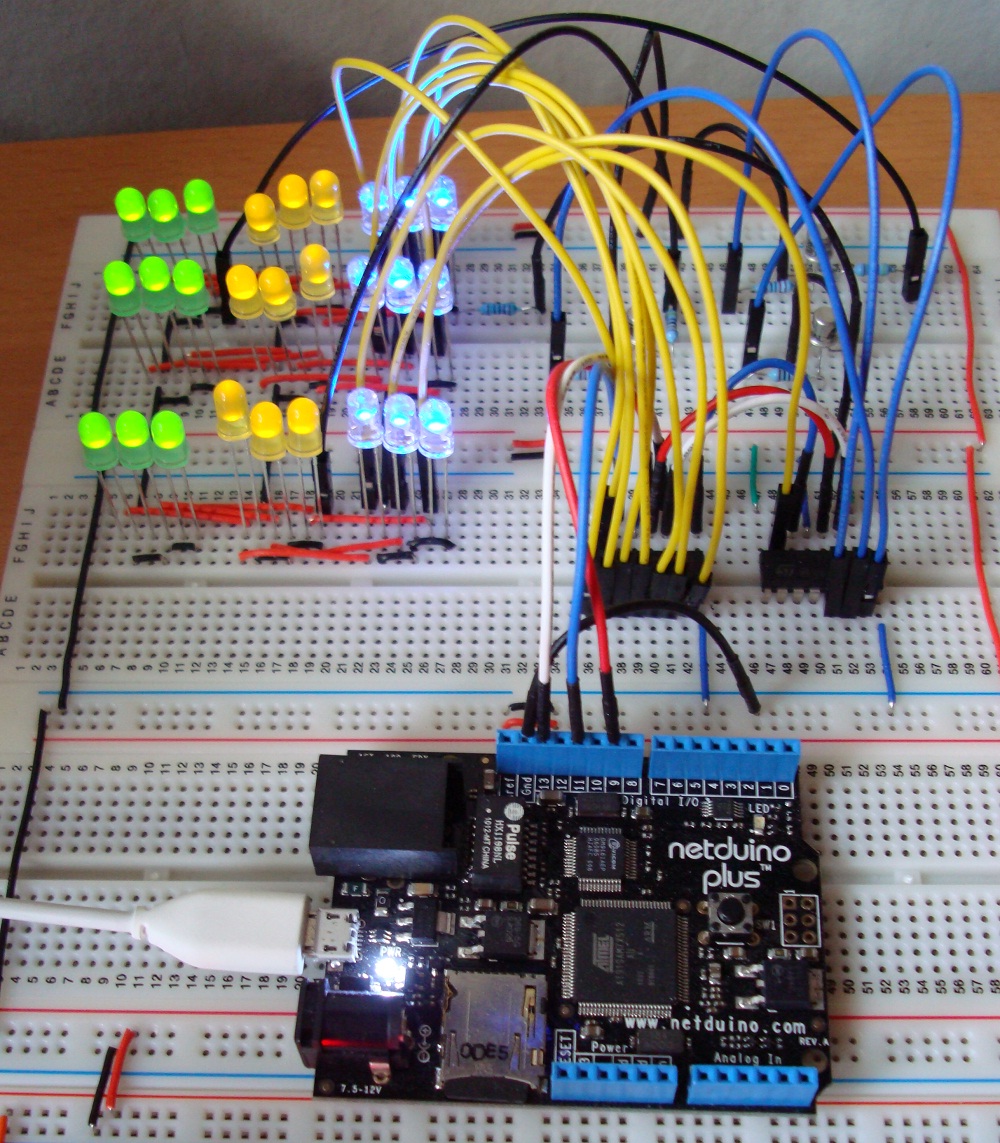
A simple LED driver is used to illustrate the hardware and software principles used. The hardware will use two 74HC595’s (although it is possible to use more) to drive a bank of LEDs (one per output for each chip). The bill of materials becomes:

ItemQuantityNotes
74HC5952
LEDs16One for each output pin on the 74HC595’s.
47 Ohm Resistor1
Netduino Plus1
WireLots of itYou really will need lot of it.

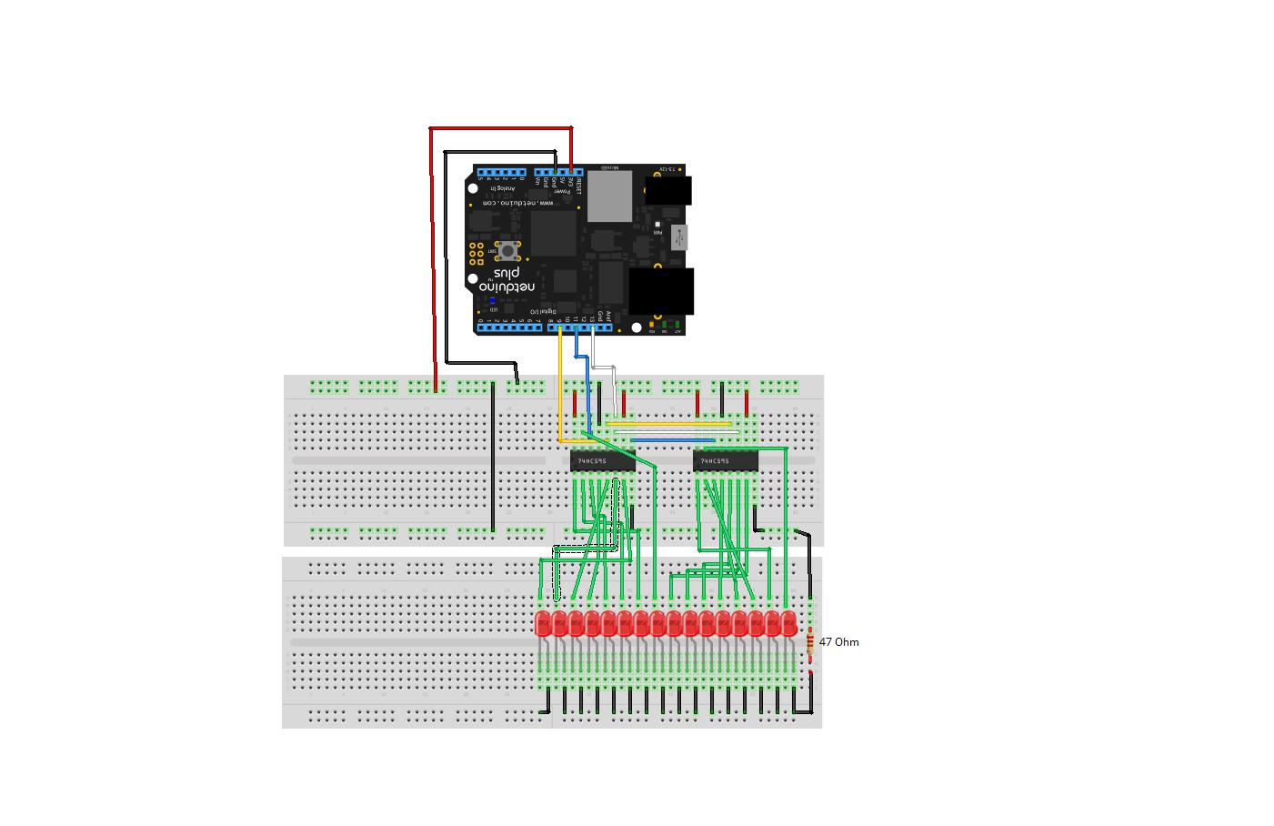
The LEDs are really there just to give an instant visual interpretation of the output from the shift registers and to prove the software is working. The way they are wired up and the resistor used to limit the current means that the more LEDs are powered, the dimmer they will be. The wiring looks something like this:

Shift Register Cascade

Shift Register Cascade

Looking at the diagram, the wiring seems confusing. The green wires show the wiring of the LEDs to the outputs of the shift registers. The outputs of the shift register should be wired to the LEDs from right to left in the order QA through QH. This is probably the most confusing part of the diagram due to the number of connections but these all follow the simple principle of wiring the output from the chip to the LED and then through to ground.

If we throw away the green connections then we have a few key connections:

  1. SI on the left most shift register (pin 14) should be connected to MOSI on the Netduino.
  2. SCK on the left most shift register (pin 11) should be connected to SPCK on the Netduino
  3. /G on the left shift register (pin 13) should be connected to the latch pin on the Netduino
  4. RCK on the left shift register (pin 12) should be connected to ground

When cascading the registers the following connections should be made for the registers to the right of the first register:

  1. Serial Out (pin 9) of the left chip to SI (pin 14) of the right chip
  2. SCK of both chips (pin 11) should be connected
  3. /G on both chips (pin 13) should be connected

The data is fed into the shift registers from the left with bit 0 appearing on the far right. The clock and the enable is fed into both chips at the same time. The serial data is fed into the chip on the far left and is cascaded on to the chip to it’s immediate right. Further chips can be added to the right and cascaded in the same manner. In this way, bit 0 will always be at the far right of the shift registers.

Software

The software used the SPI interface on the Netduino to communicate with the shift registers. An important note in the documentation is that the chip has a two stage process for transferring the data from the input to the output. Each bit is transferred into the shift register on the rising edge of the clock pulse. This is then transferred on to the output on the following rising edge. This is fine for all but the last bit as it will need a rising edge in order to be transferred to the output. Standard SPI has the idle clock set to low. As such this could lead to the final bit not being transferred to the output. In order to overcome this the SPI interface was set to the idle clock being high. The final transition from an active clock to an idle clock will then trigger the transfer of the final bit from the input to the output.

From a software engineers point of view a shift register is nothing more than an array of boolean values and this is the approach that was taken. The software holds an array of boolean values (multiples of 8 bits as the shift registers targeted are 8 bit registers). The software holds an array of values which the programmer can then choose to output to the registers.

The variable declarations become:

/// <summary>
/// Array containing the bits to be output to the shift register.
/// </summary>
private bool[] _bits;

/// <summary>
/// Number of chips required to implement this ShiftRegister.
/// </summary>
private int _numberOfChips;

/// <summary>
/// SPI interface used to communicate with the shift registers.
/// </summary>
private SPI _spi;
The variable holding the number of chips is used to help the runtime performance by not having to recalculate the number of chips on each transfer to the hardware.

The constructor for the class instantiates the array holding the number of bits in the shift register and the SPI interface:

public ShiftRegister(int bits, Cpu.Pin latchPin = Cpu.Pin.GPIO_Pin8, SPI.SPI_module spiModule = SPI.SPI_module.SPI1, uint speedKHz = 10)
{
    if ((bits > 0) && ((bits % 8 ) == 0))
    {
        _bits = new bool[bits];
        _numberOfChips = bits / 8;
        for (int index = 0; index < bits; index++)
        {
            _bits[index] = false;
        }

        SPI.Configuration config;

        config = new SPI.Configuration(SPI_mod: spiModule, ChipSelect_Port: latchPin, ChipSelect_ActiveState: false, ChipSelect_SetupTime: 0, ChipSelect_HoldTime: 0,  Clock_IdleState: true, Clock_Edge: false, Clock_RateKHz: speedKHz);

        _spi = new SPI(config);
    }
    else
    {
        throw new ArgumentOutOfRangeException("ShiftRegister: Size must be greater than zero and a multiple of 8 bits");
    }
}

A little bit operator overloading on the indexer allows the programmer to address the individual bit in the shift register:

/// <summary>
/// Overload the index operator to allow the user to get/set a particular 
/// bit in the shift register.
/// </summary>
/// <param name="bit">Bit number to get/set.</param>
/// <returns>Value in the specified bit.</returns>
public bool this[int bit]
{
    get
    {
        if ((bit >= 0) && (bit < _bits.Length))
        {
            return (_bits[bit]);
        }
        throw new IndexOutOfRangeException("ShiftRegister: Bit index out of range.");
    }
    set
    {
        if ((bit >= 0) && (bit < _bits.Length))
        {
            _bits[bit] = value;
        }
        else
        {
            throw new IndexOutOfRangeException("ShiftRegister: Bit index out of range.");
        }
    }
}

The final piece of the jigsaw is to allow the programmer to send the data to the shift register:

/// <summary>
/// Send the data to the SPI interface.
/// </summary>
public void LatchData()
{
    byte[] data = new byte[_numberOfChips];

    for (int chip = 0; chip < _numberOfChips; chip++)
    {
        data[chip] = 0;
        byte bitValue = 1;
        int offset = chip * 8;
        for (int bit = 0; bit < 8; bit++)
        {
            if (_bits[offset + bit])
            {
                data[chip] |= bitValue;
            }
            bitValue <<= 1;
        }
    }
    _spi.Write(data);
}

This method is really the work horse as it converts the bits into an array of bytes which are transferred to the shift registers.

Testing it Out

Testing should be easy, lets walk through all of the bits for a 16 bit register made by having two shift register connected together:

public static void Main()
{
    ShiftRegister shiftRegister = new ShiftRegister(16, Pins.GPIO_PIN_D9);
    while (true)
    {
        for (int index = 0; index < 16; index++)
        {
            shiftRegister[index] = true;
            shiftRegister.LatchData();
            Thread.Sleep(100);
            shiftRegister[index] = false;
        }
    }
}

This example uses two registers (16 bits) and uses pin D9 as the enable pin for the register. The code sets, displays and then resets each bit starting at bit 0 through to bit 15.

The full code for the shift register class can be found here (ShiftRegister.zip).

Windows Application Communicating with Netduino Over USB

Saturday, May 28th, 2011

Whilst the Netduino Plus has the advantage of being able to communicate with a PC by networking, the Netduino and the Netduino Mini do not have this capability built in. The simplest way of communicating with these two devices is probably by a serial connection. Both of these devices differ in the capabilities, one has two TTL COM ports whilst the other (the Netduino Mini) has a RS232 COM port and a TTL COM port.

This article discusses the connection using the TTL COM port to a PC using a USB connection. This is applicable to the Netduino, the Netduino Plus and the Netduino Mini.

USB Connection

Before we can start to write any software we need to make the physical connection. There are a few options available, a breakout board which converts the USB connection into a serial connection or a cable which has the conversion hardware built in. I went for the later option as this seemed simpler. The cable I purchased was the FTDI 5V VCC 3.3V IO cable. Plugging this cable into the PC installed new drivers (on Windows 7) and created a new COM port for me.

Connecting the cable was simple, The ground on the cable connected to the ground on the Netduino. The Tx and Rx connections needed to be crossed. So Rx on the cable went to the Netduino digital pin 1 and Tx on the cable connected to Netduino digital pin 0.

Software

This solution requires two projects, a Windows Forms application and a Netduino application.

Windows Form Application

This application will simply send commands in the form of lines of text down the serial port to the Netduino. Each command will terminate with a r character. This application is simple and mimics sending a command to turn an LED on or off.The application looks like this:

Windows Serial Interface

Windows Serial Interface

Clicking the LED On button sends the string LED=1 down the serial line to the listening device. Similarly, clicking on LED Off button sends the command LED=0 to the device.

The code to achieve this is trivial and there are only three parts, the first is to create the connection (see MainForm_Load) and the second and third parts send the command to the device (see btnLEDOn_Click and btnLEDOff_Click).

/// <summary>
/// Initialise the application.
/// </summary>
private void MainForm_Load(object sender, EventArgs e)
{
	com6 = new SerialPort("COM6", 9600, Parity.None, 8, StopBits.One);
	com6.Open();
}

/// <summary>
/// Send a command to the device listening on the com port.
/// </summary>
private void btnLEDOn_Click(object sender, EventArgs e)
{
	com6.Write("LED=1\r");
}

/// <summary>
/// Send a command to turn the LED off.
/// </summary>
private void btnLEDOff_Click(object sender, EventArgs e)
{
	com6.Write("LED=0\r");
}

Netduino Application

The Netduino application is a little more complex as it has to listen to the serial port and assemble a buffer containing the commands being received. The achieve this I abstracted the serial port processing into a separate class. This class took care of listening to the serial port and building up a beffer. The class then provided a way of reading a line of text from the buffer and presenting this to the caller as a single entity. The main code for this is contained in the class CommPort and can be found in the SerialComms.cs file in the attached project.

The main program loop becomes a simple affair and looks like this:

public static void Main()
{
    CommPort port = new CommPort(SerialPorts.COM1, BaudRate.Baudrate9600, Parity.None, 8, StopBits.One);
    while (true)
    {
        string text = port.ReadLine();
        if (text.Length != 0)
        {
            Debug.Print("Command: " + text);
        }
        Thread.Sleep(1000);
    }
}

To run the code I compiled the Windows Form application and then navigated (using Windows explorer) to the directory containing the executable. Double clicking on this started the application and opened the COM port. Next I deployed the Netduino application to the Netduino and with the debugger attched I clicked on the LED On button in the Windows application. A short time later the text Command: LED=1 appeared in the debug window.

The code for this project can be found here (WinFormSerialExample.zip).

Netduino and Bluetooth (RN-42)

Sunday, April 24th, 2011

After many a hour playing (and swearing) I think I have now managed to get the Netduino talking to a Bluetooth module in command mode. There were many teething problems along the way but I think the source code which is attached along with the notes should allow the reconfiguration/control of the Bluetooth module from the Netduino.

Objective

There were two objectives for this project, namely

  1. Allow a PC to send data to the Netduino over a Bluetooth device
  2. Provide a mechanism for the Netduino to reconfigure a Bluetooth device

This is a mainly software project as the connections are straightforward.

The Hardware

The Bluetooth module chosen was a Roving Networks RN-42. This device can be found on a breakout board on several hardware sites (Proto-Pic or Sparkfun) and provides a simple COM connection to the Netduino.

Wiring up the module was simple, only six connections to worry about 🙂

  1. CTS and RTS – connect these together.
  2. Vcc – connect to 3.3V
  3. GND – connect to ground (make sure this is connected to the ground on the Netduino as well)
  4. TX – connect to RX on the Netduino (I was using COM1 so connect to RX on the Netduino – Digital pin 1)
  5. RX – connect to TX on the Netduino (I was using COM1 so connect to TX on the Netduino – Digital pin 0)

There were a few teething problems along the way. The major issue was that at the time I was not able to get access to the correct documentation for the module. A little persistence and I finally had it.

So the first task was to get the module talking to my PC. Powering on the module and then getting my PC to search for Bluetooth device was simple. The PC found the device and paired without much fuss. I opened PuTTY and set the COM port parameters and I was talking to the module.

This is where it started to get interesting (i.e. frustrating) as I had missed a crucial part of the documentation. In order to enter command mode you must enter the command string within 60 seconds of the module being powered up. Once I had this figured it was a doddle. PuTTY allowed me to enter commands and displayed the responses.

So at this point I knew I had a working Bluetooth module and it could connect to the the PC in both data and command mode.

Software

The next problem was to bring the module under the control of the Netduino. This required the a few design decisions. The module can return both single and multi-line responses to commands.

The simplest problem was the single line response. The system simply looped until a line of data was returned.

For the multi-line response it was necessary to allow the system some processing time. The approach taken was to allow the user to specify a wait time. This would allow the Bluetooth module to fill the buffer with response to the command. This puts the Netduino to sleep far a while. Again, this was considered acceptable as the system would be configuring the Bluetooth module – i.e. a startup overhead rather than a run-time overhead.

Usage

The library is pretty simply to use with the constructor taking the parameters needed to create a new instance of the class and connect it to the Bluetooth module and the few remaining public methods allowing the user to talk to the module.

Constructor

The public constructor takes five parameters which essentially allow the class to configure the serial port used to communicate with the module.

public RovingNetworks(string port, BaudRate baudRate, Parity parity, int dataBits, StopBits stopBits)

EnterCommandMode

This method switches the module into command mode. It must be called within 60 seconds (if using default configuration) of the module being turned on.

ExitCommandMode

This method returns the module to data mode.

This methods has two variants. The first is used for simple commands and returns a single string which is the one line response from the module. The second is for more verbose commands where more than one line is returned from the module.

For the majority of commands only one line of test is returned and so the simple one line method can be used. This will loop until a response has been received by the system. This response is then returned to the user.

public string SendCommand(string command)
{
    string result;

    ClearBuffer();
    _bluetoothModule.Write(Encoding.UTF8.GetBytes(command), 0, command.Length);
    result = ReadLine();
    while (result == "")
    {
        result = ReadLine();
    }
    return (result);
}

The second method assumes a multi-line response from the command. In order to collect these responses together the system pauses a while. It is important that this pause is long enough for the module to process the command and generate the response but not too long as this will block the thread for the specified timeout period.

public ArrayList SendCommand(string command, int timeout)
{
    ArrayList result;
    string line;

    ClearBuffer();
    result = new ArrayList();
    _bluetoothModule.Write(Encoding.UTF8.GetBytes(command), 0, command.Length);
    Thread.Sleep(timeout);
    line = ReadLine();
    while (line != "")
    {
        result.Add(line);
        line = ReadLine();
    }
    return (result);
}

Example

The following small program shows the execution of a single command which returns some configuration information for the module.

RovingNetworks rn42;

rn42 = new RovingNetworks(Serial.COM1, BaudRate.Baudrate115200, Parity.None, 8, StopBits.One);
if (rn42.EnterCommandMode())
{
    Debug.Print("Success");
    ArrayList result = rn42.SendCommand("Drn", 500);
    foreach (string str in result)
    {
        Debug.Print(str);
    }
    Thread.Sleep(Timeout.Infinite);
}
else
{
    Debug.Print("Oh dear...");
}

The code is available RN 42 Bluetooth Source Code There’s not a lot of it and it’s reasonably well commented so we’ll call it a day.

Edit (25th April 2011): Implemented IDispose and updated the source code.

4 Digit, 7 Segment Display – Part 2 – Ouput an Unsigned Short

Tuesday, March 15th, 2011

Update 18 March 2011: This is where this series of posts finishes for the minute as I appear to have fried the MAX7219 (or something else is wrong with the setup) as I can send commands to it but the output does not make any sense. I’ll have to return to this series when I have a new chip.

This is the second in a series of posts discussing the MAX7219 LED driver chip being used to drive a four digit, seven segment LED display. The series is made up of the following posts:

  1. Part 1 – Output a Byte
    Output a series of bytes from the Netduino Plus using the SPI protocol
  2. Part 2 – Output an Unsigned Short (This Post)
    Similar to the first post but this time we will write a series of short integers using SPI. This will also start to implement the code which will write the data to the MAX7219 chip.
  3. Part 3 – Displaying Numbers
    Using the MAX7219 class to display a number on the display
  4. Part 4 – Displaying Sensor Data
    Hooking up a sensor to the Netduino and displaying the reading from the sensor.

Objective

The objective of this post is to start to flesh out the code (which will be presented in the final post) to start to send commands in the form of 16 bit unsigned shorts to the MAX7219.

All of the hardware remains as before and only the software changes. As before, the logic analyser is used to verify the results.

Software

The software required a minor update to convert the output to an array of ushorts and put the register in the msb and the data in the lsb.

Results

The main program does little more that send two commands to the logic analyser, namely a command to enter normal operation followed by a command to restrict the number of digits to four.

The results can be seen here:

This image shows the command to restrict the display to four digits being sent over the SPI bus.

The next step is to complete the wiring and to start to send display data to the MAX7219.

4 Digit, 7 Segment Display – Part 1 – Ouput a Byte

Tuesday, March 15th, 2011

Update 18 March 2011: This is where this series of posts finishes for the minute as I appear to have fried the MAX7219 (or something else is wrong with the setup) as I can send commands to it but the output does not make any sense. I’ll have to return to this series when I have a new chip 🙁

This series of posts will discuss using the MAX7219 LED driver chip to drive a four digit, seven segment LED display. The series is made up of the following posts:

  1. Part 1 – Output a Byte (This Post)
    Output a series of bytes from the Netduino Plus using the SPI protocol
  2. Part 2 – Output an Unsigned Short
    Similar to the first post but this time we will write a series of short integers using SPI. This will also start to implement the class which will write the data to the MAX7219 chip.
  3. Part 3 – Displaying Numbers
    Using the MAX7219 class to display a number on the display
  4. Part 4 – Displaying Sensor Data
    Hooking up a sensor to the Netduino and displaying the reading from the sensor.

Background Reading

The following posts provide some background information as these are similar projects:

Objective

The objective of these post is to connect the Netduino Plus to the breadboard and get a 5V logic signal representing a series of bytes. In order to do this it is necessary to convert the output from the Netduino Plus from 3.3V to 5V. I propose to experiment and use a 7408 quad 2 input AND gate to convert the 3.3V signal up to 5V. So for this post we will need the following components:

  1. Netduino Plus
  2. 1 x 74HCT08N quad 2 input AND gate
  3. Breadboard with 5V power supplied to the power rails
  4. Wire to connect the components

Theory

Part of this exercise is to see if we can convert a 3.3V signal into a 5V signal. This is necessary as the MAX7219 uses 5V inputs. The quad input AND gate was chosen to do this for no other reason than I had a few spare in the component box. The data sheet for this chip states that the minimum voltage for a high input is 3.15V when the chip is supplied with 4.5V. A quick experiment shows that a 3.3V input signal to this chip does indeed result in a high output.

So by connecting one of the inputs to the AND gate to 5V and the second to the signal source, then the output from the gate should reflect the input but translated from 3.3V to 5V.

One point to note is that the chip will take a little while for the signal on the inputs to be reflected on the output pins. This application will be running at a low frequency (10KHz) and so the chip should be able to keep up.

Software

The software is a simple starter program which cycles through the bytes from 0 to 255 and output’s these bytes on the SPI bus. The Saleae logic analyser is used to verify that the data is being output correctly. A small test program should demonstrate that the data is being transmitted on the bus correctly:

using System;
using System.Net;
using System.Net.Sockets;
using System.Threading;
using Microsoft.SPOT;
using Microsoft.SPOT.Hardware;
using SecretLabs.NETMF.Hardware;
using SecretLabs.NETMF.Hardware.NetduinoPlus;

namespace NetduinoPlusTestApplication
{
    public class Program
    {
        public static void Main()
        {
            SPI.Configuration config;
            SPI spi;
            byte[] b;

            config = new SPI.Configuration(Pins.GPIO_PIN_D10, false, 0, 0, false, false, 10, SPI.SPI_module.SPI1);
            spi = new SPI(config);
            b = new byte[1];

            while (true)
            {
                for (byte v = 0; v <= 255; v++)
                {
                    b[0] = v;
                    spi.Write(b);
                    Thread.Sleep(20);
                }
            }
        }
    }
}

Hardware

The following table shows how the Netduino Plus is connected to the 74HCT08N

74HCT08NConnection
2, 5, 10, 13, 14+5V
7Ground
12Netduino Plus digital pin 10 (used for CS)
1Netduino Plus digital pin 11 (MOSI)
4Netduino Plus digital pin 13 (Clock)

The ground on the Netduino Plus should also be connected to the ground on the breadboard.

Results

After completing the wiring the logic analyser was hooked up and the following trace appeared:

Scrolling through the trace show each of the ASCII characters being interpreted correctly.

So the next step it to start to build the class which will talk to the MAX7219.