RSS

Archive for the ‘Electronics’ Category

Persistence Of Vision

Saturday, June 11th, 2011

By chance last week end I came across a post discussing persistence of vision. This set me wondering if I could demonstrate this using the Netduino. First a little background.

Background

Persistence of vision is the phenomena which allows you to watch a movie. The projector shows a single still image on the screen. This is then replaced 1/24th of a second later by a new image. The projector achieves this by covering the image with a shutter whilst the frame is moved into place. We do not see the blank screen, just the previous frame. A fuller description can be found on this Wikipedia page.

We will be using this effect to control 27 LEDs using only 11 control lines. These lines will be the outputs from two 74595 shift registers which in turn will be connected to a Netduino Plus.

The Problem

The 27 LEDs will be split into three banks of 9. The aim will be to write a small program which will turn on one or more of the of the 9 LEDs in each bank in turn. If we do this slowly we will see bank 1 turn on whilst banks 2 and 3 are off. Next we will see bank 1 turn off, bank 2 will turn on and bank 3 will remain off, and so on. In theory, if we do this fast enough, we will see all three banks on at the same time.

Hardware

This project uses the hardware and principles from two previous projects:

  1. Netduino Controlling an External LED (using a transistor as a switch)
  2. Counting Using 74595 Shift Registers

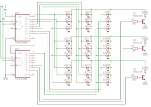
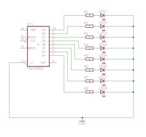
A picture is worth a thousand words so lets have a look at the schematic:

Persistence of Vision Schemaic

The two shift registers are connected to the Netduino using the SPI interface. The output from IC1 is fed to the serial input of IC2 creating 16 output lines (8 from each register). These lines will power the LEDs and select the bank to turn on.

The LEDs will be powered using bits 0 to 7 of IC1 and bit 0 of IC2.

The top three bits of IC2 will select which bank to turn on. This is done using a transistor as a switch.

The trick to controlling the banks and LEDs lies in the way the circuit is wired up. The anodes of LED1, LED10 and LED19 are connected together and then connected to QA of IC1. Similarly, the anodes of LED2, LED11 and LED20 are connected to QB of IC1. This continues until all 27 LEDs have been connected to the 9 control lines (QA-QH of IC1 and QA of IC2).

The next part of the trick is to connect the cathodes from the LEDs in bank 1 together. These are then connected to a current limiting resistor which is in turn connected to the collector of a 2N2222 NPN transistor. This is repeated with banks 2 and 3 being connected similarly to their own transistor.

The base of each transistor is connected through a resistor to one of the bank control outputs pins (QF, QG and QH) of IC2. The emitter is connected to ground.

Note that in theory it is possible to turn on all three banks at once by setting the appropriate bits in the shift register but the object of this exercise is to show how to make a still image using each bank in turn.

Software

The software uses SPI to send two bytes to the 74595 shift registers. The values sent will control which LEDs are turned on / off. The code looks like this:

SPI.Configuration config;
config = new SPI.Configuration(SPI_mod: SPI.SPI_module.SPI1, ChipSelect_Port: Pins.GPIO_PIN_D9, ChipSelect_ActiveState: false, ChipSelect_SetupTime: 0, ChipSelect_HoldTime: 0, Clock_IdleState: true, Clock_Edge: false, Clock_RateKHz: 400);
SPI spi = new SPI(config);
byte[] value = new byte[2];
value[1] = 0xff;
while (true)
{
    value[0] = 0x81;
    spi.Write(value);
    value[0] = 0x41;
    spi.Write(value);
    value[0] = 0x21;
    spi.Write(value);
}

If you run this code you will see a still image with all three banks looking as though they are permanently on. Set a breakpoint on the line value[0] = 0x81; and run the program again. Single stepping will show each bank being turned on in turn. The reason we see the still image is because the banks are turned on and off quickly.

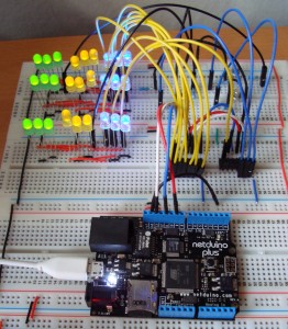
Putting it all together and wiring it up on breadboard gives you this:

Persistence Of Vision On Breadboard

Persistence Of Vision On Breadboard

Counting Using 74HC595 Shift Registers

Thursday, June 2nd, 2011

Following the post earlier this week regarding the implementation of a ShiftRegister class which allows the Netduino to control a series of 74HC595 shift registers I had a look at what would be needed to make the system count and show the output in binary on a series of LEDs. What you see here is the result. The hardware is the same as the previous post, only the software has changed.

One of the main desires is to allow the programmer to use the natural language features of C# to work with this class. The modifications should therefore support operations such as assignment, logical and etc. The main program loop for a counter should look something like this:

ShiftRegister shiftRegister = new ShiftRegister(16, Pins.GPIO_PIN_D9);
for (ushort index = 0; index < 10000; index++)
{
    shiftRegister = index;
    Debug.Print("Count: " + index + ", " + shiftRegister.ToString());
    shiftRegister.LatchData();
    Thread.Sleep(100);
}

In order to support this we will need to overload the implicit assignment operator for an unsigned short being assigned to a ShiftRegister instance. This results in the following code:

/// <summary>
/// Overload the assignment operator.
/// </summary>
/// <param name="usi">Unsigned short integer to assign to the register.</param>
/// <returns>New ShiftRegister holding the unsigned short value.</returns>
public static implicit operator ShiftRegister(ushort usi)
{
    ShiftRegister result = new ShiftRegister(16);   // ushorts are 16 bits.

    ushort mask = 1;
    for (int index = 0; index < 16; index++)
    {
        result._bits[index] = (usi & mask) > 0;
        mask <<= 1;
    }
    return (result);
}

This generates some problems with the base shift register class from the last post. Most noteably the creation of the SPI instance. The run-time system will generate an error should the programmer try and create two objects wanting to access the SPI bus. Reading the above code you can see that the assignment overload requires a new ShiftRegister instance to be created. A few changes are therefore required in order to allow the system to share the same interface. In order to allow this, the base class moves the SPI object from a shared instance to a static object. This ensures that only one of these can exist at any time. The remaining modifications to the class support this change and add a ToString() method for debugging. The modified code and a sample test project can be found here and the following video shows the application in action.

Further Developments

The base functionality assumed that the class is the only class wanting to use the SPI bus. The number of chips and breakout boards using is large and so it is likely that the programmer will want to communicate with several slave devices using the same bus. This is allowed using the SPI protocol and for the moment this is left as an exercise for the reader.

74HC595 Shift Registers

Monday, May 30th, 2011

The 7400 family of chips have for many years provided a set chips which implement common logic functions. The 74HC595 is a member of this family and provides an eight bit serial-in, parallel-out shift register. This register also provides a pin which can be used to cascade these chips providing a longer sequence of bits if required. In this post we will look at this chip and implement a C# class which can be used to set / reset individual bits in a series of cascaded shift registers. This is very much a software engineers view on how to access a shift register.

74HC595

Those of you who are familiar with the principles and operations of a shift register can skip the next section and move on the the implementation.

Shift Register Overview

A shift register in its simplest form is a series of bits. Data is shifted into the register using serial communication on bit at a time. Each time a bit is pushed into the shift register it moves all those to the right of it one place to the right with the bit at the end being discarded. For example, consider the following four bit register:

b3b2b1b0
1000

Adding a new bit with the value 0 results in the following:

b3b2b1b0Discarded
01000

The 74HC595 has an additional pin which allows the output of the discarded bit. By feeding this discarded bit into another 75HC595 you can build up a chain of cascaded chips to make a larger shift register.

Hardware

A simple LED driver is used to illustrate the hardware and software principles used. The hardware will use two 74HC595’s (although it is possible to use more) to drive a bank of LEDs (one per output for each chip). The bill of materials becomes:

ItemQuantityNotes
74HC5952
LEDs16One for each output pin on the 74HC595’s.
47 Ohm Resistor1
Netduino Plus1
WireLots of itYou really will need lot of it.

The LEDs are really there just to give an instant visual interpretation of the output from the shift registers and to prove the software is working. The way they are wired up and the resistor used to limit the current means that the more LEDs are powered, the dimmer they will be. The wiring looks something like this:
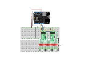
Shift Register Cascade

Shift Register Cascade

Looking at the diagram, the wiring seems confusing. The green wires show the wiring of the LEDs to the outputs of the shift registers. The outputs of the shift register should be wired to the LEDs from right to left in the order QA through QH. This is probably the most confusing part of the diagram due to the number of connections but these all follow the simple principle of wiring the output from the chip to the LED and then through to ground.

If we throw away the green connections then we have a few key connections:

  1. SI on the left most shift register (pin 14) should be connected to MOSI on the Netduino.
  2. SCK on the left most shift register (pin 11) should be connected to SPCK on the Netduino
  3. /G on the left shift register (pin 13) should be connected to the latch pin on the Netduino
  4. RCK on the left shift register (pin 12) should be connected to ground

When cascading the registers the following connections should be made for the registers to the right of the first register:

  1. Serial Out (pin 9) of the left chip to SI (pin 14) of the right chip
  2. SCK of both chips (pin 11) should be connected
  3. /G on both chips (pin 13) should be connected

The data is fed into the shift registers from the left with bit 0 appearing on the far right. The clock and the enable is fed into both chips at the same time. The serial data is fed into the chip on the far left and is cascaded on to the chip to it’s immediate right. Further chips can be added to the right and cascaded in the same manner. In this way, bit 0 will always be at the far right of the shift registers.

Software

The software used the SPI interface on the Netduino to communicate with the shift registers. An important note in the documentation is that the chip has a two stage process for transferring the data from the input to the output. Each bit is transferred into the shift register on the rising edge of the clock pulse. This is then transferred on to the output on the following rising edge. This is fine for all but the last bit as it will need a rising edge in order to be transferred to the output. Standard SPI has the idle clock set to low. As such this could lead to the final bit not being transferred to the output. In order to overcome this the SPI interface was set to the idle clock being high. The final transition from an active clock to an idle clock will then trigger the transfer of the final bit from the input to the output.

From a software engineers point of view a shift register is nothing more than an array of boolean values and this is the approach that was taken. The software holds an array of boolean values (multiples of 8 bits as the shift registers targeted are 8 bit registers). The software holds an array of values which the programmer can then choose to output to the registers.

The variable declarations become:

/// <summary>
/// Array containing the bits to be output to the shift register.
/// </summary>
private bool[] _bits;

/// <summary>
/// Number of chips required to implement this ShiftRegister.
/// </summary>
private int _numberOfChips;

/// <summary>
/// SPI interface used to communicate with the shift registers.
/// </summary>
private SPI _spi;
The variable holding the number of chips is used to help the runtime performance by not having to recalculate the number of chips on each transfer to the hardware.

The constructor for the class instantiates the array holding the number of bits in the shift register and the SPI interface:

public ShiftRegister(int bits, Cpu.Pin latchPin = Cpu.Pin.GPIO_Pin8, SPI.SPI_module spiModule = SPI.SPI_module.SPI1, uint speedKHz = 10)
{
    if ((bits > 0) && ((bits % 8 ) == 0))
    {
        _bits = new bool[bits];
        _numberOfChips = bits / 8;
        for (int index = 0; index < bits; index++)
        {
            _bits[index] = false;
        }

        SPI.Configuration config;

        config = new SPI.Configuration(SPI_mod: spiModule, ChipSelect_Port: latchPin, ChipSelect_ActiveState: false, ChipSelect_SetupTime: 0, ChipSelect_HoldTime: 0,  Clock_IdleState: true, Clock_Edge: false, Clock_RateKHz: speedKHz);

        _spi = new SPI(config);
    }
    else
    {
        throw new ArgumentOutOfRangeException("ShiftRegister: Size must be greater than zero and a multiple of 8 bits");
    }
}

A little bit operator overloading on the indexer allows the programmer to address the individual bit in the shift register:

/// <summary>
/// Overload the index operator to allow the user to get/set a particular 
/// bit in the shift register.
/// </summary>
/// <param name="bit">Bit number to get/set.</param>
/// <returns>Value in the specified bit.</returns>
public bool this[int bit]
{
    get
    {
        if ((bit >= 0) && (bit < _bits.Length))
        {
            return (_bits[bit]);
        }
        throw new IndexOutOfRangeException("ShiftRegister: Bit index out of range.");
    }
    set
    {
        if ((bit >= 0) && (bit < _bits.Length))
        {
            _bits[bit] = value;
        }
        else
        {
            throw new IndexOutOfRangeException("ShiftRegister: Bit index out of range.");
        }
    }
}

The final piece of the jigsaw is to allow the programmer to send the data to the shift register:

/// <summary>
/// Send the data to the SPI interface.
/// </summary>
public void LatchData()
{
    byte[] data = new byte[_numberOfChips];

    for (int chip = 0; chip < _numberOfChips; chip++)
    {
        data[chip] = 0;
        byte bitValue = 1;
        int offset = chip * 8;
        for (int bit = 0; bit < 8; bit++)
        {
            if (_bits[offset + bit])
            {
                data[chip] |= bitValue;
            }
            bitValue <<= 1;
        }
    }
    _spi.Write(data);
}

This method is really the work horse as it converts the bits into an array of bytes which are transferred to the shift registers.

Testing it Out

Testing should be easy, lets walk through all of the bits for a 16 bit register made by having two shift register connected together:

public static void Main()
{
    ShiftRegister shiftRegister = new ShiftRegister(16, Pins.GPIO_PIN_D9);
    while (true)
    {
        for (int index = 0; index < 16; index++)
        {
            shiftRegister[index] = true;
            shiftRegister.LatchData();
            Thread.Sleep(100);
            shiftRegister[index] = false;
        }
    }
}

This example uses two registers (16 bits) and uses pin D9 as the enable pin for the register. The code sets, displays and then resets each bit starting at bit 0 through to bit 15.

The full code for the shift register class can be found here (ShiftRegister.zip).
Home Computing

Saturday, May 7th, 2011

These guys take home computing to a whole new level:

Magic-1: Home brew CPU
Big Mess ‘o’ Wires

4 Digit, 7 Segment Display – Part 2 – Ouput an Unsigned Short

Tuesday, March 15th, 2011

Update 18 March 2011: This is where this series of posts finishes for the minute as I appear to have fried the MAX7219 (or something else is wrong with the setup) as I can send commands to it but the output does not make any sense. I’ll have to return to this series when I have a new chip.

This is the second in a series of posts discussing the MAX7219 LED driver chip being used to drive a four digit, seven segment LED display. The series is made up of the following posts:

  1. Part 1 – Output a Byte
    Output a series of bytes from the Netduino Plus using the SPI protocol
  2. Part 2 – Output an Unsigned Short (This Post)
    Similar to the first post but this time we will write a series of short integers using SPI. This will also start to implement the code which will write the data to the MAX7219 chip.
  3. Part 3 – Displaying Numbers
    Using the MAX7219 class to display a number on the display
  4. Part 4 – Displaying Sensor Data
    Hooking up a sensor to the Netduino and displaying the reading from the sensor.

Objective

The objective of this post is to start to flesh out the code (which will be presented in the final post) to start to send commands in the form of 16 bit unsigned shorts to the MAX7219.

All of the hardware remains as before and only the software changes. As before, the logic analyser is used to verify the results.

Software

The software required a minor update to convert the output to an array of ushorts and put the register in the msb and the data in the lsb.

Results

The main program does little more that send two commands to the logic analyser, namely a command to enter normal operation followed by a command to restrict the number of digits to four.

The results can be seen here:

This image shows the command to restrict the display to four digits being sent over the SPI bus.

The next step is to complete the wiring and to start to send display data to the MAX7219.

4 Digit, 7 Segment Display – Part 1 – Ouput a Byte

Tuesday, March 15th, 2011

Update 18 March 2011: This is where this series of posts finishes for the minute as I appear to have fried the MAX7219 (or something else is wrong with the setup) as I can send commands to it but the output does not make any sense. I’ll have to return to this series when I have a new chip 🙁

This series of posts will discuss using the MAX7219 LED driver chip to drive a four digit, seven segment LED display. The series is made up of the following posts:

  1. Part 1 – Output a Byte (This Post)
    Output a series of bytes from the Netduino Plus using the SPI protocol
  2. Part 2 – Output an Unsigned Short
    Similar to the first post but this time we will write a series of short integers using SPI. This will also start to implement the class which will write the data to the MAX7219 chip.
  3. Part 3 – Displaying Numbers
    Using the MAX7219 class to display a number on the display
  4. Part 4 – Displaying Sensor Data
    Hooking up a sensor to the Netduino and displaying the reading from the sensor.

Background Reading

The following posts provide some background information as these are similar projects:

Objective

The objective of these post is to connect the Netduino Plus to the breadboard and get a 5V logic signal representing a series of bytes. In order to do this it is necessary to convert the output from the Netduino Plus from 3.3V to 5V. I propose to experiment and use a 7408 quad 2 input AND gate to convert the 3.3V signal up to 5V. So for this post we will need the following components:

  1. Netduino Plus
  2. 1 x 74HCT08N quad 2 input AND gate
  3. Breadboard with 5V power supplied to the power rails
  4. Wire to connect the components

Theory

Part of this exercise is to see if we can convert a 3.3V signal into a 5V signal. This is necessary as the MAX7219 uses 5V inputs. The quad input AND gate was chosen to do this for no other reason than I had a few spare in the component box. The data sheet for this chip states that the minimum voltage for a high input is 3.15V when the chip is supplied with 4.5V. A quick experiment shows that a 3.3V input signal to this chip does indeed result in a high output.

So by connecting one of the inputs to the AND gate to 5V and the second to the signal source, then the output from the gate should reflect the input but translated from 3.3V to 5V.

One point to note is that the chip will take a little while for the signal on the inputs to be reflected on the output pins. This application will be running at a low frequency (10KHz) and so the chip should be able to keep up.

Software

The software is a simple starter program which cycles through the bytes from 0 to 255 and output’s these bytes on the SPI bus. The Saleae logic analyser is used to verify that the data is being output correctly. A small test program should demonstrate that the data is being transmitted on the bus correctly:

using System;
using System.Net;
using System.Net.Sockets;
using System.Threading;
using Microsoft.SPOT;
using Microsoft.SPOT.Hardware;
using SecretLabs.NETMF.Hardware;
using SecretLabs.NETMF.Hardware.NetduinoPlus;

namespace NetduinoPlusTestApplication
{
    public class Program
    {
        public static void Main()
        {
            SPI.Configuration config;
            SPI spi;
            byte[] b;

            config = new SPI.Configuration(Pins.GPIO_PIN_D10, false, 0, 0, false, false, 10, SPI.SPI_module.SPI1);
            spi = new SPI(config);
            b = new byte[1];

            while (true)
            {
                for (byte v = 0; v <= 255; v++)
                {
                    b[0] = v;
                    spi.Write(b);
                    Thread.Sleep(20);
                }
            }
        }
    }
}

Hardware

The following table shows how the Netduino Plus is connected to the 74HCT08N

74HCT08NConnection
2, 5, 10, 13, 14+5V
7Ground
12Netduino Plus digital pin 10 (used for CS)
1Netduino Plus digital pin 11 (MOSI)
4Netduino Plus digital pin 13 (Clock)

The ground on the Netduino Plus should also be connected to the ground on the breadboard.

Results

After completing the wiring the logic analyser was hooked up and the following trace appeared:

Scrolling through the trace show each of the ASCII characters being interpreted correctly.

So the next step it to start to build the class which will talk to the MAX7219.

NE555 Calculator and Data Logger

Saturday, March 5th, 2011

A while ago I wrote about my renewed relationship with the NE555 when I produced a simple astable circuit. The experience of trying to work out the values lead me to think about writing a calculator application. This lead me to wonder how I could validate the results given that I do not have an oscilloscope – simple add a data logger to the Netduino and use that. The following shows how I did it and provides some information about how the code works.

Objective

Write application which provides the functionality:

  1. Given a set of components and/or the frequency of the circuit calculate the missing value for the components or frequency
  2. Present the results to the user
  3. Capture data on the Netduino on one of the analog pins
  4. Transfer the data from the Netduino and plot the results

This will require two applications, one to interact with the user and perform the calculations and data plotting and one application to capture the data on the Netduino.

Netduino Application

This application is an extension to the Silverlight application which I documented here. This has the core functionality required to allow the Netduino Plus to communicate with a Silverlight application. A few slight changes were required, namely:

  1. Make the web server understand the commands which would be issued by the Silverlight application
  2. Implement a data logger.

For the first of the changes we simply need to add some additional variables to store the configuration and modify the ProcessCommand method. The system uses the Command.html special file (as before) to receive commands/requests from the user. The valid actions implemented are as follows:

ActionParametersDescription
tTest the connection. This simply returns a Hello string to the calling application.
gGet the preconfigured file and send this back to the caller.
cSampleRate and FileNameConfigure the Netduino data logger. The system will configure the Netduino to log data every SampleRate milliseconds and store the results in the specified file.

The last part of the change to the web server is to provide a mechanism to communicate the change to the data logging component. This done using an event as the data logger and the web server are executing in different threads.

The next change required is to implement the data logging functionality. The data logging runs in the main thread. The on board switch was used to trigger data collection rather than having the Netduino log data permanently. The on board LED was also used to indicate if the board is collecting data. A Timer was used to trigger the collection of data from the analog pin. This meant that the board can capture at most 1000 samples per second.

private static void onBoardButton_OnInterrupt(uint data1, uint data2, DateTime time)
{
    if (data2 == 0)
    {
        if (_logging)
        {
            _timer = null;
            _onBoardLED.Write(false);
            _logging = false;
        }
        else
        {
            using (TextWriter tw = new StreamWriter(@"SD" + _fileName, false))
            {
                tw.WriteLine("Ticks,Data");
                tw.Close();
            }
            _startTime = Utility.GetMachineTime().Ticks;
            _timer = new Timer(new TimerCallback(CollectData), null, 0, _sampleRate);
            _onBoardLED.Write(true);
            _logging = true;
        }
    }
}

This code is tied to the on board switches interrupt. It starts and stops the logging depending upon the current state. A logging start request opens the specified file and puts the header into the file. This effectively deletes and results already stored in the file. The timer is created and tied to the CollectData callback. This callback simply reads the pin and writes the number of ticks since the start of the logging session along with the reading from the pin.

private static void CollectData(object o)
{
    string data;

    data = Utility.GetMachineTime().Ticks - _startTime + "," + _analogInput.Read();
    using (TextWriter tw = new StreamWriter(@"SD" + _fileName, true))
    {
        tw.WriteLine(data);
        tw.Close();
    }
}

Silverlight Application

This is where the project began to take on a life of it’s own. The code discussed here consumed the majority of the time spent on the project. The code is fairly well commented and so the main features will be discussed here.

The project uses MVVM to implement a calculator for the NE555. This results in little code in the code behind for the main page. What code there is simply creates a new instance of the View Model class and calls methods in the class when buttons on the interface are clicked. The remaining communication is achieved using data binding in Silverlight.

The calculator can be used to calculate one of the following (given the remaining three values):

  • R1
  • R2
  • C1
  • F

The system takes three of the specified values and calculates the remaining. The values for the components can come from three sources, a standard component, a user specified value or a range of values.

If single component values are used (either standard components or user values) then a single result set is generated. If a range of values are selected for one or more of the components then the system will generate a table of values with one line for each of the requested values.

So much for discussing the application, it is probably just as easy to try the application which can be found here.

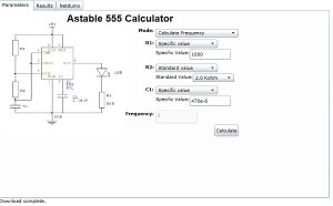
The first tab (Parameters on the application collects the parameters for the calculations and allows the user to request that the results are calculated.

NE555 Calculator

NE555 Calculator

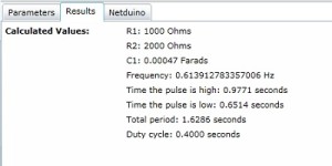
The next tab (Results) presents the results of the calculation.

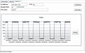
The final tab (Netduino) allows the application to communicate with a Netduino Plus.

NE555DataLogger

Although the Silverlight application is hosted on my web site, you can still use this to communicate with your Netduino Plus if it is connected to your network.

Results

The resulting application is more or less complete. There are a few things which could be done to make it more robust or more useful, namely:

  1. Add data validation to the properties in the NE555Calculator class.
  2. Make the data logger work with multiple files.
  3. Allow the configuration of the pin used to collect data.
  4. Use the date and time to record when the sample was taken
  5. Collect multiple samples at the same time
  6. Allow the user to enter the reference voltage and scale the data items plotted accordingly
  7. Convert the ticks into milliseconds

These are left as an exercise for the reader.

Source Files

The source files for this project can be found here:

SimpleWebServer.zip

Astable NE555 Silverlight Calculator

As usual, these sources are provided as is and without warranty. They are used at your own risk.

Setting This Up

The Silverlight application can be run from a web site or from Visual Studio. The web server needs a little more than just running the project on the Netduino. You will also have to place the clientaccess.xml policy file on the SD card as Silverlight requests this file in order to determine if it allowed to talk to the web server.

Saleae Logic Analyser Has Arrived

Saturday, March 5th, 2011

I’ve been considering getting one of these for a while and it finally arrived today. First impressions, well packed sturdy and smaller than I thought it would be. The software installed without a hitch. Powered up and connected to the Netduino to check it works.

A little test program:

OutputPort output = new OutputPort(Pins.GPIO_PIN_D0, false);
SerialPort com2 = new SerialPort(SerialPorts.COM2, 9600, Parity.None, 8, StopBits.One);

com2.Open();
while (true)
{
    output.Write(true);
    Thread.Sleep(10);
    output.Write(false);
    Thread.Sleep(10);
    com2.Write(Encoding.UTF8.GetBytes("Hello, world"), 0, 12);
}

It took longer to write the test program than to install the software and hook up the analyser.

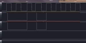
And some results:

Well, the first program everyone writes has to say “Hello, world” – well it does if you are an old C programmer anyway.

Flashing LED Using an Astable 555

Sunday, February 20th, 2011

This project will use the 555 timer IC to flash an LED with the eventual aim of using the timer to provide a regular timing pulse.

Objective

Use the 555 timer to flash an LED with a period of 1 second.

Components

The timer being used is a standard NE555N timer. This is a cheap general purpose timer circuit and has been around for many years. In fact I remember using them when I first became interested in electronics at school.

The circuit for setting this chip up in astable mode is as follows:

So along with the chip itself we will need 3 resistors, 2 capacitors and an LED. Thye values of R1, R2 and C1 determine the frequency of the pulses according to the following equation:

A frequency of 1 Hz was chosen to make the pulses clearly visible to the observer. A little reordering of the equation and a sift through some standard components gave the following values for these components:

Component Value
R1 1 KOhm
R2 2 KOhms (two 1 KOhm resistors in series)
C1 470 micro Farad

Putting it all together

Gathering all of the components together along with some breadboard gave a LED flashing at approximately 1 Hz. I say approximately as I’ll need to feed that output through a logic analyser / oscilloscope to verify the exact frequency.

Analog Input

Saturday, February 12th, 2011

The aim of this experiment was to test the analog input.  The simplest way I could think of to do this is to hook up a potentiometer to one of the analog pins and then display the values using the debugger.

First task is to wire up the board.  The final wiring looked like this:

I say final wiring as my initial version looked a little different.  The first version did not have the 3.3V output connected to Aref and as a result I found myself getting very odd results from the analog input pin.

The code to read data from the Netduino looks like the following:

public static void Main()
{
    AnalogInput analog;

    analog = new AnalogInput(Pins.GPIO_PIN_A1);
    analog.SetRange(0, 1023);
    while (true)
    {
        Debug.Print(analog.Read().ToString());
        Thread.Sleep(1000);
    }
}

Running the application and turning the potentiometer results in a range of values from 0 to 1023.