NETMF Timers
January 6th, 2013 • Netduino, Software Development • 4 Comments »A few days ago in the Netduino chat room we were discussing a problem with the Timer class. Should be a simple problem to solve as I had used timers in .NET applications many times. A short while later it became obvious that the Timer class was not as easy to use as I thought. In this post we will look at the NETMF implementation of the Timer class and how it can be used.
In all of the examples below I will be working on a 50% duty cycle. So a 100 Hertz signal should be 10ms between the rising edges of the signal where the signal will be high for 5ms followed by low for 5ms.
All of the following examples will run on the Netduino Plus 2.
Setting up a Simple Timer
The basic timer constructor takes four parameters:
- Callback
- User defined object
- Delay
- Period
Callback
The Callback parameter is a TimerCallback object. This will be called by the Timer at the period defined by the period parameter.
User defined object
This is an object defined by the user and can be used to identify the source of the callback. Initially we will be setting this to null as we will not be using it.
Delay
The number of milliseconds to pause before the callback method is called.
Period
Period (in milliseconds) between invocations of the Callback method.
So now we know how this should work, let’s jump in with a simple example. Here we will generate a 100Hz signal and we will start the timer immediately. The code for this will look like this:
using System;
using System.Threading;
using Microsoft.SPOT.Hardware;
using SecretLabs.NETMF.Hardware.Netduino;

namespace BasicTimer
{
    public class Program
    {
        private static Timer oneHundredHertzTimer = null;
        private static OutputPort oneHundredHertzPulse = null;
        private static TimerCallback timerCallback = null;
        private static OutputPort trigger = null;

        public static void Main()
        {
            trigger = new OutputPort(Pins.GPIO_PIN_D1, false);
            timerCallback = new TimerCallback(TimerInterrupt);
            oneHundredHertzPulse = new OutputPort(Pins.GPIO_PIN_D7, false);
            trigger.Write(true);
            trigger.Write(false);
            oneHundredHertzTimer = new Timer(timerCallback, null, 0, 5);
            Thread.Sleep(Timeout.Infinite);
        }

        private static void TimerInterrupt(object state)
        {
            oneHundredHertzPulse.Write(!oneHundredHertzPulse.Read());
        }
    }
}
The trigger pin is simply used to indicate the start of the program run. This is used to allow the logic analyser to start data capture.
If we hook up the logic analyser we should get a trace which looks something like the following:
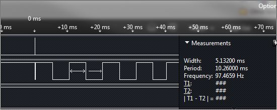
Basic Timer
The top trace shows the trigger pulse whilst the trace below shows the output from the timer callback. If we expand the start of the trace we see the following:
Timer with trigger
As you can see, there is a small pulse (the trigger) at the start followed by the pulses generated by the timer. The timer between the falling edge of the trigger and the rising edge of the first pulse generated by the timer is approximately 16us. This can be put down to the amount of time it takes for the NETMF instructions to complete the construction of the timer. So the first thing the timer does is to invoke the callback method defined in the constructor.
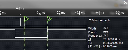
If we modify the construction of the timer slightly we can see the impact of the delay parameter. Let’s change the construction to the following:
oneHundredHertzTimer = new Timer(timerCallback, null, 50, 5);
If we run this application (see the project BasicTimerWithDelay) we will see the following in the logic analyser:
As you can see, the start of the timer has been delayed by 50ms.
Two Timers, One Interrupt
In this example we will look at the role the user defined object has in the TimerCallback parameter. This object can be used to allow the system to use a single callback from multiple timers. The object can be used to determine which timer invoked the callback.
The user defined object is an instance of an object which is passed to the callback method when it is called. In the following we start with an enum:
private enum TimerState { OneHertz, TwoHertz };
Now when we create the timers we create a new object and pass this into the constructor. Our constructors look like the following:
TimerState oneHertzState = TimerState.OneHertz;
oneHertzTimer = new Timer(timerCallback, oneHertzState, 0, 500);
TimerState twoHertzState = TimerState.TwoHertz;
twoHertzTimer = new Timer(timerCallback, twoHertzState, 0, 250);
for the two hertz timer.
As you can see, both timers have the same method being invoked as the callback method. However, each timer will pass in a different object (albeit of the same type) to the callback method. We can then use this parameter to determine the action we should take. The code for the callback method will look like the following:
private static void TimerInterrupt(object state)
{
	switch ((TimerState) state)
	{
		case TimerState.OneHertz:
			oneHertzPulse.Write(!oneHertzPulse.Read());
			break;
		case TimerState.TwoHertz:
			twoHertzPulse.Write(!twoHertzPulse.Read());
			break;
	}
}
The full application is as follows:
using System;
using System.Threading;
using Microsoft.SPOT.Hardware;
using SecretLabs.NETMF.Hardware.Netduino;

namespace TimerExample
{
    public class Program
    {
        private static Timer oneHertzTimer = null;
        private static OutputPort oneHertzPulse = null;

        private static Timer twoHertzTimer = null;
        private static OutputPort twoHertzPulse = null;

        private static TimerCallback timerCallback = null;

        private enum TimerState { OneHertz, TwoHertz };

        private static OutputPort trigger = null;

        public static void Main()
        {
            trigger = new OutputPort(Pins.GPIO_PIN_D1, false);
            timerCallback = new TimerCallback(TimerInterrupt);
            trigger.Write(true);
            trigger.Write(false);
            //
            //  Set up the one hertz timer.
            //
            oneHertzPulse = new OutputPort(Pins.GPIO_PIN_D7, false);
            TimerState oneHertzState = TimerState.OneHertz;
            oneHertzTimer = new Timer(timerCallback, oneHertzState, 0, 500);
            //
            //  Set up the two hertz timer.
            //
            twoHertzPulse = new OutputPort(Pins.GPIO_PIN_D6, false);
            TimerState twoHertzState = TimerState.TwoHertz;
            twoHertzTimer = new Timer(timerCallback, twoHertzState, 0, 250);
            //
            Thread.Sleep(Timeout.Infinite);
        }

        private static void TimerInterrupt(object state)
        {
            switch ((TimerState) state)
            {
                case TimerState.OneHertz:
                    oneHertzPulse.Write(!oneHertzPulse.Read());
                    break;
                case TimerState.TwoHertz:
                    twoHertzPulse.Write(!twoHertzPulse.Read());
                    break;
            }
        }
    }
}
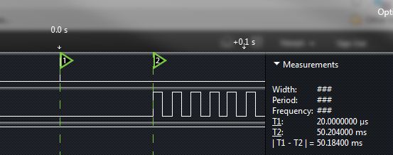
If we run this application we will see the following on the logic analyser:
Two timers with one interrupt.
As you can see, we are generating a one and a two hertz signal using a single callback.
Stopping A Timer
So far we have considered starting a timer and the various options for delaying and callbacks. There will come a point where we will want to stop a timer from executing. A quick glance through the methods provided for the Timer class reveals that there is no method do do this. In this scenario, the first instinct is to simply set the variable referencing to the object to null.
So if we take the first example as out starting point we will add a small amount of code to deal with a button press. The idea is that when the user presses the onboard button on the Netduino Plus 2, the application will terminate the timer by setting to timer object to null. The code becomes:
using System.Threading;
using Microsoft.SPOT.Hardware;
using SecretLabs.NETMF.Hardware.Netduino;
using Microsoft.SPOT;

namespace StoppingATimer
{
    public class Program
    {
        private static Timer oneHundredHertzTimer = null;
        private static OutputPort oneHundredHertzPulse = null;
        private static TimerCallback timerCallback = null;
        private static InterruptPort button = null;

        public static void Main()
        {
            timerCallback = new TimerCallback(TimerInterrupt);
            oneHundredHertzPulse = new OutputPort(Pins.GPIO_PIN_D7, false);
            button = new InterruptPort(Pins.ONBOARD_BTN, true, Port.ResistorMode.PullUp, Port.InterruptMode.InterruptEdgeHigh);
            button.OnInterrupt += new NativeEventHandler(button_OnInterrupt);
            oneHundredHertzTimer = new Timer(timerCallback, null, 0, 5);
            Thread.Sleep(Timeout.Infinite);
        }

        private static void button_OnInterrupt(uint data1, uint data2, System.DateTime time)
        {
            oneHundredHertzTimer = null;
            Debug.Print("Timer set to null.");
        }

        private static void TimerInterrupt(object state)
        {
            oneHundredHertzPulse.Write(!oneHundredHertzPulse.Read());
        }
    }
}
If you deploy this application to the Netduino Plus 2 you will see the same output (on the logic analyser) as the first example in this post. Namely, a 100Hz square wave with a 50% duty cycle.
So the next thing to try is pressing the button and see what happens. If everything works as expected then the timer should be set to null and the timer should terminate. So let’s press the button and start the logic analyser.
And the timer keeps on running. In order to kill the timer we must ensure that it is disposed of correctly. We can do this by modifying the button interrupt method as follows:
private static void button_OnInterrupt(uint data1, uint data2, System.DateTime time)
{
	oneHundredHertzTimer.Dispose();
	oneHundredHertzTimer = null;
	Debug.Print("Timer set to null.");
}
Running the application again and pressing the button results in the expected behaviour.
Changing the Frequency
In our final example we will look at changing the frequency of the timer. This example uses the button press interrupt from the previous example but this time it will halve the period (i.e. double the frequency of the output signal) of the timer. The application uses the Change method to change the timer on the fly. So let’s dive straight in with some code:
using System.Threading;
using Microsoft.SPOT.Hardware;
using SecretLabs.NETMF.Hardware.Netduino;
using Microsoft.SPOT;

namespace ChangingTheFrequency
{
    public class Program
    {
        private static Timer frequencyGenerator = null;
        private static OutputPort frequencyGeneratorOutput = null;
        private static TimerCallback timerCallback = null;
        private static InterruptPort button = null;
        private static int currentPeriod;

        public static void Main()
        {
            timerCallback = new TimerCallback(TimerInterrupt);
            frequencyGeneratorOutput = new OutputPort(Pins.GPIO_PIN_D7, false);
            button = new InterruptPort(Pins.ONBOARD_BTN, true, Port.ResistorMode.PullUp, Port.InterruptMode.InterruptEdgeHigh);
            button.OnInterrupt += new NativeEventHandler(button_OnInterrupt);
            currentPeriod = 500;
            frequencyGenerator = new Timer(timerCallback, null, 0, currentPeriod);
            Thread.Sleep(Timeout.Infinite);
        }

        private static void button_OnInterrupt(uint data1, uint data2, System.DateTime time)
        {
            if (currentPeriod > 100)
            {
                currentPeriod /= 2;
                frequencyGenerator.Change(0, currentPeriod);
            }
        }

        private static void TimerInterrupt(object state)
        {
            frequencyGeneratorOutput.Write(!frequencyGeneratorOutput.Read());
        }
    }
}
As you can see the code is relatively straight forward. Connecting up the logic analyser and running the application generates a 1 Hz signal (500ms period will result in 1Hz). Pressing the button on the Netduino Plus 2 will cause the period to be halved and hence the frequency to be doubled. You logic analyser will confirm this, I know mine did.
One thing you should note is that the Change method returns a value to indicate if the method has disposed of the old timer. I have never seen this not return true but if you see some odd behaviours with timers still generating interrupts at old frequencies then it may be the result of an old timer still hanging around.
Conclusion
This article was inspired by a posting on the Netduino chatrooms regarding the changing/killing of timers. I must admit I was a little astounded to find that there was no Stop or Start method in the class. As you can see, the techniques for doing this are not complex, they are just not obvious.
There are also some nice feature, like the fact that Timers run in their own threads. Investigation of these features are left as an exercise for the reader.
As always, the Source code is available for download.


