Simple GPIO – The Way of the Register
If you have been following this blog for a while you will be aware that I have recently changed the way I write code for the STM8S from using the STD Peripheral Library to using direct register access. This has required that I go back to basics learning a new way to perform tasks I had only just mastered. The Way of the Register posts will show you have to control the STM8 using register access.
This first post will look at a simple task, controlling GPIO lines. The aim of this first exercise is to simply toggle one of the GPIO lines.
Hardware
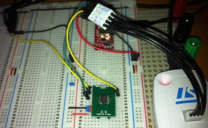
For this task we need very little hardware, only the STM8S set up on breadboard. For this we need a minimum of two capacitors and the chip itself. A 1uF capacitor is placed between VSS and VCAP and a 100 nF capacitor is placed between VDD and VSS. An additional 1uF capacitor is also placed across the +3.3V and ground of the power supply. The following shows this set up on breadboard along with the breadboard power supply, connections to the oscilloscope and the ST-Link programmer:
The Registers
Before we can start coding we need to have a look at the registers we will be using. The GPIO pins have five registers used to control the GPIO function and set/read the value of a pin. These are:
| Register |
|---|
| Data Direction Register |
| Control Register 1 |
| Control Register 2 |
| Output Data Register |
| Input Data Register |
The following sections provide a brief description of the registers. For more information you should consult RM0016 – STM8S Reference Manual.
Px_DDR – Data Direction Register
This register determines which or the GPIO pins are outputs and which are inputs. A value of one in a bit sets a port line to output and zero sets the port line to input. You can set the value of the whole register or each individual bit in the register.
To set the whole register in one go you would execute something like the following:
PD_DDR = 0x0f;
This sets bits 0-3 inclusive of port D to output whilst bit 4-7 are inputs.
An alternative to this is to set up each GPIO pin individually, so the equivalent of the above is:
PD_ODR = 0;
PD_DDR_DDR0 = 1;
PD_DDR_DDR1 = 1;
PD_DDR_DDR2 = 1;
PD_DDR_DDR3 = 1;
Px_CR1 & PxCR2 – Control Register 1 and 2
These two registers determine the properties of the pins depending upon the operating mode of the pin. The following table summarises the operating modes:
| Register | Mode | Value | Description |
|---|---|---|---|
| CR1 | Input | 0 | Floating input |
| CR1 | Input | 1 | Input with pull-up |
| CR1 | Output | 0 | Open drain |
| CR1 | Output | 1 | Push-Pull |
| CR2 | Input | 0 | Interrupt disabled |
| CR2 | Input | 1 | Interrupt enabled |
| CR2 | Output | 0 | Output up to 2 MHz. |
| CR2 | Output | 1 | Output up to 10 MHz |
In our case, we need the output pin to operate in Push-Pull mode and as we do not know the final speed of the output signal we will set this to the maximum, 10 MHz.
As with the data direction register, each bit in the registers maps to a specific GPIO on each port. In the case of these registers the bits are labelled C10-C17 (for Control Register 1) and C20-C27 (for control Register 2). The format appears to be CRB, where C stands for Control Register; R is an integer representing the register number and B is an integer representing the bit to be set.
In our case, this results in the following code:
PD_CR1_C14 = 1;
PD_CR2_C24 = 1;
Px_ODR – Input/Output Data Registers
These two registers allow you to read the value of an input pin and set the value of an output pin. As with the previous registers you can set/read the register in its entirety or bit by bit. So to turn all of the outputs off you would execute something like:
PD_ODR = 0;
In the case we have been using we will be outputting data on pin 4 of port D. So to set the pin high you would execute the following statement:
PD_ODR_ODR4 = 1;
Software
Now we have the theory in place lets put together a simple application which uses it. The following code sets up port D to have pin 4 configured as an output operating to 10 MHz. The main program loop then simply keeps flipping the bit. The result should be a square wave signal.
#include <iostm8S103f3.h>

int main( void )
{
    //
    //  Initialise Port D.
    //
    PD_ODR = 0;             //  All pins are turned off.
    PD_DDR_DDR4 = 1;        //  Port D, bit 4 is output.
    PD_CR1_C14 = 1;         //  Pin is set to Push-Pull mode.
    PD_CR2_C24 = 1;         //  Pin can run upto 10 MHz.
    //
    //  Now lets toggle to IO line.
    //
    while (1)
    {
        PD_ODR_ODR4 = 1;    // Turn Port D, Pin 4 on.
        PD_ODR_ODR4 = 0;    // Turn Port D, Pin 4 off.
    }
}
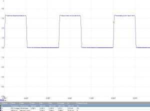
If we hook an oscilloscope up to PD4 on the STM8 chip we see the following:
As you can see, we have a square wave. Note that the wave is not symmetrical. This is due to the branch instruction being executed in the while loop to go back to the start of the loop.
Source Code
Here is the IAR project and source code for this post. This code has been tested on my reference platform, Variable Lab Protomodule and the STM8S Discovery board.
Compatibility
| System | Compatible? |
| STM8S103F3 (Breadboard) | |
| Variable Lab Protomodule | |
| STM8S Discovery |
Tags: Electronics, Software Development, STM8, The Way of the Register
Sunday, July 8th, 2012 at 9:23 am • Electronics, Software Development, STM8 • RSS 2.0 feed Both comments and pings are currently closed.


