September 12th, 2013 • Electronics, STM8 • Comments Off on Storing Data in EEPROM on the STM8S
During a recent project it became desirable to store a small amount of data in some non-volatile memory in order that the system state could be restored following loss of power. This article demonstrates how to achieve this by writing a small amount of data to the data EEPROM of the STM8S105Cr micro-controller on the STM8S Discovery board.
Memory Layout, Access and Protection
The Data EEPROM area of the STM8S series of micro-controllers varies depending upon the specific unit being used. For this article the specific micro-controller being used is the STM8S105C6 on the STM8S Discovery board. This micro-controller has 1KByte of EEPROM in the address range 0x4000 – 0x43ff.
By default the data area is write protected and cannot be modified by the main program. The write protection is removed by using a key to unlock the EEPROM data area. The flash program area is similarly protected but we will only consider the data EEPROM area. In order to write to the EEPROM area the application will need to write two security keys called Memory Access Security System (MASS) keys to the FLASH_DUKR register. These keys will unlock the EEPROM area and allow the application to write data to the EEPROM until the application turns write protection back on.
The MASS keys for the data EEPROM area are:
0xae
0x56
The algorithm for enabling write access to the EEPROM data area is as follows:
Check the DUL bit of FLASH_IASPR. If this bit is set then the data area is writeable and no further action is required.
Write the first MASS key (0xae) to the FLASH_DUKR register.
Write the second MASS key (0x56) to the FLASH_DUKR register.
At the end of the process of successfully writing the MASS keys the DUL bit of the FLASH_IASPR register will be set. This bit will remain set until either the application changes the bit or the micro-controller is reset. Resetting the DUL bit programatically reinstates the write protection for the EEPROM memory.
Read-while-write (RWW)
This feature is not available on all of the STM8S family of processors and you should consult the data sheet for the unit being used if you are interested in using this feature. The RWW feature allows the program memory to be read whilst the EEPROM memory is being written to.
Byte Programming
Byte level programming is available for both the program memory and the EEPROM memory. To use this feature the application simply needs to unlock the EEPROM using the MASS keys and then write individual bytes into the EEPROM memory. To erase a byte simply write 0x00 into the memory location.
Word and Page Programming
The STM8S also allows word (4 bytes) and block programming. Both of these are faster than byte programming and block programming is faster than word programming. These features will not be discussed further here and are mentioned simply for awareness.
Interrupts
The system can be configured to generate an interrupt for the following event:
Successful write operation.
Successful erase operation.
Illegal operation (writing to protected pages).
Interrupts are enabled by setting FLASH_CR1_IE to 1. When this bit is set, an interrupt will be generated when the FLASH_IASPR_EOP or FLASH_IASPR_WR_PG_DIS bits are set.
Software
The original aim of the software was to write a small amount of data to the data EEPROM of the STM8S and use the ST Visual Programmer to verify that the memory contents had changed. As the project progressed it became apparent that we would also need some code to verify the data.
Writing the Data
The application to write data to the EEPROM is relatively simple:
//
//  Write a series of bytes to the EEPROM of the STM8S105C6.
//
//  This software is provided under the CC BY-SA 3.0 licence.  A
//  copy of this licence can be found at:
//
//  http://creativecommons.org/licenses/by-sa/3.0/legalcode
//
#if defined DISCOVERY
    #include <iostm8S105c6.h>
#else
    #include <iostm8s103f3.h>
#endif

//
//  Data to write into the EEPROM.
//
unsigned int _pulseLength[] = { 2000U, 27830U, 400U, 1580U, 400U, 3580U, 400U };
unsigned char _onOrOff[] =    {   1,      0,     1,     0,    1,     0,    1 };
char numberOfValues = 7;

//--------------------------------------------------------------------------------
//
//  Write the default values into EEPROM.
//
void SetDefaultValues()
{
    //
    //  Check if the EEPROM is write-protected.  If it is then unlock the EEPROM.
    //
    if (FLASH_IAPSR_DUL == 0)
    {
        FLASH_DUKR = 0xae;
        FLASH_DUKR = 0x56;
    }
    //
    //  Write the data to the EEPROM.
    //
    char *address = (char *) 0x4000;        //  EEPROM base address.
    *address++ = (char) numberOfValues;
    for (int index = 0; index < numberOfValues; index++)
    {
        *address++ = (char) (_pulseLength[index] & 0xff);
        *address++ = (char) ((_pulseLength[index] >> 8) & 0xff);
        *address++ = _onOrOff[index];
    }
    //
    //  Now write protect the EEPROM.
    //
    FLASH_IAPSR_DUL = 0;
}

//--------------------------------------------------------------------------------
//
//  Main program loop.
//
void main()
{
    SetDefaultValues();
}
The application simply enables writing to the EEPROM and then writes data to the memory. It also re-enables the write protection at the end of the write operation.
Verifying the Data
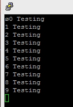
Testing this application should simply be a case of creating a new project, putting the above in main.c, setting some options and then running the code. The EEPROM data can then be read by ST Visual Develop and verified by hand. After compiling and executing the above code, start ST visual Programmer, connect it to the STM8S Discovery board and download the contents of the EEPROM:
This does not look correct. Double checking the code against RM0016 – Reference Manual all looks good with the application. So try downloading the EEPROM data again:
This time the data looks good and the values appear to be correct.
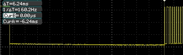
Downloading the EEPROM data again gave the first set of results. Trying for a fourth thime gave the second set of results. It appears that the correct data is only retrieved every second attempt (for reference, I am using ST Visual Develop version 3.2.8 on Windows 8).
At this point I decided that the only way to ensure that the data is in fact correct is to write a verification method into the code. The new application becomes:
//
//  Write a series of bytes to the EEPROM of the STM8S105C6 and then
//  verify that the data has been written correctly.
//
//  This software is provided under the CC BY-SA 3.0 licence.  A
//  copy of this licence can be found at:
//
//  http://creativecommons.org/licenses/by-sa/3.0/legalcode
//
#if defined DISCOVERY
    #include <iostm8S105c6.h>
#else
    #include <iostm8s103f3.h>
#endif

//
//  Data to write into the EEPROM.
//
unsigned int _pulseLength[] = { 2000U, 27830U, 400U, 1580U, 400U, 3580U, 400U };
unsigned char _onOrOff[] =    {   1,      0,     1,     0,    1,     0,    1 };
char numberOfValues = 7;

//--------------------------------------------------------------------------------
//
//  Write the default values into EEPROM.
//
void SetDefaultValues()
{
    //
    //  Check if the EEPROM is write-protected.  If it is then unlock the EEPROM.
    //
    if (FLASH_IAPSR_DUL == 0)
    {
        FLASH_DUKR = 0xae;
        FLASH_DUKR = 0x56;
    }
    //
    //  Write the data to the EEPROM.
    //
    char *address = (char *) 0x4000;        //  EEPROM base address.
    *address++ = (char) numberOfValues;
    for (int index = 0; index < numberOfValues; index++)
    {
        *address++ = (char) (_pulseLength[index] & 0xff);
        *address++ = (char) ((_pulseLength[index] >> 8) & 0xff);
        *address++ = _onOrOff[index];
    }
    //
    //  Now write protect the EEPROM.
    //
    FLASH_IAPSR_DUL = 0;
}

//--------------------------------------------------------------------------------
//
//  Verify that the data in the EEPROM is the same as the data we
//  wrote originally.
//
void VerifyEEPROMData()
{
    PD_ODR_ODR2 = 1;            //  Checking the data
    PD_ODR_ODR3 = 0;            //  No errors.
    //
    char *address = (char *) 0x4000;        //  EEPROM base address.
    if (*address++ != numberOfValues)
    {
        PD_ODR_ODR3 = 1;
    }
    else
    {
        for (int index = 0; index < numberOfValues; index++)
        {
            unsigned int value = *address++;
            value += (*address++ << 8);
            if (value != _pulseLength[index])
            {
                PD_ODR_ODR3 = 1;
            }
            if (*address++ != _onOrOff[index])
            {
                PD_ODR_ODR3 = 1;
            }
        }
    }
    PD_ODR_ODR2 = 0;        // Finished processing.
}

//--------------------------------------------------------------------------------
//
//  Setup port D for data output.
//
void SetupPorts()
{
    //
    //  Initialise Port D.
    //
    PD_ODR = 0;             //  All pins are turned off.
    PD_DDR = 0xff;          //  All bits are output.
    PD_CR1 = 0xff;          //  All pins are Push-Pull mode.
    PD_CR2 = 0xff;          //  Pins can run up to 10 MHz.
}

//--------------------------------------------------------------------------------
//
//  Main program loop.
//
void main()
{
    SetupPorts();
    SetDefaultValues();
    VerifyEEPROMData();
}
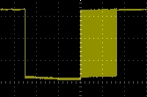
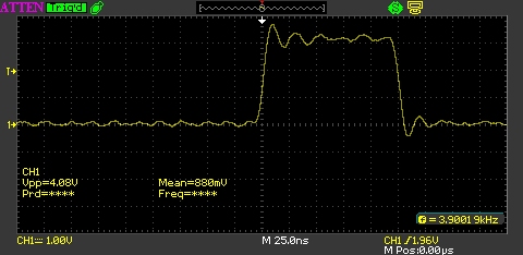
The application uses Port D, pins 2 and 3 to indicate how the verification is proceeding. Pin D2 goes high when the application is verifying the data. Pin D3 is used to indicate if an error is found. Compiling the above and connecting up a scope gives the following output:
Pin D2 is connected to the yellow channel and pin D3 is connected to the blue channel. The above shows that the verification process starts and no errors are generated.
Conclusion
There may only be a small amount of EEPROM storage space available on the STM8S (640 bytes to be precise) but this offers a quick and simple method of storing data which may be needed between system resets/power loses.
In it’s simplest form, the code required to store the data is trivial only requiring the developer to enable the write operations and then disable after the data has been written successfully.
In addition to the above I would recommend that some form of checksum value is written into the EEPROM as it is possible that the power is lost as the data is being written into the EEPROM. In this case there are two arrays being written and we may only have written half of the data when the power is lost. This is left as an exercise for the reader.
I considered two methods of modulating the signal:
Software implementation using a timer
Hardware implementation using PWM
The software implementation is attractive as it does not require the addition of any additional components to the circuit and hence reduces the cost of the remote control. On the downside, this requires a slightly more complex implementation and may cause some issues due to the timing of the interrupts.
Using PWM is a much simpler software solution as it only requires that the timers are setup correctly and turned on at the right time.
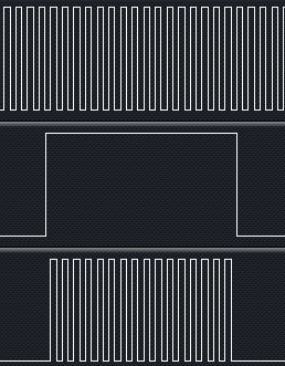
How Does Modulation Work?
Modulation works by combining a clock frequency (in the case of infra-red this is normally around 38KHz – 40 KHz) with a digital signal. When the digital signal is supposed to be at logic 1 then the clock signal is output rather than a stable logic level 1. When the signal is at logic level 0 then no signal is generated. The following illustrates this:
Digital signal:
Digital Signal
Clock signal:
38.4KHz Clock Signal
Combined output:
Digital Signal And Clock
In the final image above, the top trace shows the clock signal, the middle trace shows the digital signal we wish to generate and the lower trace shows the signal which should be output by the circuit.
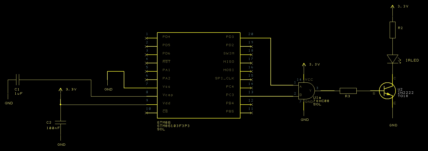
Hardware Changes
The hardware solution requires the combination of a digital signal with a PWM signal. The easiest way to do this is to use a single AND gate taking input from the digital output required and a clock signal.
Nikon Remote Circuit With Added Modulation
Searching the RS Components web site lead to a single and gate component for a small price. This would be ideal for solving this problem.
Software Changes
The software changes are minimal as we simply need to configure a timer and turning it on and off as required. We will be using Timer 1, Channel 4 configured to generate a 38.4KHz PWM signal.
Setup
A 38.4KHz signal has a peak to peak duration of 26uS The system is running at 2MHz and so we would need a count value of 52 clock pulses (with no prescalar applied). Using Timer 2, Channel 4 results in the following setup code:
//--------------------------------------------------------------------------------
//
//  Set up Timer 1, channel 4 to output a single pulse lasting 240 uS.
//
void SetupTimer1()
{
    TIM1_ARRH = 0x00;       //  Reload counter = 51
    TIM1_ARRL = 0x33;
    TIM1_PSCRH = 0;         //  Prescalar = 0 (i.e. 1)
    TIM1_PSCRL = 0;
    //
    //  Now configure Timer 1, channel 4.
    //
    TIM1_CCMR4_OC4M = 7;    //  Set up to use PWM mode 2.
    TIM1_CCER2_CC4E = 1;    //  Output is enabled.
    TIM1_CCER2_CC4P = 0;    //  Active is defined as high.
    TIM1_CCR4H = 0x00;      //  26 = 50% duty cycle (based on TIM1_ARR).
    TIM1_CCR4L = 0x1a;
    TIM1_BKR_MOE = 1;       //  Enable the main output.
}
Timer 2 Interrupt Handler
A minor change to the Timer 2 interrupt handler is required to turn off Timer 1 when the signal is no longer being generated:
//--------------------------------------------------------------------------------
//
//  Timer 2 Overflow handler.
//
#pragma vector = TIM2_OVR_UIF_vector
__interrupt void TIM2_UPD_OVF_IRQHandler(void)
{
    _currentPulse++;
    if (_currentPulse == _numberOfPulses)
    {
        //
        //  We have processed the pulse data so stop now.
        //
        PD_ODR_ODR3 = 0;
        TIM2_CR1_CEN = 0;
        TIM1_CR1_CEN = 0;           //  Stop Timer 1.
    }
    else
    {
        TIM2_ARRH = _counterHighBytes[_currentPulse];
        TIM2_ARRL = _counterLowBytes[_currentPulse];
        PD_ODR_ODR3 = _outputValue[_currentPulse];
        TIM2_CR1_URS = 1;
        TIM2_EGR_UG = 1;
    }
    TIM2_SR1_UIF = 0;               //  Reset the interrupt otherwise it will fire again straight away.
}
Main Loop
The final change is to the main program loop. This needs to start Timer 1 when the application starts to output data:
//--------------------------------------------------------------------------------
//
//  Main program loop.
//
void main()
{
    unsigned int pulseLength[] = { 2000U, 27830U, 400U, 1580U, 400U, 3580U, 400U };
    unsigned char onOrOff[] =    {   1,      0,     1,     0,    1,     0,    1 };
    PrepareCounterData(pulseLength, onOrOff, 7);
    __disable_interrupt();
    SetupTimer2();
    SetupTimer1();
    SetupOutputPorts();
    __enable_interrupt();
    PD_ODR_ODR3 = _outputValue[0];
    //
    //  Now we have everything ready we need to force the Timer 2 counters to
    //  reload and enable Timer 2.
    //
    TIM2_CR1_URS = 1;
    TIM2_EGR_UG = 1;
    TIM2_CR1_CEN = 1;
    TIM1_CR1_CEN = 1;       // Start Timer 1
    while (1)
    {
        __wait_for_interrupt();
    }
}
Conclusion
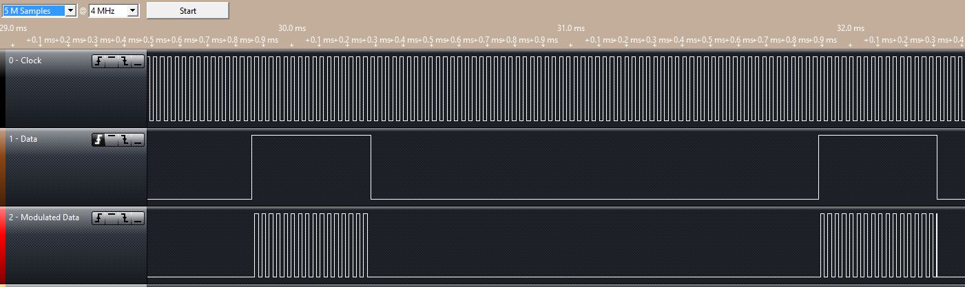
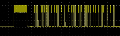
Connecting the logic analyser to the circuit will allow the examination of the three signals, namely, the digital signal required (centre trace), the clock (upper trace) and the modulated output (lower trace):
Modulated IR Signal
The solid white blocks in the clock and modulated traces show a high density of signals. Zooming in on the right hand side of the capture shows the following:
Modulated IR Signal Zoom View
As you can see, the modulated output is composed of a series of 38.4KHz clock pulses which are only generated when the digital signal should be high (logic 1). The remainder of the time the trace shows no output.
The final test is to see if this will trigger the camera, and yes, it still does.
September 7th, 2013 • Electronics, STM8 • Comments Off on Nikon D70 Infra-red Control
A few weeks ago I started to investigate infra-red transmitters with the intention of looking at implementing a remote control for my DSLR. The first post established the fundamentals by creating a low power transmitter and a receiver. This post takes this one step further and attempts to trigger the Nikon D70 DSLR under the control of a microcontroller.
Background
The Nikon D70 uses the ML-L3 infra-red remote control to trigger the camera. I chose this experiment as a first step to a more advanced remote control for my camera. The experiment builds upon the previous work with the STM8S and infra-red signals to trigger the DSLR.
The remote sequence required to trigger the Nikon D70 has been investigated before. I found the post by Michelle Bighignoli to be the most helpful for this particular exercise.
According to Michelle’s web site, the sequence of pulses required to trigger the camera is as follows:
High pulse for 2000uS
Low for 27830uS
High for 400uS
Low for 1580us
High for 400uS
Low for 3580uS
High for 400uS
The pulse is also modulated at a frequency of 38.4KHz.
Hardware
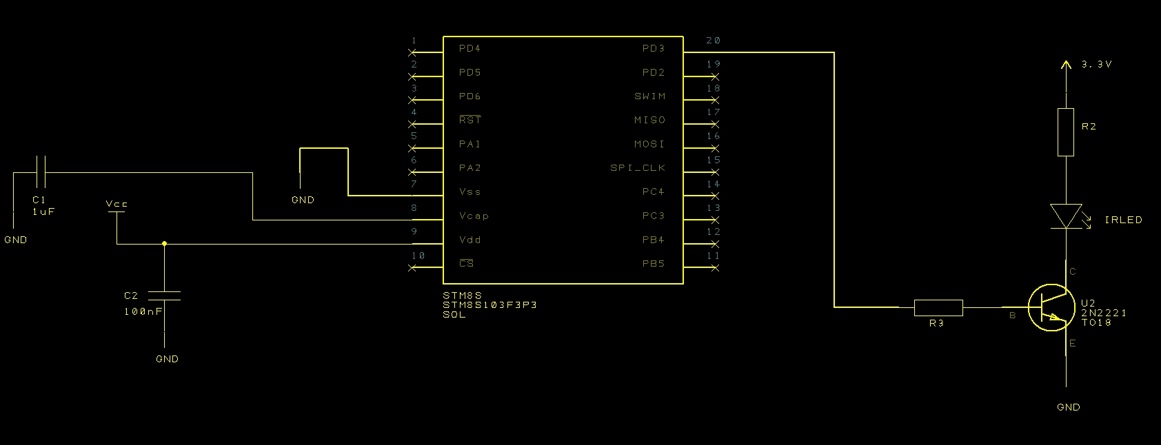
The hardware setup is going to be relatively simple. A basic STM8S circuit is connected to the IR Transmitter circuit using port D3 on the STM8S:
Nikon Infra-red Control Circuit
You can find out more information about both of these circuits by having a look at the following posts:
All that needs to be done is to put this together on breadboard and setup the STM8S ready for programming.
Software
The initial version of the software will simply emit the infra-red pulse sequence as soon as it powers up as I am only looking at a proof of concept at this stage. We will not consider the topic of modulation at this stage.
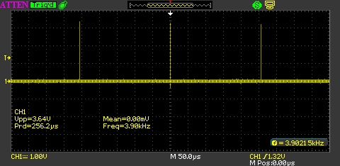
Looking at the pulse sequence, the application will need to be able to generate infra-red pulses with control down to the micro-second level. The pulse widths are reasonably large, the smallest is 400uS. Taking this into consideration, the default clock speed of 2MHz will be used for the initial version of the application.
The most obvious way of controlling the pulse widths is to use one of the built in system timers. The most obvious choice is to use Timer 2 as we are going to be using the default clock speed and only require an accuracy of a micro-second or so. This will give a count in the range 0-65535 implying that the maximum pulse width will be 65,535uS assuming we use a prescalar of 2 to divide down the clock frequency used by Timer 2 to 1MHz.
The timers use two eight bit values to control the counting. This will require that the 16-bit values we have for the pulse durations will need to be broken down into two parts either before the sequence starts or as the sequence is being generated (i.e. in the timer Interrupt Service Routine (ISR)). The method chosen here is to perform this operation before the first pulse is generated. This will allow for a quicker ISR.
Design decisions over, let’s start to look at the code.
Pulse and Timer Data
The data for the timers will be broken down into the high and low byte values for the pulse duration. Along with this we will need to store the pulse type, namely high or low.
The pulse data is stored as a sequence of on/off values along with a duration in microseconds:
This makes the pulse sequence more readable for the programmer. This data needs to be stored as a sequence of 8-bit values representing the high and low bytes of the pulse durations to speed up the ISR.
//
// Data ready for the pulse timer ISR's to use.
//
unsigned char *_counterHighBytes = NULL;
unsigned char *_counterLowBytes = NULL;
unsigned char *_outputValue = NULL;
int _numberOfPulses = 0;
int _currentPulse = 0;
And to encode the data we need a small helper method:
//--------------------------------------------------------------------------------
//
// Prepare the data for the timer ISRs.
//
void PrepareCounterData(unsigned int *pulseDuration, unsigned char *pulseValue, unsigned int numberOfPulses)
{
_numberOfPulses = numberOfPulses;
if (_counterHighBytes != NULL)
{
free(_counterHighBytes);
free(_counterLowBytes);
free(_outputValue);
}
_counterHighBytes = (unsigned char *) malloc(numberOfPulses);
_counterLowBytes = (unsigned char *) malloc(numberOfPulses);
_outputValue = (unsigned char *) malloc(numberOfPulses);
for (int index = 0; index < numberOfPulses; index++)
{
_counterLowBytes[index] = (unsigned char) (pulseDuration[index] & 0xff);
_counterHighBytes[index] = (unsigned char) (((pulseDuration[index] & 0xff00) >> 8) & 0xff);
_outputValue[index] = pulseValue[index];
}
_currentPulse = 0;
}
Now we have a method of converting the pulses into a format ready for the Timer and the ISR we need to setup the Timer and implement the ISR.
Timer Setup and ISR
Setup is simple as we just need to load the timer values for the first pulse, load the prescalar and enable the interrupts:
//--------------------------------------------------------------------------------
//
// Setup Timer 2 ready to process the pulse data.
//
void SetupTimer2()
{
TIM2_ARRH = _counterHighBytes[0];
TIM2_ARRL = _counterLowBytes[0];
TIM2_PSCR = _prescalar;
TIM2_IER_UIE = 1; // Enable the update interrupts.
}
The ISR is relatively simple, we need to work out if there is any more pulse data to process. If there is then we load the new data into the counter, set the pulse output and exit the ISR. If there is no more data then we simply set the pulse output and disable the timer.
//--------------------------------------------------------------------------------
//
// Timer 2 Overflow handler.
//
#pragma vector = TIM2_OVR_UIF_vector
__interrupt void TIM2_UPD_OVF_IRQHandler(void)
{
_currentPulse++;
if (_currentPulse == _numberOfPulses)
{
//
// We have processed the pulse data so stop now.
//
PD_ODR_ODR3 = 0;
TIM2_CR1_CEN = 0;
}
else
{
TIM2_ARRH = _counterHighBytes[_currentPulse];
TIM2_ARRL = _counterLowBytes[_currentPulse];
PD_ODR_ODR3 = _outputValue[_currentPulse];
TIM2_CR1_URS = 1;
TIM2_EGR_UG = 1;
}
TIM2_SR1_UIF = 0; // Reset the interrupt otherwise it will fire again straight away.
}
Output Port
As noted, the application is using Port D3 to output the signal. A small method is required to setup the port accordingly:
//--------------------------------------------------------------------------------
//
// Now set up the output ports.
//
// PD3 - IR Pulse signal.
//
void SetupOutputPorts()
{
PD_ODR = 0; // All pins are turned off.
//
// PD4 is the output for the IR control.
//
PD_DDR_DDR3 = 1;
PD_CR1_C13 = 1;
PD_CR2_C23 = 1;
}
Main program Loop
The main program loop merely sets the stage by initialising the data, output port and timer before wiating for wny interrupts:
//--------------------------------------------------------------------------------
//
// Main program loop.
//
void main()
{
unsigned int pulseLength[] = { 2000U, 27830U, 400U, 1580U, 400U, 3580U, 400U };
unsigned char onOrOff[] =    {   1,      0,     1,     0,    1,     0,    1 };
PrepareCounterData(pulseLength, onOrOff, 7);
__disable_interrupt();
SetupTimer2();
SetupOutputPorts();
__enable_interrupt();
PD_ODR_ODR3 = _outputValue[0];
//
// Now we have everything ready we need to force the Timer 2 counters to
// reload and enable Timer 2.
//
TIM2_CR1_URS = 1;
TIM2_EGR_UG = 1;
TIM2_CR1_CEN = 1;
while (1)
{
__wait_for_interrupt();
}
}
Conclusion
Putting this all together and wiring up the oscilloscope we find the following generated when the circuit is turned on:
Output From Nikon Infra-red Control Circuit
Examination of the timings of the pulses reveals that the pulse widths match those in the original specification above. The small spike at the start of the pulse sequence only appears when the circuit is first turned on.
At the moment we are only generating the raw pulses, we have not started to modulate the signal using the 38.4KHz carrier. This is left for a future experiment or indeed as a exercise for the reader.
One thing I could not resist was trying this with the Nikon camera, even though the specification stated that a 38.4KHz carrier was required. Running the code with the camera set to manual mode resulted in the camera being triggered.
A while ago I wrote a small library for the RN-42 Bluetooth module. This small module acted as a serial port when connected to the Netduino. Times have moved on with Bluetooth 4.0 being available on the iPhone I thought I would take another look at Bluetooth.
Bluetooth Module
The Bluetooth module we will be using is the RedBear Bluetooth Mini. This little module is a Bluetooth 4.0 Low Energy (BLE) module. In it’s simplest form it offers the ability to act as a serial port for your project. This is how we will be using this module for this project.
Bluetooth Device
To test this a BLE compatible device is required. Enter the iPhone 5 and the BLE Arduino application which RedBear have thoughtfully provided. The application may be written for Arduino but it is sending simple serial commands to the Arduino. Let’s see what it is doing and if we can use this application.
Serial Port Settings
First job is to figure out the serial port settings. Scanning the source code for the Arduino I came across the following line in the setup method:
BleFirmata.begin(57600);
My guess is that this is setting up the Arduino serial port to run at 57,600 baud using standard data bits, parity and top bit settings. Time to break out the logic analyser.
Connections between the Netduino and the RedBear module is simple:
Netduino Pin
Redbear BLE Module Pin
D0 (Rx)
Tx
D1 (Tx)
Rx
3.3V
Vin
GND
GND
Additionally, the logic analyser is connected to the Rx and Tx pins of the Netduino. An Async Serial analyser was added to the two pins through the Saleae software. This analyser has an Autobaud feature. Turn this on just in case we get the baud rate incorrect.
Next step is to install the BLE Arduino application on the iPhone 5. Start the application:
ReadBear BLE Software Opening Screen
Press the Click button to connect to the ReadBear module.
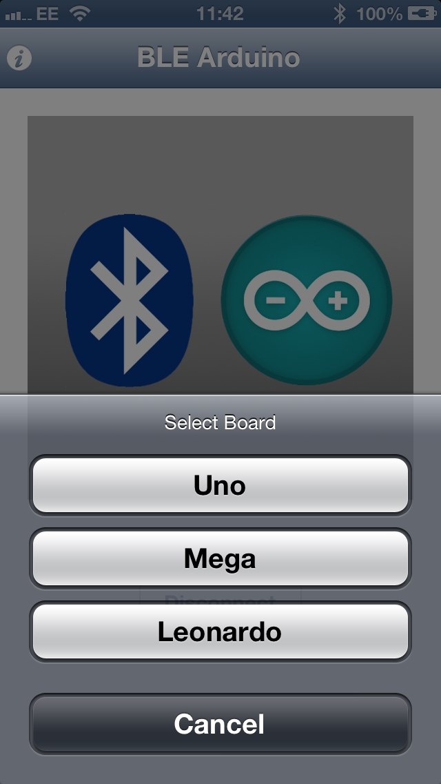
Select Arduino Board
Select the Arduino to connect to. The Arduino Uno has a similar pin out so select the Uno option.
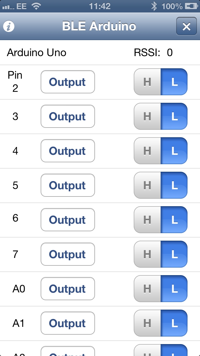
Change a Pin Output Using BLE Software
So far there has been no output on the logic analyser. Change the state of an output pin (pressing H or L). This generates serial data:
Serial Data On the Logic Analyser
A quick check in the Async Serial analysers properties shows that the data logic analyser thinks that the data is being sent at 60,000 baud, pretty close to the 57,600 which was found in the code earlier.
Netduino Code
The next step is to try to connect some code on the Netduino to the iPhone application. The simplest application we can use simply captures the incoming data on the serial port and displays the bytes received in the debug window of Visual Studio. The following should do the trick:
public class Program
{
    const int BUFFER_SIZE = 1024;

    public static void Main()
    {
        SerialPort sp = new SerialPort("COM1", 57600, Parity.None, 8, StopBits.One);
        sp.DataReceived += sp_DataReceived;
        sp.Open();
        Thread.Sleep(Timeout.Infinite);
    }

    static void sp_DataReceived(object sender, SerialDataReceivedEventArgs e)
    {
        string str;
        str = "";
        if (e.EventType == SerialData.Chars)
        {
            int amount;
            byte[] buffer;

            buffer = new byte[BUFFER_SIZE];
            amount = ((SerialPort) sender).Read(buffer, 0, BUFFER_SIZE);
            if (amount > 0)
            {
                for (int index = 0; index < amount; index++)
                {
                    str += buffer[index].ToString();
                    str += " ";
                }
                Debug.Print("Data: " + str);
            }
        }
    }
}
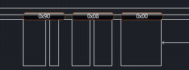
Deploying the above code to my Netduino Plus 2 and running the application gives the following output:
Pressing the H at the side of Pin 2 in the application generates the sequence 144 4 0. Following this up by pressing the H at the side of Pin 3 results in the sequence 144 12 0. Checking the Arduino code shows that the digital commands are prefixed by 0x90, i.e. 144.
The iPhone Application
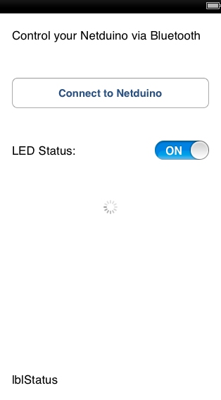
Now that we know the iPhone and the Netduino can communicate (at least from the phone to the Netduino) let’s have a look at creating our own iPhone application. The simplest application would entail toggling a digital pin, so let’s do that. We’ll turn an LED on and off.
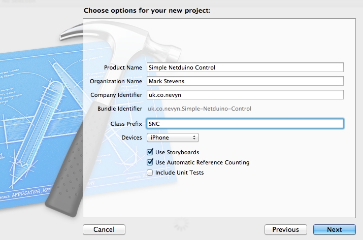
Starting XCode we will create a new project (Single View Application) for the iPhone and set the application be targeted at the iPhone only and to use Automatic Reference Counting (ARC):
New iPhone Project Options
Next we need to add the CoreBluetooth.Framework references to the application. So scroll down the frameworks and click on the + button under the Linked Frameworks section. Type bluetooth in order to search the installed frameworks.
Next, we need to add the RedBear BLE framework. I downloaded this and put it in my stored libraries. This was then added by right clicking on the Frameworks folder of the project, selecting Add Files to… and then browsing to the folder which contained the files.
Next we head over to the Storyboard and add a few controls to our interface:
iPhone Application in XCode
Control
Description
btnConnectToNetduino
Button to connect/disconnect to/from the Netduino.
lblStatus
Label to indicate the status of the application.
lblLEDStatus
Label containing the text LED Status
swLED
Switch which is used to turn the LED on/off.
aiBusy
Indicator which shows when the application is trying to detect the Bluetooth module.
First thing to do is to connect the controls to the code in the header file for the view controller:
These definitions create the Bluetooth object and he variables required for state control.
Supporting Methods
The Connected and Disconnected methods change the interface and state variables when we have successfully connected or disconnected to/from the Bluetooth module:
//
//  Set up the interface to show that the Bluetooth module is connected
//
- (void) Connected
{
    [lblStatusMessage setText:@"Connected"];
    lblLEDStatus.hidden = false;
    swLED.hidden = false;
    [btnConnectToNetduino setTitle:@"Disconnect from Netduino" forState:UIControlStateNormal];
    btnConnectToNetduino.enabled = true;
    [self.aiBusy stopAnimating];
    mode = MODE_CONNECTED;
}

//
//  Set up the interface to show that the Bluetooth module is disconnected
//
- (void) Disconnected
{
    [lblStatusMessage setText:@"Disconnected"];
    lblLEDStatus.hidden = true;
    swLED.hidden = true;
    [btnConnectToNetduino setTitle:@"Connect to Netduino" forState:UIControlStateNormal];
    btnConnectToNetduino.enabled = true;
    [self.aiBusy stopAnimating];
    mode = MODE_DISCONNECTED;
}
Standard Methods (viewDidLoad and didReceiveMemoryWarning)
These methods are generated by default when the application is first created. For viewDidLoad we will set up the application for initial use. We will not be modifying the didReceiveMemoryWarning method in this application.
//
//  Setup the view.
//
- (void) viewDidLoad
{
    [super viewDidLoad];
    //
    //  Setup the display.
    //
    lblLEDStatus.hidden = true;
    [swLED setOn:NO];
    swLED.hidden = true;
    [lblStatusMessage setText:@"Ready"];
    self.aiBusy.hidesWhenStopped = true;
    //
    //  Create the Bluetooth objects.
    //
    ble = [[BLE alloc] init];
    [ble controlSetup:1];
    ble.delegate = self;
    //
    //  Setp the simple properties.
    //
    mode = MODE_DISCONNECTED;
}

//
//  Process the memory warning event.
//
- (void) didReceiveMemoryWarning
{
    [super didReceiveMemoryWarning];
}
The main point to note in the viewDidLoad method is that the Bluetooth object is initialised.
Button Press Event
The btnConnect_TouchUpInside event initiates the connection/disconnection of the application to/from the Bluetooth module.
//
//  User has pressed the Connect button so try to connect/disconnect from the Netduino.
//
- (IBAction) btnConnect_TouchUpInside:(UIButton *) sender
{
    if (ble.activePeripheral)
    {
        if (ble.activePeripheral.isConnected)
        {
            [[ble CM] cancelPeripheralConnection:[ble activePeripheral]];
        }
    }
    ble.peripherals = nil;
    switch (mode)
    {
        case MODE_DISCONNECTED:
            [lblStatusMessage setText:@"Connecting..."];
            [NSTimer scheduledTimerWithTimeInterval:(float) TIMEOUT_BUSY_CONNECTING target:self selector:@selector(connectionTimer:) userInfo:nil repeats:NO];
            [ble findBLEPeripherals:TIMEOUT_BLE_TIMEOUT];
            [self.aiBusy startAnimating];
            mode = MODE_CONNECTING;
            break;
        case MODE_CONNECTED:
            [lblStatusMessage setText:@"Disconnecting..."];
            [self.aiBusy startAnimating];
            mode = MODE_DISCONNECTING;
            break;
        default:
            break;
    }
    btnConnectToNetduino.enabled = false;
}
Timer
The btnConnect_TouchUpInside event starts a timer when it is trying to connect to a Bluetooth module. This timer prevents the application from locking when searching for a Bluetooth module which does not exist. The timer callback stops the search process after 3 seconds:
//
//  The timer started by the Connect button has triggered.  See if we have any
//  Bluetooth modules nearby.  If we have then connect to the first one in the
//  list.
//
-(void) connectionTimer:(NSTimer *) timer
{
    if (ble.peripherals.count > 0)
    {
        [ble connectPeripheral:[ble.peripherals objectAtIndex:0]];
    }
    else
    {
        [lblStatusMessage setText:@"Cannot find Netduino"];
        mode = MODE_DISCONNECTED;
    }
    [self.aiBusy stopAnimating];
}
Switching the LED on/off
The application assumes only one LED is connected to the Netduino. The data packet sent to the Netduino therefore contains a 1 or 0 to indicate the status of the LED:
//
//  User has changed the value of the LED.
//
- (IBAction) swLED_Changed:(UISwitch *) sender
{
    UInt8 buffer[1];
    buffer[0] = sender.isOn == YES ? 1 : 0;
    NSData *data = [[NSData alloc] initWithBytes:buffer length:1];
    [ble write:data];
}
Bluetooth Module Events
The final two events are generated by the Bluetooth library. These are fired when the module connects/disconnects to/from the module:
//
//  Connected to a Bluetooth module successfully.
//
-(void) bleDidConnect
{
    [self Connected];
}

//
//  Application has disconnected from a Bluetooth module.
//
- (void) bleDidDisconnect
{
    [self Disconnected];
}

//
//  RSSI has been updated.
//
- (void) bleDidDisconnect:(NSNumber *) rssi
{
}
Netduino Application
The final task is to modify the Netduino Application to process the data. An OutputPort is added to the application and this is connected to a digital IO pin. This pin is then turned on/off when serial data is received from the Bluetooth module:
public class Program
{
    const int BUFFER_SIZE = 1024;
    private static OutputPort led = new OutputPort(Pins.GPIO_PIN_D8, false);

    public static void Main()
    {
        SerialPort sp = new SerialPort("COM1", 57600, Parity.None, 8, StopBits.One);
        sp.DataReceived += sp_DataReceived;
        sp.Open();
        Thread.Sleep(Timeout.Infinite);
    }

    static void sp_DataReceived(object sender, SerialDataReceivedEventArgs e)
    {
        string str;
        str = "";
        if (e.EventType == SerialData.Chars)
        {
            int amount;
            byte[] buffer;

            buffer = new byte[BUFFER_SIZE];
            amount = ((SerialPort) sender).Read(buffer, 0, BUFFER_SIZE);
            if (amount > 0)
            {
                for (int index = 0; index < amount; index++)
                {
                    str += buffer[index].ToString();
                    str += "";
                }
                if (buffer[0] == 1)
                {
                    led.Write(true);
                }
                else
                {
                    led.Write(false);
                }
                Debug.Print("Data: " + str);
            }
        }
    }
}
Does it Work?
Well of course it does and here’s the video to prove it:
First we connect to the module. Once connected we can start to turn the LED on and off using the iPhone.
Conclusion
The library provided by RedBear is a great starting point for using the iPhone to communicate with a BLE module. It is simple and easy to use for this type of application. This whole experiment only took a few hours to put together an execute.
August 18th, 2013 • Electronics • Comments Off on Infra-red Transmitter and Receiver
In this post we will use Mr Maxwell’s new fangled electrons to generate invisible light and transmit a signal through the luminiferous aether.
Or to put it another way, I’m learning how to use IR remote controls in microcontroller circuits. The problem with using infra-red LEDs is that you cannot really see if they are on or off. You can see if a signal is applied to the LED but this does not mean it’s generating an infra-red signal. Let’s admit it, we’ve all burnt out an LED or two in our time. So in this post I’m going to put together a couple of circuits to generate and detect infra-red signals.
Detecting IR Signals
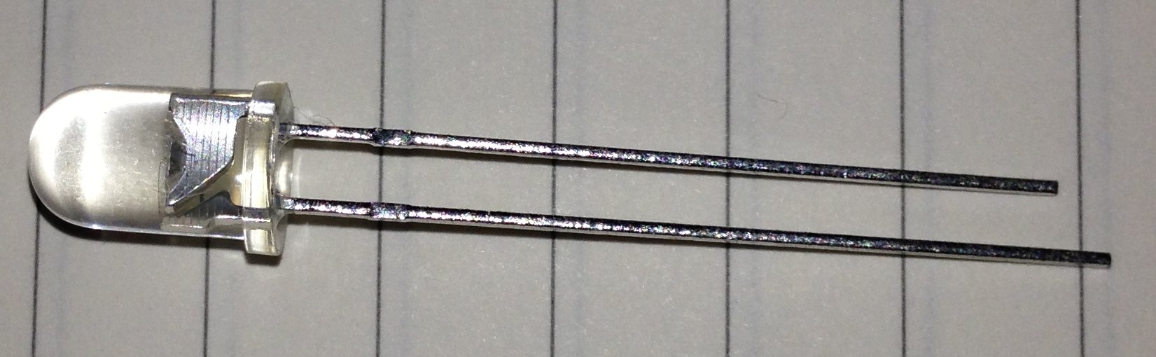
For this circuit I am going to be using the L-7113P3C phototransistor. This component looks like an LED but is in fact a transistor:
Photo Transistor
The phototransistor has two conventional connections which allow the collector and emitter to be connected to the electrical circuit but the third connector (the base) has been made sensitive to infra-red light and then exposed via a lens. The transistor becomes conductive when infra-red light hits the photosensitive base of the transistor.
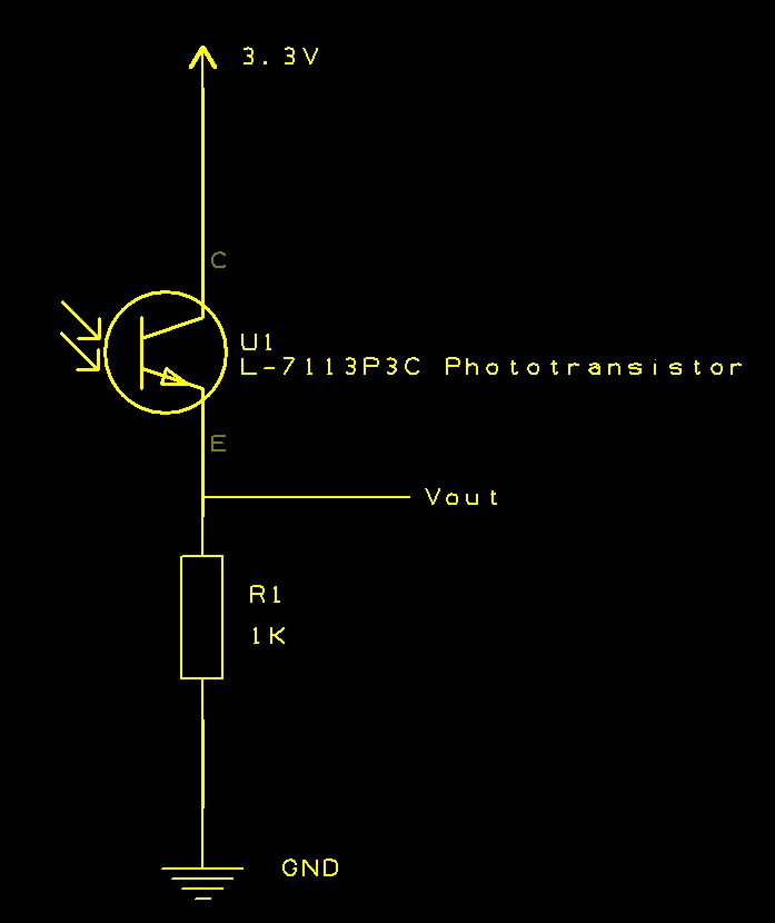
The schematic for the basic detector circuit is as follows:
IR Receiver Schematic
Should be simple enough. Out comes the breadboard, oscilloscope and a couple of remote controls I have to hand.
Simple IR Receiver
Connecting the Vout to the oscilloscope and pointing a WD TV remote control at the phototransistor I saw the following trace:
WD TV Remote Signal
So, it looks like the detector circuit is detecting the infra-red signal from these remote controls.
Infra-red Transmitter
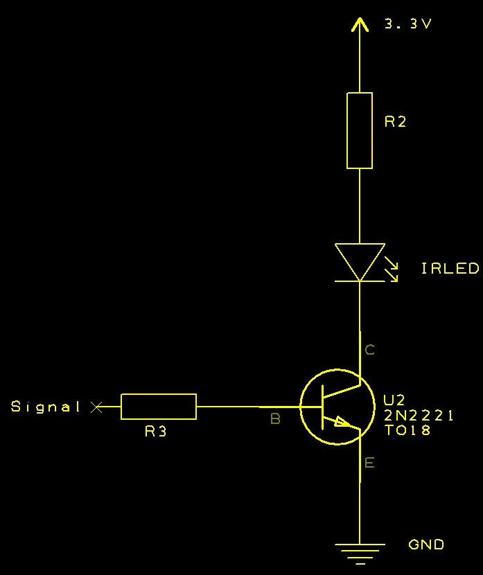
The transmitter circuit is simply an infra-red LED with visible LED replaced by an infra-red LED. For this circuit I used the TSUS5400 as this is matched with the L-7113P3C phototransistor I used in the detector circuit. Dropping this into a simple LED/transistor circuit gives the following schematic:
IR Transmitter Schematic
R2 was selected to allow 20mA of current through the infra-red LED (IRLED). The resistor on the base of the transistor should allow the transistor to become saturated. Dropping this on breadboard gives a circuit which looks like this:
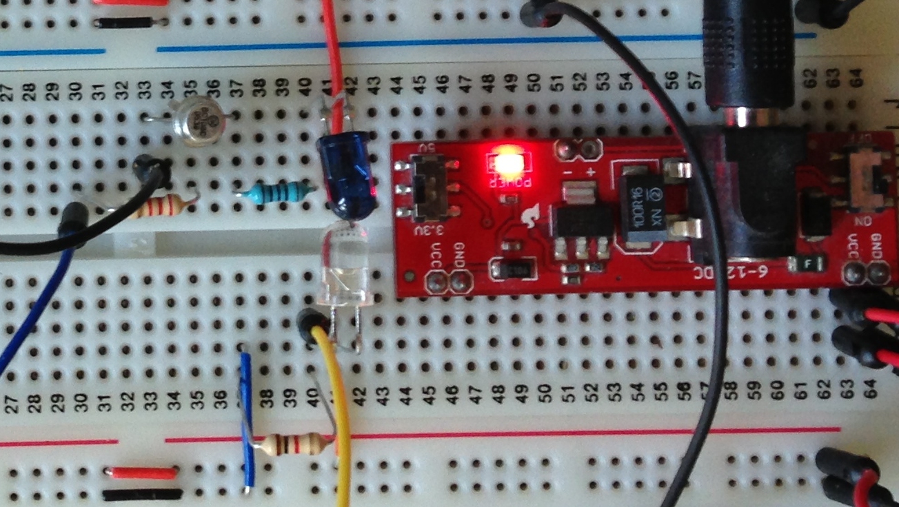
IR Transmitter and Receiver
The top part of the breadboard contains the transmitter circuit (Blue LED) and the lower part of the breadboard contains the receiver.
Testing
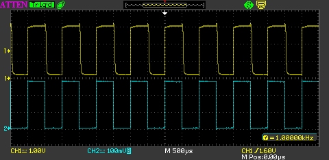
To test the circuit a 1KHz signal generator was connected to the base of the transmitter circuit. Channel 1 (yellow) of the oscilloscope is connected to Vout of the receiver with channel 2 (blue) connected to the signal generator. Turning on the signal generator produced the following output on the oscilloscope:
1 KHz Signal
Looking good. The signals show a good match.
Conclusion
The main aim of this exercise was to create an infra-red receiver circuit which can be used to verify that an equivalent transmitter circuit is working. The receiver circuit gives a value for Vout of 3.12V. This is an acceptable value for logic 1 for the microcontrollers which I am using. Their nominal input value for logic 1 is the supply voltage +/- 0.3V.
The transmitter circuit should allow the use of the same microcontroller to generate a signal which can be used to control a device such as a TV etc.
July 21st, 2013 • Electronics • Comments Off on Designspark Feature Tutorial – ModelSource
I have been a great fan of Designspark for a while. Many hobbyists swear by Eagle. Personally, I find the interface counter intuitive. Designspark on the other hand, feels like a Windows application.
Shortly after Designspark version 5 was released, I noticed a new toolbar in the bottom lefthand corner of the interface. This toolbar was labelled ModelSource. So like all good software users I went to the manual to find out more <COUGH>, OK, I simply started to play with the feature and here’s a summary of what I found.
What Is ModelSource?
ModelSource is Designspark’s free on-line database of component models. The library is by no means complete but it does provide a large on-line library of components to choose from. At the time of writing, there are over 80,000 components in the library. The library is linked to RS Components but this is to be expected as Deisgnspark seems to have been originated/sponsored by RS.
Interestingly, the library is also compatible with other software packages.
Let’s Use It
The quickest way to become familiar with a software feature is to use it. So let’s add a component I’ve never used before to a schematic. For this example we will use the 74HC164.
We start by opening the ModelSource toolbar. This is can be found in the bottom left corner of the application window and looks like this:
ModelSource Toolbar Collapsed
If you cannot see the ModelSource toolbar then you can check if it is visible. by looking at the View menu. Alternatively, you can use the hotkey Ctrl-M to make it visible.
The first time you make ModelSource visible you will have to log in using your Designspark credentials. Once logged in, you can access ModelSource.
Clicking on ModelSource opens the toolbar. This can appear as required or you can permanently pin this in the open state to the interface. When first opened ModelSource will be ready to accept search requests from the user:
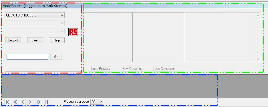
ModelSource
There are really three distinct areas to the interface:
Search Parameters (Red Rectangle)
Component Detail (Green Rectangle)
Component List (Blue Rectangle)
Search Parameters
The Search Parameters section of the interface is in the upper left part of ModelSource and it allows you to search ModelSource by component family or for a specific component using the RS part number.
Component Detail
Component Detail sows the schematic and PCB trace for a selected component along with summary information. This can be found to the right of the Search Parameters. This section also allows you to go to the component data sheet and add the component to your library.
Component List
Component List contains a grid of components which match your search criteria.
Searching For A Component
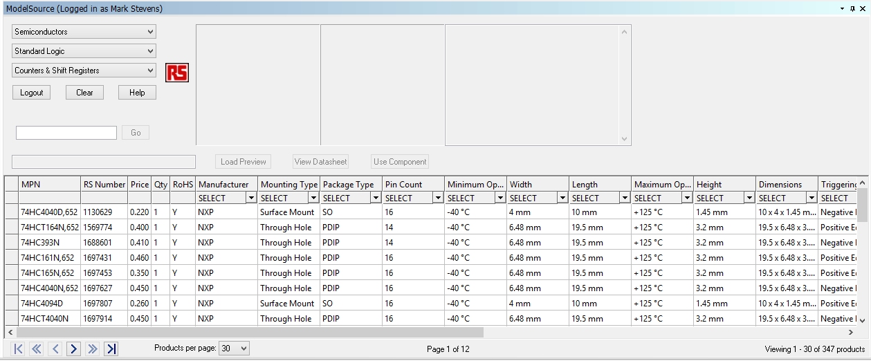
The component we are searching for is the 74HC164. This is a 8-bit shift register from the 74HC family of components.
The search process requires the user to select from a list of possible family groups/characteristics slowly narrowing the search down to a group of components which you can then browse through. So for the 74HC164 we start by selecting Semiconductors from the first drop down list. The system will then consult the ModelSource database and construct sensible options for the second drop down list which will then be populated.
This component is a shift register and so it probably best fits into the Standard Logic family of components. So we select this in the second drop down list. Again, Designspark will select a new set of options for the third drop down list.
The final list now contains the family of components we are looking for, namely Counters & Shift Registers. Selecting this option now allows Designspark to populate the component list from the ModelSource database and we are presented with the following:
Semiconductor search for Counters and Shift Registers
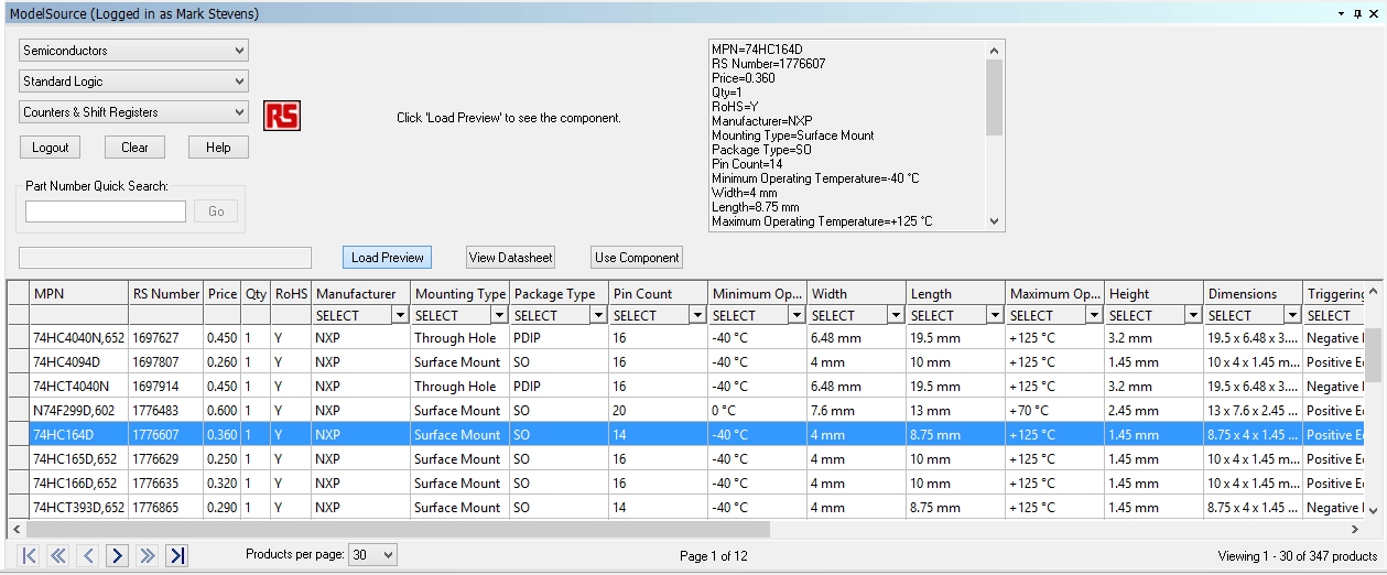
As you can see, you can use the drop down lists above each column to filter the information presented in the component list should you require to refine the results further. A quick look down the list and we can see our component, the 74HC164. So let’s select the 74HC164D component in the grid:
74HC164D Ready to load preview
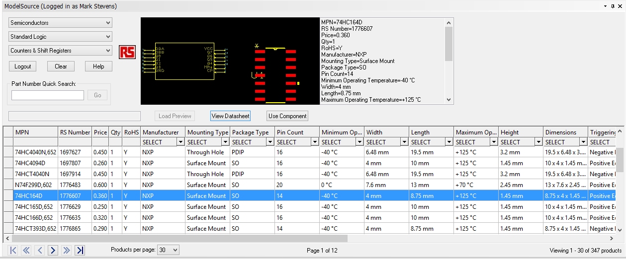
And now press the Load Preview button. Designspark will then load the component preview information from ModelSource:
74HC164 Preview Complete
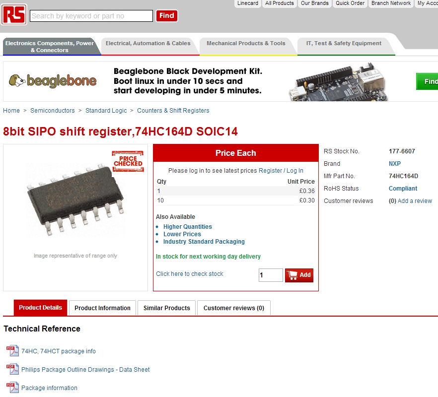
At this point we have two options, we can use this component immediately and add it to the schematic or we can view the datasheet. Clicking on View Datasheet takes you to the RS web site and presents the page for the component. Here you can add the component to your basket or scroll down the page to the datasheet links:
74HC164 Web page
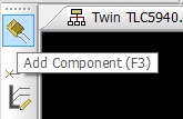
By selecting Use Component you make the component available through the library installed on your computer. Whilst in the schematic editor press the Add Component Button
Add Component button
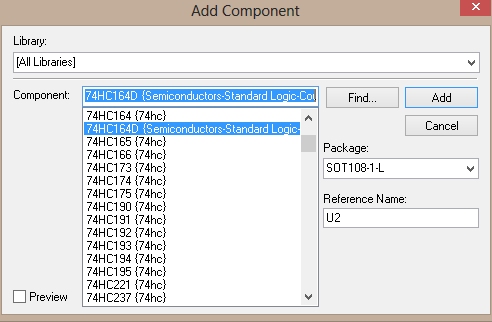
and type in the component name into the Component text box in the Add Component dialog:
Add 74HC164 component to schematic
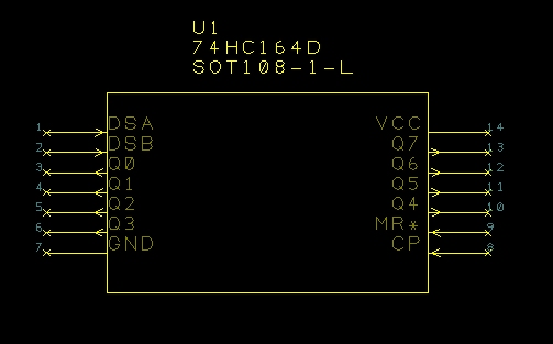
You can now add the component to the schematic:
74HC164 on schematic
Searching for a Component by Part Number
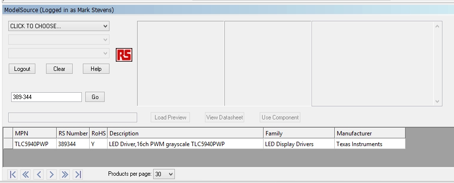
It is sometimes simpler to use the RS Components web site to locate the part you are looking for and then use the Part Number Search option to locate the component. For example, consider the TLC5940 shift register. It is difficult to work out from the list of search options in the drop down list boxes exactly what you should be selecting.
In comparison, go to the RS Components web site and enter TLC5940 in the search text box on the home page and press the Find button. You will be taken to a page with three components, all variations on the TLC5940 16 channel PWM driver. Now make a note of the RS part number (I have the 389-344 variation of this component).
So go back to ModelSource and press the Clear button. Now enter the component part number into the Part Number Quick Search text box and press the Go button:
TLC5940 search for part number
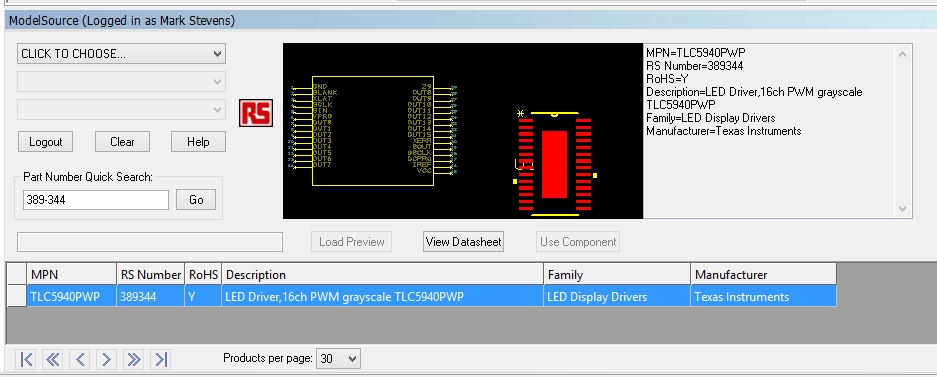
Selecting the part and pressing Load Preview shows the part information:
TLC5940 ModelSource Preview
Conclusion
ModelSource is not a complete database but with 80,000 components it offers a very good chance of finding the component you need for the circuit you are building. I have used this on several occasions to find models for components which do not exist in the standard installation.
There is no question that this could be improved. For instance, why can you not search by component name as you can in the web interface?
Overall this is a good product feature and whilst it is linked through to the RS Components web site it does not necessarily mean you have to order from there.
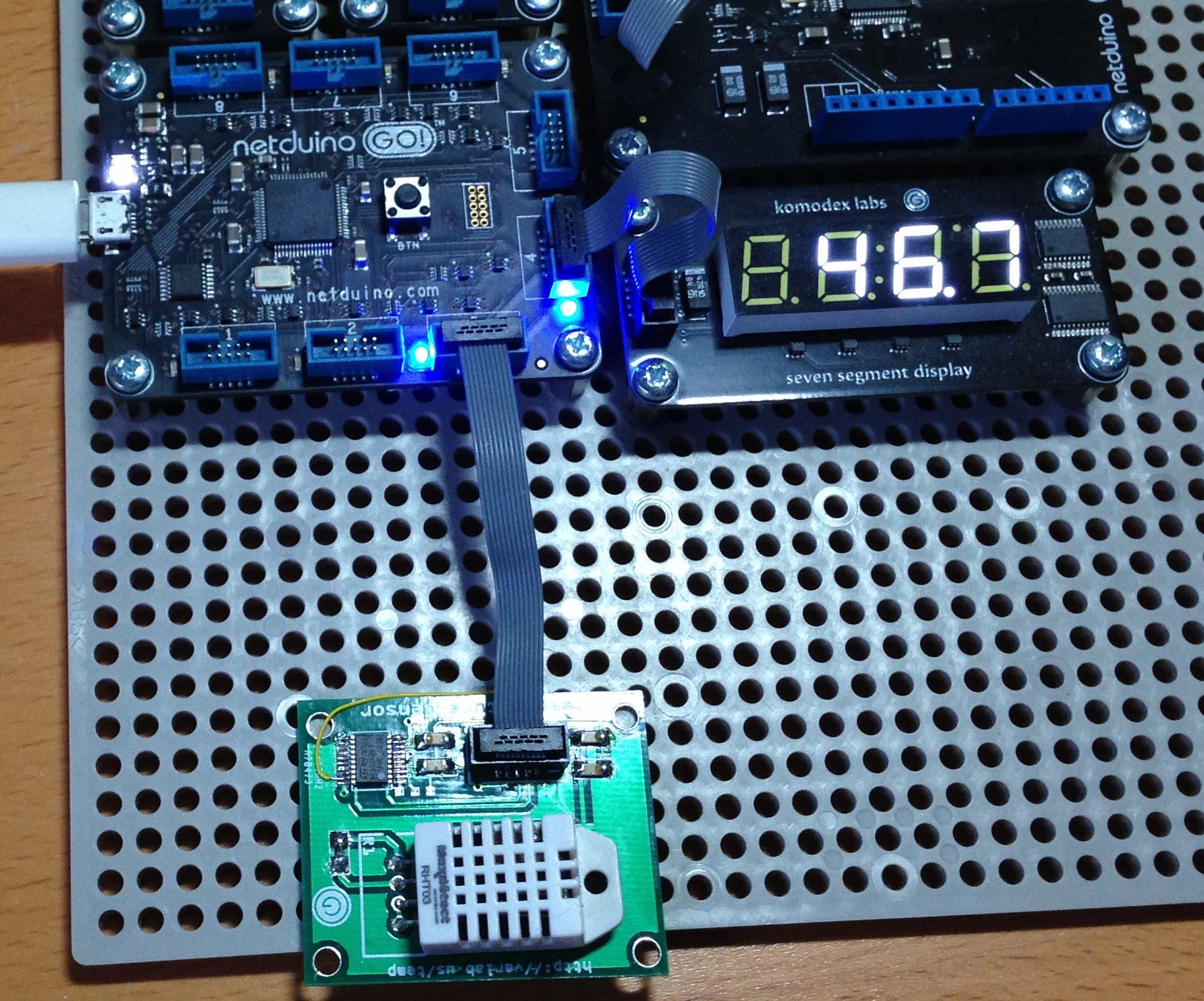
A while ago (forgive the pun), Arron Chapman and I started to collaborate on building a temperature and humidity sensor based upon the DHT22 sensor. One of the original posts discussing the module can be found here in the Netduino forums. From the very start we agreed that both the hardware and software would be open source. This post will discuss the basic hardware requirements and the software required to create a Temperature and Humidity Module for the Netduino GO!.
This post has a software bias given the relatively simple nature of the hardware being developed. Here is a flavour of what was achieved:
The design work for this module is the combined effort of Arron Chapman of Variable Labs and myself.
DHT22 Temperature and Humidity Sensor
The DHT22 is a four pin package capable of measuring temperature (+/- 0.5C) and humidity (+/- 5%). The package uses a single wire interface for communication and can be powered by 3.3-5V. The single wire protocol used is not compatible with Dallas single wire protocol.
The four pins should be connected as follows:
Pin
Connection
1
VDD (3.3-5V)
2
Data/Signal
3
Ground
4
Ground
Pin 2 (Data/Signal) should be connected to the microcontroller with a pull-up resistor to VDD.
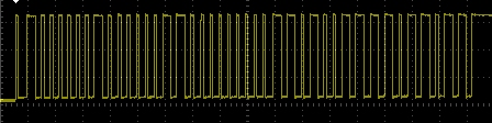
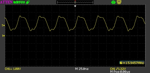
The microcontroller sends a start signal to the sensor which then responds with the data representing the temperature and humidity. The data is terminated with a check sum. The sensor can only be read at most once every 2 seconds. The trace for a full start, transmit and end signal looks like this:
The communication starts with the microcontroller sending the start signal. The microcontroller pulls the signal line low for at least 1-10ms. This ensures that the sensor can detect the microcontrollers signal. The microcontroller then pulls up the signal line and then waits for 20-40us for the sensor to respond.
Zooming in on the start packet we would see something like:
As you can see, in this case the signal line was pulled low by the microcontroller for about 6.25mS.
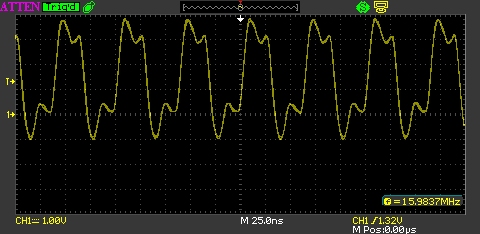
The sensor then pulls the signal line low for 80us followed by pulling up the signal line for a further 80us. At this point the sensor is ready to start to transmit the temperature and humidity data.
The data is transmitted by varying the length of time the signal pin is held high. Transmission of a single bit starts by pulling the signal line low. A 0 bit is indicated by the sensor pulling the signal line high for 26-28us. pulling the signal high for 70us indicates a 1.
The temperature and humidity data is transmitted in a 40-bit packet. The first 16 bits hold the humidity information, the next 16 bits hold the temperature information and the final 8 bits contains the checksum. The following shows the full data packet from the sensor:
Both the temperature and the humidity are represented as an integer. The actual value is obtained by converting the binary number to decimal and then dividing by 10. If the high bit of the temperature reading is 1 then the value represents a negative temperature.
The final 8 bits of the data packet contain the checksum. The checksum is the result of adding the four bytes of the temperature and humidity data.
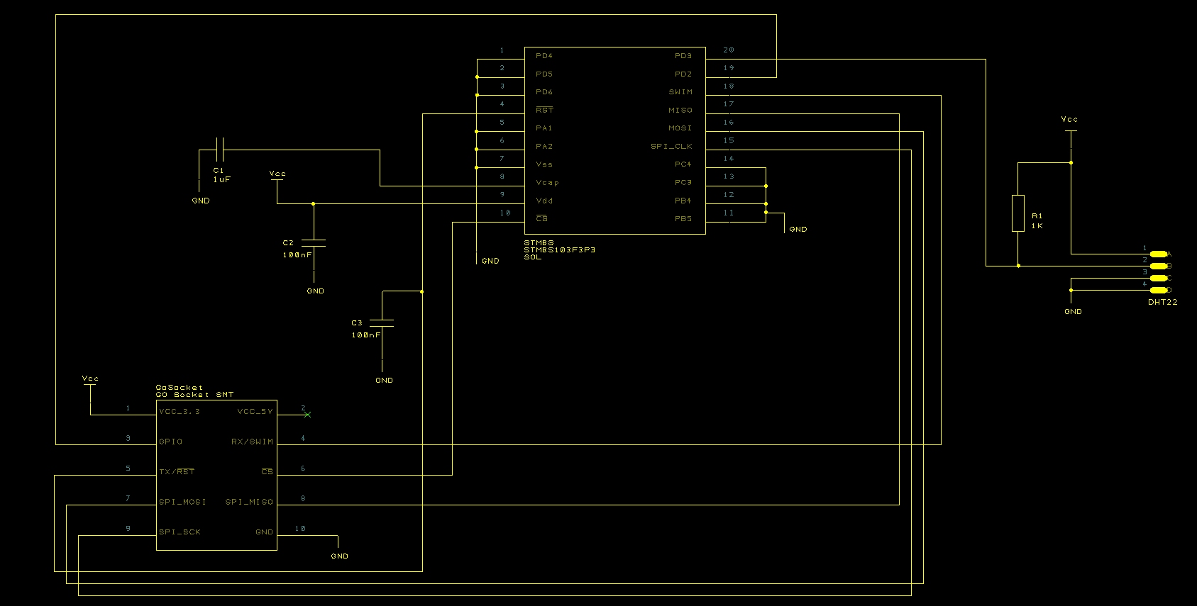
Schematic
Aside from the components required to make a basic module, the board really only required two parts, a single pull-up resistor and the DHT22 Temperature and Humidity sensor itself.
The components to the left of the diagram should be familiar if you have read the previous posts on making a module. The only additional parts can be seen to the right of the schematic.
Breadboard and PCB Prototypes
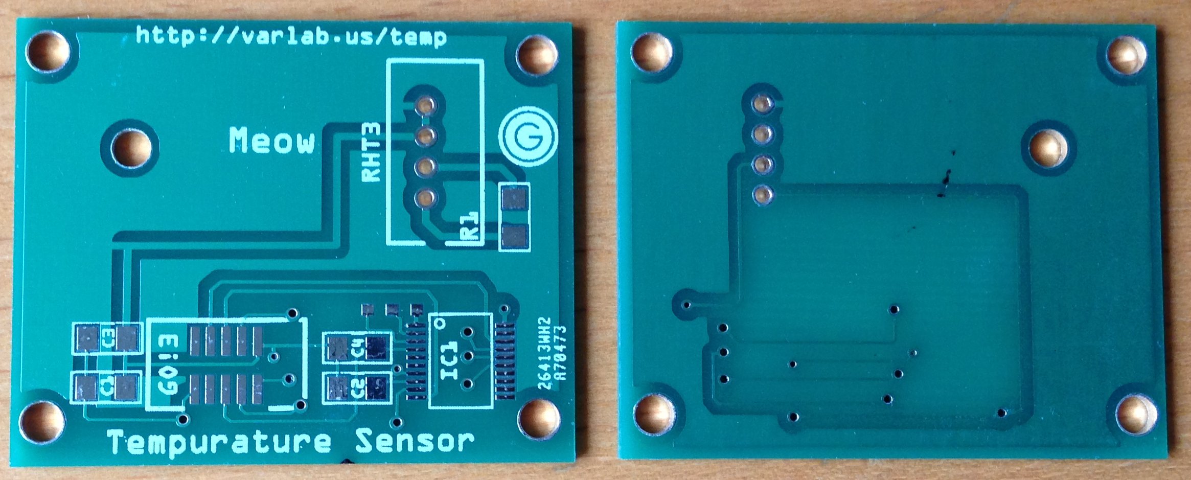
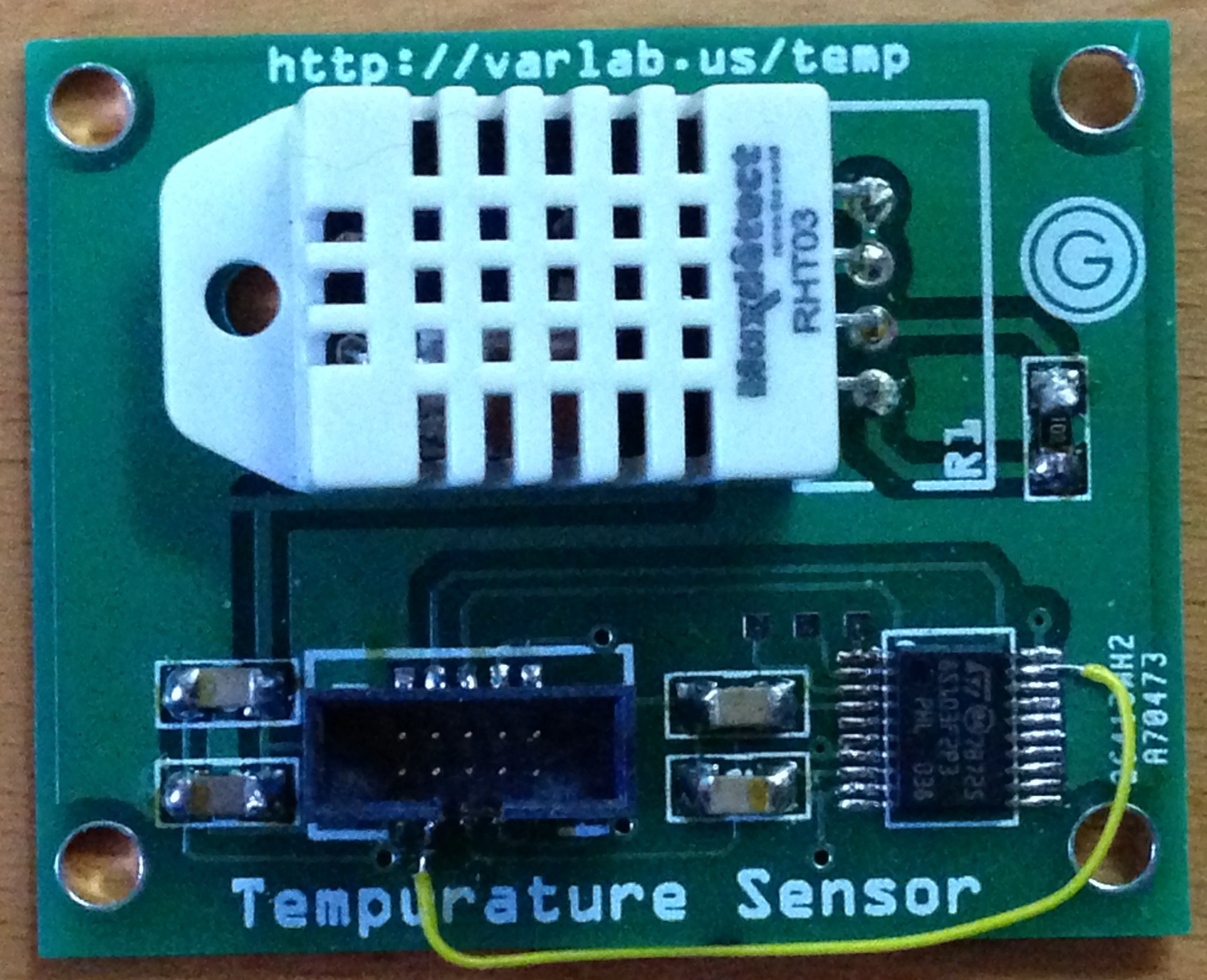
The original work for this module was completed on breadboard with an additional LM35 temperature sensor at the side of the DHT22. This second sensor was used as a reference to confirm the readings being generated by the DHT22. The simplicity of the design meant that moving to a PCB prototype was relatively simple and the iTeadStudio prototyping service made this affordable. A few weeks after ordering the prototype modules arrived:
One of the tests I do on any PCBs I have made is a connectivity test. I do this when the board is unpopulated and simply walk through the list of connections and verify that there are no problems. I also take the software I have written during prototyping on the breadboard and check that the pins on the STM8S are connected to the correct points on the PCB. It was during this test that I found that a connection had been missed off of the original schematic, namely the connection from the GO! connector and the GPIO pin which is used to signal that data is ready for the GO! to consume. A quick fix once the board had been populated.
Notice the yellow wire – this goes to show the value of prototyping even for the smallest and seemingly simplest of projects.
Software
The one wire protocol means that the microcontroller will be both a master and a slave device as will the DHT22. We also have to allow for the fact that we also have the leave a 2 second gap between readings. The ideal way to implement this is to use a finite state machine. The cycle of events is as follows:
Send the start signal and wait for 1-10ms
Enter read mode and collect data
Pause for at least 2 seconds
The state machine relies upon the timers to change the state based upon the minimum values for the time periods set by the sensor.
For the start signal, the signal line is set low and the timer started.
When the timer interrupt is triggered, the timer is turned off and reset. The signal pin is then switched from being an output pin to input with interrupts enabled. The timer is then restarted with a time period slightly larger than that required to ready all 40 bits of data from the sensor.
In the final stage, the interrupts are turned off, the data is processed and the system put to sleep (from a reading point of view) for more than 2 seconds.
In read mode, the system merely waits for interrupts to be generated by the sensor changing the state of the signal line. When an interrupt occurs, the time stamp (from the currently running timer) is read and recorded. The duration of the signal can then be calculated later (in stage three, pause mode) and the bit stream reconstructed from the timings.
Functionality
From a high level, the temperature and humidity module should provide the ability to read the current temperature and humidity (given the restrictions on the sensors delay of 2 seconds between readings). In addition, it would be desirable to allow the system to generate alarms for readings which are out of range.
As with all Netduino GO! modules, this functionality is split between the module and the module driver running on the Netduino GO!. The code on the module takes care of all the communication with the sensor. It takes this information and then responds to requests from the module driver on the Netdunio GO!.
STM8S Module
The software on the STM8S started life as the basic STM8S module software which has been used in previous posts.
The first modification needed is to add the state machine. The STM8S periodically reads the values from the sensor and store them for later retrieval by the Netduino GO! The regular nature of this update means that there is always a “current” reading available to the Netduiino GO! So the first thing we need is to setup a timer:
//--------------------------------------------------------------------------------
//
//  Setup Timer 2 to pause for 3.2 seconds following power up.
//
void SetupTimer2()
{
    TIM2_PSCR = 0x0a;       //  Prescaler = 1024
    TIM2_ARRH = 0xc3;       //  High byte of 50,000.
    TIM2_ARRL = 0x50;       //  Low byte of 50,000.
    TIM2_IER_UIE = 1;       //  Enable the update interrupts.
    TIM2_CR1_CEN = 1;
}
This initialisation code means that a reading is not available immediately. To go with this we will also need a variable to store the current mode along with some definitions:
//
//  Define the various modes for the state machine.
//
#define MODE_PAUSE                  0
#define MODE_SENDING_START_SIGNAL   1
#define MODE_READING_DATA           2
//
//  Current sensing mode.
//
int _mode = MODE_PAUSE;
Now for the critical part of the operation, we need to change to the correct state when the timer is triggered:
//--------------------------------------------------------------------------------
//
//  Timer 2 Overflow handler.
//
//  Note:   Normally we want the ISR to operate as quickly as possible but in
//          this case "as quickly as possible" just needs to be quick enough
//          for this sensor.  This means we have milliseconds for this ISR.
//
#pragma vector = TIM2_OVR_UIF_vector
__interrupt void TIM2_UPD_OVF_IRQHandler(void)
{
    TIM2_CR1_CEN = 0;
    switch (_mode)
    {
        case MODE_PAUSE:
            //
            //  Any pause has now completed, we need to start the
            //  read process.
            //
            PIN_DHT22_DATA = 0;
            TIM2_ARRH = 0xc3;       //  High byte of 50,000.
            TIM2_ARRL = 0x50;       //  Low byte of 50,000.
            TIM2_PSCR = 1;          //  Prescalar = 2 => count = 100,000 = 6.25mS
            TIM2_EGR_UG = 1;        //  Force counter update.
            _mode = MODE_SENDING_START_SIGNAL;
            break;
        case MODE_SENDING_START_SIGNAL:
            //
            //  At this point the start signal period has elapsed and we
            //  want to start to read data from the sensor.
            //
            PIN_DHT22_DATA = 1;
            PIN_DHT22_DIRECTION = 0;//  DHT22 pin is input.
            PIN_DHT22_MODE = 0;     //  DHT22 pin is floating input.
            EXTI_CR1_PDIS = 1;      //  Interrupt on rising edge.
            //
            //  We will get another interrupt after 5ms.  This should be
            //  enough time for the sensor to have generated the data and
            //  for us to process it.
            //
            TIM2_ARRH = 0x13;       //  High byte of 5,000.
            TIM2_ARRL = 0x88;       //  Low byte of 5,000.
            TIM2_PSCR = 4;          //  Prescalar = 4 => count = 5,000 (5 mS)
            TIM2_EGR_UG = 1;        //  Force counter update.
            _currentTiming = 0;
            _mode = MODE_READING_DATA;
            break;
        case MODE_READING_DATA:
            //
            //  At this point we should have read all of the data.  We
            //  now need to calculate the values and wait for 2 seconds
            //  before reading the next value.
            //
            PIN_DHT22_DATA = 1;     //  Set the output high after the data has been read.
            PIN_DHT22_DIRECTION = 1;//  DHT22 data pin is output.
            //
            //  We cannot read the sensor again for at least 2 seconds (32,800 with a prescalar
            //  of 11 should result in a ~4 seconds delay).
            //
            TIM2_ARRH = 0x80;
            TIM2_ARRL = 0x20;
            TIM2_PSCR = 0x0b;
            TIM2_EGR_UG = 1;        //  Force counter update.
            if (_currentTiming == 42)
            {
                DecodeData();
                if (_alarmsEnabled != 0)
                {
                    CheckAlarms();
                }
            }
            else
            {
                OutputStatusCode(SC_TOO_LITTLE_DATA);
            }
            _mode = MODE_PAUSE;
            break;
    }
    TIM2_CR1_CEN = 1;               //  Re-enable Timer 2.
    TIM2_SR1_UIF = 0;               //  Reset the interrupt otherwise it will fire again straight away.
}
Much of the code in the Interrupt Service Routine (ISR) above is concerned with recording the current state and resetting the timer ready to move into the next state. A key point to notice here is the change of use for the GPIO pin connected to the sensor.
When the ISR is entered and we are in pause mode (case MODE_PAUSE), we reset the timer and drop the signal line connected to the DHT22 (PIN_DHT22_DATA = 0). We then enter the next mode, MODE_SENDING_START_SIGNAL.
The next time the ISR is entered we should have just completed the time needed to keep the signal line low and for the sensor to be ready to send the data on the signal line. So we pull the signal line high and then change the direction of the GPIO line and the line becomes an input line which generates and interrupt. We then record the fact that we have changed to the next mode (MODE_READING_DATA), reset the timers and start to wait again.
In the final state, we should have received a full data packet from the sensor so we decode and process the data and then enter the pause mode once more. At this point the whole cycle repeats.
The state machine is now complete and we now need to start to look at recording the data. A little early experimentation showed that the sensor would generate 42 pulses. It was decided that the best way to record the pulses was to simply record the time at which they occurred. These timings could later be used to workout the pulse duration and hence if we had a 0 or 1. As we only needed the pulse duration then the actual time of the pulse was not needed, simply a reliable way of recording the duration. Timer 2 came to our aid. This timer was already running as it was required to control the state machine. We could simply record the value in this timer whenever an interrupt occurred. So starting with some definitions to support the storage of the data:
//
//  How many readings will we take?
//
#define MAX_READINGS                50
//
//  Somewhere to put the data.
//
int _sensorTimings[MAX_READINGS];
//
//  Which reading are we expecting next?
//
int _currentTiming = 0;
int _reading;
Next we need to capture the value in the timer when an interrupt occurred:
//--------------------------------------------------------------------------------
//
//  Process the interrupt generated by the DHT22.
//
#pragma vector = 8
__interrupt void EXTI_PORTD_IRQHandler(void)
{
    unsigned char high = TIM2_CNTRH;
    unsigned char low = TIM2_CNTRL;
    if (_currentTiming < MAX_READINGS)
    {
        _reading = (high << 8);
        _reading += low;
        _sensorTimings[_currentTiming++] = _reading;
    }
}
Now we have captured the data we need to decode the timings to obtain the temperature, humidity and the checksum. This method is called from the Timer 2 ISR above.
//--------------------------------------------------------------------------------
//
//  Decode the temperature and humidity data.
//
void DecodeData()
{
    unsigned short multiplier;
    //
    //  Extract the humidity.
    //
    unsigned short humidity = 0;
    multiplier = 32768;
    for (int index = 2; index < 18; index++)
    {
        if ((_sensorTimings[index] - _sensorTimings[index - 1]) > LOGIC_BOUNDARY)
        {
            humidity += multiplier;
        }
        multiplier >>= 1;
    }
    //
    //  Extract the temperature.
    //
    unsigned short temperature = 0;
    multiplier = 32768;
    for (int index = 18; index < 34; index++)
    {
        if ((_sensorTimings[index] - _sensorTimings[index - 1]) > LOGIC_BOUNDARY)
        {
            temperature += multiplier;
        }
        multiplier >>= 1;
    }
    //
    //  Extract the checksum.
    //
    unsigned short checksum = 0;
    multiplier = 128;
    for (int index = 34; index < 42; index++)
    {
        if ((_sensorTimings[index] - _sensorTimings[index - 1]) > LOGIC_BOUNDARY)
        {
            checksum += multiplier;
        }
        multiplier >>= 1;
    }
    //
    //  If the checksum is OK then overwrite the data.
    //
    unsigned short calcChecksum = 0;
    calcChecksum += humidity & 0xff;
    calcChecksum += ((humidity >> 8) & 0xff);
    calcChecksum += temperature & 0xff;
    calcChecksum += ((temperature >> 8) & 0xff);
    if ((calcChecksum & 0xff) == checksum)
    {
        _lastTemperature = temperature;
        _lastHumidity = humidity;
        _lastChecksum = checksum;
        OutputStatusCode(SC_OK);
        OutputDebugData(humidity, temperature, checksum);
    }
    else
    {
        OutputStatusCode(SC_CHECKSUM_ERROR);
    }
}
The LOGIC_BOUNDARY definition is simply the number of clock pulses which separates the 0 and the 1. A little empirical research gave this value as 100 clock pulses. This is not exactly as defined in the data sheet but it does give a reasonable working value.
As with all GoBus 1.0 modules, the definition of the data within the data packets (with the exception of the first byte) is left to the implementation. For this module the packets will be formatted as follows:
0x80 – Mandatory first byte
ACK or NACK
Type of data in the packet (for an ACK packet)
Data (for ACK)
The type of data in the packet allows the system to respond to requests for information and also raise alarms.
Responding to the requests for readings is simply a case of copying the last set of readings from the global variable and putting them into the packet. The module then raises an interrupt (via NotifyGOBoard()) to indicate to the Netduino GO! that there is some data ready for processing:
//--------------------------------------------------------------------------------
//
//  Copy the sensor readings into the _txBuffer.
//
void CopySensorReadingsToTxBuffer()
{
    _txBuffer[3] = ((_lastHumidity >> 8) & 0xff);
    _txBuffer[4] = (_lastHumidity & 0xff);
    _txBuffer[5] = ((_lastTemperature >> 8) & 0xff);
    _txBuffer[6] = (_lastTemperature & 0xff);
    _txBuffer[7] = _lastChecksum;
}

//--------------------------------------------------------------------------------
//
//  Notify the GO! main board that there is some data ready for collection.
//
void GetReadings()
{
    _txBuffer[0] = 0x80;
    _txBuffer[1] = DHT22_ACK;
    _txBuffer[2] = DHT22_GET_READINGS;
    CopySensorReadingsToTxBuffer();
    NotifyGOBoard();
}
One desirable feature mentioned earlier was the ability to set alarms and have the module signal to the Netduino GO! that an alarm has been raised. The alarm system allows the user to set an alarm for the following events:
Low temperature
High temperature
Low humidity
High humidity
Setting an alarm is a simple operation as it only requires that the module records the alarms which have been set and the values associated with the alarm:
//--------------------------------------------------------------------------------
//
//  Set the alarm thresholds for the temperature and humidity.
//
//  Note that the alarm uses "special" out of range values to indicate that a
//  specified limit is not required.
//
void SetAlarms()
{
    //
    //  Start by turning everything off.
    //
    _alarmsEnabled = 0;
    _lowerTemperatureAlarm = SENSOR_MIN_TEMPERATURE;
    _upperTemperatureAlarm = SENSOR_MAX_TEMPERATURE;
    _lowerHumidityAlarm = SENSOR_MIN_HUMIDITY;
    _upperHumidityAlarm = SENSOR_MAX_HUMIDITY;
    //
    //  Now work out what we are looking at.
    //
    if (_rxBuffer[2] & ALARM_LOW_TEMPERATURE)
    {
       _lowerTemperatureAlarm = (_rxBuffer[3] * 256) + _rxBuffer[4];
       if (_lowerTemperatureAlarm < SENSOR_MIN_TEMPERATURE)
       {
           _alarmsEnabled = 0;
           RaiseNAK();
           return;
       }
       _alarmsEnabled |= ALARM_LOW_TEMPERATURE;
    }
    if (_rxBuffer[2] & ALARM_HIGH_TEMPERATURE)
    {
        _upperTemperatureAlarm = (_rxBuffer[5] * 256) + _rxBuffer[6];
       if (_upperTemperatureAlarm > SENSOR_MAX_TEMPERATURE)
       {
           _alarmsEnabled = 0;
           RaiseNAK();
           return;
       }
        _alarmsEnabled |= ALARM_HIGH_TEMPERATURE;
    }
    if (_rxBuffer[2] & ALARM_LOW_HUMIDITY)
    {
       _lowerHumidityAlarm = (_rxBuffer[7] * 256) + _rxBuffer[8];
       if (_lowerHumidityAlarm < SENSOR_MIN_HUMIDITY)
       {
           _alarmsEnabled = 0;
           RaiseNAK();
           return;
       }
       _alarmsEnabled |= ALARM_LOW_HUMIDITY;
    }
    if (_rxBuffer[2] & ALARM_HIGH_HUMIDITY)
    {
        _upperHumidityAlarm = (_rxBuffer[9] * 256) + _rxBuffer[10];
       if (_upperHumidityAlarm > SENSOR_MAX_HUMIDITY)
       {
           _alarmsEnabled = 0;
           RaiseNAK();
           return;
       }
        _alarmsEnabled |= ALARM_HIGH_HUMIDITY;
    }
    //
    //  Tell the Go board which alarms have been enabled (as an acknowledgement).
    //
    _txBuffer[0] = 0x80;
    _txBuffer[1] = DHT22_ACK;
    _txBuffer[2] = DHT22_SET_ALARMS;
    _txBuffer[3] = _alarmsEnabled;
    NotifyGOBoard();
}
The actual process of raising the alarm is performed in the Timer 2 ISR when we have decoded the data. Remember this code:
DecodeData();
if (_alarmsEnabled != 0)
{
    CheckAlarms();
}
When checking the alarms the application will compare the values for all of the alarms and then raise a single interrupt back to the Netduino GO! if one or more alarms need to be raised. The data packet sent back to the Netduino GO! also contains the current sensor readings. This means that the Netduino GO! does not have to request the sensor data to find out which alarm has been raised.
//--------------------------------------------------------------------------------
//
//  Check to see if the temperature/humidity is outside of any ranges and raise
//  an alarm if needed.
//
void CheckAlarms()
{
    unsigned char alarm = 0;
    if ((_alarmsEnabled & ALARM_LOW_TEMPERATURE) && (_lastTemperature < _lowerTemperatureAlarm))
    {
        alarm |= ALARM_LOW_TEMPERATURE;
    }
    if ((_alarmsEnabled & ALARM_HIGH_TEMPERATURE) && (_lastTemperature > _upperTemperatureAlarm))
    {
        alarm |= ALARM_HIGH_TEMPERATURE;
    }
    if ((_alarmsEnabled & ALARM_LOW_HUMIDITY) && (_lastHumidity < _lowerHumidityAlarm))
    {
        alarm |= ALARM_LOW_HUMIDITY;
    }
    if ((_alarmsEnabled & ALARM_HIGH_HUMIDITY) && (_lastHumidity > _upperHumidityAlarm))
    {
        alarm |= ALARM_HIGH_HUMIDITY;
    }
    if (alarm != 0)
    {
        _txBuffer[0] = 0x80;
        _txBuffer[1] = DHT22_ACK;
        _txBuffer[2] = DHT22_ALARM;
        CopySensorReadingsToTxBuffer();
        _txBuffer[8] = alarm;
        NotifyGOBoard();
    }
}
At this point the majority of the STM8S code is complete.
Netduino GO!
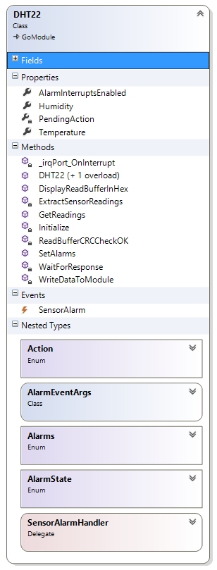
As with the STM8S code, the Netduino GO! driver is based upon the code developed previously and used as the basis for the Output Expander module. Much of this should be familiar and so we will only be considering the methods and supporting structures which implement specific features in this module. The class diagram for our module driver looks like this:
As you can see the module driver is not overly complex as it provides a few methods and supports a single interrupt.
The STM8S module returns temperature data on two occasions, the first is the explicit request by the Netduino GO! for the current readings, the second is when an alarm is raised. It therefore makes sense to abstract this code into a method:
/// <summary>
/// Extract the temperature and humidity data from the data which has been
/// generated by the STM8S.
/// </summary>
/// <param name="temperature">Temperature extracted from the buffer.</param>
/// <param name="humidity">Humidity extracted from the buffer.</param>
private void ExtractSensorReadings(out float temperature, out float humidity)
{
    //
    //  Verify the checksum before extracting the data.
    //
    int sum = 0;
    for (int index = 4; index < 8; index++)
    {
        sum += _readFrameBuffer[index];
    }
    if ((sum & 0xff) == _readFrameBuffer[8])
    {
        //
        //  Checksum good so extract the temperature and humidity data.
        //
        humidity = ((float) ((_readFrameBuffer[4] * 256) + _readFrameBuffer[5])) / 10;
        int sign = 1;
        byte highByte = _readFrameBuffer[6];
        if ((highByte & 0x80) == 0x80)
        {
            sign = -1;
            highByte &= (byte) 0x7f;
        }
        temperature = sign * ((float) ((highByte * 256) + _readFrameBuffer[7])) / 10;
    }
    else
    {
        throw new Exception("ExtractSensorData: Checksum error, discarding data.");
    }
}
The code which gets the current readings is relatively trivial:
/// <summary>
/// This method calls the AddOne method on the GO! module and then waits for the
/// module to indicate that there is a response ready.  The response is then read
/// from the module and the resulting value is returned to the caller.
/// </summary>
public void GetReadings()
{
    _writeFrameBuffer[0] = GO_BUS10_COMMAND_RESPONSE;
    _writeFrameBuffer[1] = (int) Action.GetReadings;
    WriteDataToModule();
    if (!WaitForResponse())
    {
        throw new Exception("GetReadings: Cannot communicate with the DHT22 module");
    }
}
Setting an alarm is also trivial, although the method is longer, with much of the work involving extracting the bytes of data and storing them in the transmit buffer:
/// <summary>
/// Set the alarms for the low/high temperature/humidity alarms.
/// </summary>
/// <remarks>
/// To turn an alarm off set the value to float.MinValue.
///
/// The alarms are triggered when the temperature/humidity goes below the low threshold
/// or above the high threshold.
/// </remarks>
/// <param name="lowTemperature">Low temperature alarm value.</param>
/// <param name="highTemperature">High temperature alarm value.</param>
/// <param name="lowHumidity">Low humidity alarm value.</param>
/// <param name="highHumidity">High humidity alarm value.</param>
public void SetAlarms(float lowTemperature, float highTemperature, float lowHumidity, float highHumidity)
{
    Alarms alarms = 0;

    if (lowTemperature != float.MinValue)
    {
        if ((lowTemperature < MIN_TEMPERATURE) || (lowTemperature > MAX_TEMPERATURE))
        {
            throw new ArgumentOutOfRangeException("SetAlarms: lowTemperature out of range.");
        }
        short lt = (short) (lowTemperature * 10);
        _writeFrameBuffer[3] = (byte) ((lt & 0xff00) >> 8);
        _writeFrameBuffer[4] = (byte) (lt & 0xff);
        alarms |= Alarms.LowTemperature;
    }
    if (highTemperature != float.MinValue)
    {
        if ((highTemperature > MAX_TEMPERATURE) || (highTemperature < MIN_TEMPERATURE))
        {
            throw new ArgumentOutOfRangeException("SetAlarms: highTemperature out of range.");
        }
        short ht = (short) (highTemperature * 10);
        _writeFrameBuffer[5] = (byte) ((ht & 0xff00) >> 8);
        _writeFrameBuffer[6] = (byte) (ht & 0xff);
        alarms |= Alarms.HighTemperature;
    }
    if (lowHumidity != float.MinValue)
    {
        if ((lowHumidity < MIN_HUMIDITY) || (lowHumidity > MAX_HUMIDITY))
        {
            throw new ArgumentOutOfRangeException("SetAlarms: lowHumidity out of range");
        }
        short lh = (short) (lowHumidity * 10);
        _writeFrameBuffer[7] = (byte) ((lh & 0xff00) >> 8);
        _writeFrameBuffer[8] = (byte) (lh & 0xff);
        alarms |= Alarms.LowHumidity;
    }
    if (highHumidity != float.MinValue)
    {
        if ((highHumidity < MIN_HUMIDITY) || (highHumidity > MAX_HUMIDITY))
        {
            throw new ArgumentOutOfRangeException("SetAlarms: highHumidity out of range");
        }
        short hh = (short) (highHumidity * 10);
        _writeFrameBuffer[9] = (byte) ((hh & 0xff00) >> 8);
        _writeFrameBuffer[10] = (byte) (hh & 0xff);
        alarms |= Alarms.HighHumidity;
    }
    _writeFrameBuffer[0] = GO_BUS10_COMMAND_RESPONSE;
    _writeFrameBuffer[1] = (int) Action.SetAlarms;
    _writeFrameBuffer[2] = (byte) alarms;
    WriteDataToModule();
    if (!WaitForResponse())
    {
        throw new Exception("SetAlarms: Cannot communicate with the DHT22 module");
    }
}
The really interesting work involves the receipt of data from the module. This is triggered by the interrupt being raised on the GPIO pin of the Netduino GO! connector.
/// <summary>
/// Handle the IRQ events generated by the GO! module.
/// </summary>
/// <remarks>
/// The module raises an interrupt when a command has been processed or when there
/// is data ready for the module.  The first task for this method is to retrieve
/// the buffer from the module and then work out what action should be taken.  The
/// module will have placed any relevant data into the write buffer prior to raising
/// the interrupt.
/// </remarks>
private void _irqPort_OnInterrupt(uint data1, uint data2, DateTime time)
{
    _writeFrameBuffer[0] = GO_BUS10_COMMAND_RESPONSE;
    _writeFrameBuffer[1] = (int) Action.GetBuffer;
    WriteDataToModule();
    if ((_readFrameBuffer[1] == GO_BUS10_COMMAND_RESPONSE) && (_readFrameBuffer[2] == DHT22_ACK) && ReadBufferCRCCheckOK())
    {
        float t, h;

        switch ((Action) _readFrameBuffer[3])
        {
            case Action.GetReadings:
                ExtractSensorReadings(out t, out h);
                Temperature = t;
                Humidity = h;
                _irqPortInterruptEvent.Set();
                break;
            case Action.SetAlarms:
                _irqPortInterruptEvent.Set();
                break;
            case Action.Alarm:
                if ((SensorAlarm != null) && (AlarmInterruptsEnabled == AlarmState.InterruptsEnabled))
                {
                    ExtractSensorReadings(out t, out h);
                    SensorAlarm(this, new AlarmEventArgs(t, h, (Alarms) _readFrameBuffer[9]));
                }
                break;
            default:
                throw new ArgumentException("Interrupt: Unknown action " + _readFrameBuffer[3].ToString());
                break;
        }
    }
}
This event allows the main program to set an alarm and then leave the module to work out when it needs to communicate with the Netduino GO!. This is achieved by the application setting the delegate SensorAlarm
Testing
At this point we have the hardware and software complete. All that is needed now is to put the two together:
A quick test application (I promise, this will be last piece of the code in this article):
The image above shows the DHT22 module connected to the Netduino GO!. A Komodex Labs Seven Segment Display is used to display the temperature and humidity.
And here is a video showing the module working. The system shows the temperature for a short while (16.8C) followed by the humidity (46.7%).
We were lucky last year as we had a particularly cold winter (lucky for testing). This allowed the module to be test outdoors in a reasonably cold environment. The sensor and the Netduino GO! performed as expected down to -10C when compared to an off the shelf digital thermometer and humidity unit. I would have waited for the temperature to drop further by my desire to prove the module has limits and I discovered that standing around outside with a coffee waiting for the module to read lower and lower temperatures had an interest threshold of about 10 minutes.
Conclusion
This module shows the power of combining microcontrollers to provide a combined system. The Netduino GO! would have found it difficult to have achieved the work completed by the STM8S. Similarly, the Netduino GO! provides the application developer with the simplicity and power of NETMF, something the STM8S could not achieve.
This module has yet to move from prototype into production. Maybe it will someday, just not today.
June 23rd, 2013 • Electronics, STM8 • Comments Off on Transmitting Data Using the STM8S SPI Master Mode
So far in The Way of the Register series we have only looked at SPI from a slave device point of view as we have been working towards creating a Netduino GO! module. For every slave device there must be a master, here we will look at configuring the STM8S to operate in SPI master mode.
The project will look at controlling a TLC5940 in order to emulate the work described in the post TLC5940 16 Channel PWM Driver. We could simply bit-bang the data out to the chip but instead we will use the SPI interface to achieve this.
The project breaks down into the following steps:
Generate the grey scale clock and blank signals
Bit-Bang data out over GPIO pins to create an operational circuit
Convert the data transmission to SPI
See the quoted post for a description of how this chip works and for an explanation of the terminology used.
Generating the Grey Scale Clock and Blank Signals
The TLC5940 generated 4,096 grey scale values by using a PWM counter. Once the counter reaches 4096 pulses it stops until it is told to restart. The Blank pulse acts as a restart signal. This project will be controlling LEDs and so will want to continuously keep the counter running. If we did not keep the counter in the TLC5940 running then the LEDs would light for a short while and then simply turn off and remain off.
The greyscale clock is generated by using the Configurable Clock Output (CCO) pin on the STM8S. This pin simply outputs the clock pulses used to drive the STM8S. Reviewing the data sheet we find that the maximum value for the grey scale clock is 30MHz. Using out standard clock initialisation generates a clock with a frequency of 16MHz (approximately). This is well within the tolerances of the TLC5940. To output this we need to make a simple modification to our standard code, name change the line:
CLK_CCOR = 0; // Turn off CCO.
to:
CLK_CCOR = 1; // Turn on CCO.
The starting point for our application becomes:
#if defined DISCOVERY
    #include <iostm8S105c6.h>
#elif defined PROTOMODULE
    #include <iostm8s103k3.h>
#else
    #include <iostm8s103f3.h>
#endif
#include <intrinsics.h>

//
//  Setup the system clock to run at 16MHz using the internal oscillator.
//
void InitialiseSystemClock()
{
    CLK_ICKR = 0;                       //  Reset the Internal Clock Register.
    CLK_ICKR_HSIEN = 1;                 //  Enable the HSI.
    CLK_ECKR = 0;                       //  Disable the external clock.
    while (CLK_ICKR_HSIRDY == 0);       //  Wait for the HSI to be ready for use.
    CLK_CKDIVR = 0;                     //  Ensure the clocks are running at full speed.
    CLK_PCKENR1 = 0xff;                 //  Enable all peripheral clocks.
    CLK_PCKENR2 = 0xff;                 //  Ditto.
    CLK_CCOR = 1;                       //  Turn on CCO.
    CLK_HSITRIMR = 0;                   //  Turn off any HSIU trimming.
    CLK_SWIMCCR = 0;                    //  Set SWIM to run at clock / 2.
    CLK_SWR = 0xe1;                     //  Use HSI as the clock source.
    CLK_SWCR = 0;                       //  Reset the clock switch control register.
    CLK_SWCR_SWEN = 1;                  //  Enable switching.
    while (CLK_SWCR_SWBSY != 0);        //  Pause while the clock switch is busy.
}

//
//  Main program loop.
//
void main()
{
    //
    //  Initialise the system.
    //
    __disable_interrupt();
    InitialiseSystemClock();
    __enable_interrupt();
    while (1)
    {
        __wait_for_interrupt();
    }
}
Wiring up the STM8S and connecting the scope to PC4 (CCO output pin) gives the following trace on the scope:
CCO On Scope
The trace on the scope has a minimum value of around 680mV and a maximum of 2.48V. In an ideal world this signal should range from 0 to 3.3V (based upon a 3.3V supply). Adding an inverter from a 74HC04 and feeding the signal through one of the gates gives the following trace:
Inverter output on the scope
This is starting to look a lot better. The next task is to create the Blank signal. There are several ways of doing this. The most automatic way of doing this is to generate a very short PWM pulse using one of the timers in the STM8S. One drawback of this method is that it is more difficult to generate a Blank pulse on demand. Instead we will use the interrupt method described in the same article. Whilst not automatic it is still a trivial task to complete. We simply modify the code from the method to load the counters with 4,096. The code for the GPIO port, timer and interrupt becomes:
//
//  Timer 2 Overflow handler.
//
#pragma vector = TIM2_OVR_UIF_vector
__interrupt void TIM2_UPD_OVF_IRQHandler(void)
{
    PD_ODR_ODR4 = 1;
    PD_ODR_ODR4 = 0;
    TIM2_SR1_UIF = 0;       //  Reset the interrupt otherwise it will fire again straight away.
}

//
//  Setup Timer 2 to generate an interrupt every 4096 clock ticks.
//
void SetupTimer2()
{
    TIM2_PSCR = 0x00;       //  Prescaler = 1.
    TIM2_ARRH = 0x10;       //  High byte of 4096.
    TIM2_ARRL = 0x00;       //  Low byte of 4096.
    TIM2_IER_UIE = 1;       //  Turn on the interrupts.
    TIM2_CR1_CEN = 1;       //  Finally enable the timer.
}

//
//  Setup the output ports used to control the TLC5940.
//
void SetupOutputPorts()
{
    PD_ODR = 0;             //  All pins are turned off.
    PD_DDR_DDR4 = 1;        //  Port D, pin 4 is used for the Blank signal.
    PD_CR1_C14 = 1;         //  Port D, pin 4 is Push-Pull
    PD_CR2_C24 = 1;         //  Port D, Pin 4 is generating a pulse under 2 MHz.
}
Hooking up the scope to PD4 gives the following trace:
Blanking pulses
The single pulses are being generated at a frequency of approximately 3.9kHz. A little mental arithmetic dividing the 16MHz clock by 4,096 comes out to about 3,900.
Zooming in on the signal we see:
Single Blanking Pulse
This shows that the signal is 125nS wide. This is acceptable as the minimum pulse width given in the data sheet is 20nS.
So at this point we have the 16MHz grey scale clock signal and the Blank pulse being generated every 4,096 clock pulses.
Connecting the TLC5940
The next task is to connect the STM8S to the TLC5940. You should refer to the article TLC5940 16 Channel PWM Driver for more information on the pins and their meaning. For this exercise we will use the following mapping:
STM8S Pin
TLC5940 Pin
PD4
Blank (pin 23)
PD3
XLAT (pin 24)
PD2
VPRG (pin 27)
PD5
Serial data (pin 26)
PD6
Serial clock (pin 25)
PC4 (via inverter)
GSCLK (pin 18)
You will note that the serial data and clock are currently connected to PD5 and PD6 respectively. Whilst the eventual aim is to communicate with the TLC5940 via SPI, the initial communication will be using Bit-Banging. We will move on to using SPI once the operation of the circuit has been proven using tested technology.
The first changes we will have to make create some #define statements to make the code a little more readable. We also add some storage space for the grey scale and dot correction data.
//
//  Define which pins on Port D will be used as control signals for the TLC5940.
//
//  BLANK - A pulse from low to high causes the TLC5940 to restart the counter
//  XLAT - A high pulse causes the data to be transferred into the DC or GS registers.
//  VPRG - Determines which registers are being programmed, High = DC, Low = GS.
//
#define PIN_BLANK                   PD_ODR_ODR4
#define PIN_XLAT                    PD_ODR_ODR3
#define PIN_VPRG                    PD_ODR_ODR2
//
//  Bit bang pins.
//
#define PIN_BB_DATA                 PD_ODR_ODR5
#define PIN_BB_CLK                  PD_ODR_ODR6
//
//  Values representing the modes for the VPRG pin.
//
#define PROGRAMME_DC                1
#define PROGRAMME_GS                0

//
//  TLC5940 related definitions.
//
#define TLC_NUMBER                  1
#define TLC_DC_BYTES_PER_CHIP       12
#define TLC_DC_BYTES                TLC_NUMBER * TLC_DC_BYTES_PER_CHIP
#define TLC_GS_BYTES_PER_CHIP       24
#define TLC_GS_BYTES                TLC_NUMBER * TLC_GS_BYTES_PER_CHIP

//
//  Next we need somewhere to hold the data.
//
unsigned char _greyScaleData[TLC_GS_BYTES];
unsigned char _dotCorrectionData[TLC_DC_BYTES];
The Bit-Banging methods should look familiar to anyone who has been reading any of the posts in The Way of the Register series.
//--------------------------------------------------------------------------------
//
// Bit bang data.
//
// TLC5940 expects the data to be shifted MSB first. The data
// is shifted in on the rising edge of the clock.
//
void BitBang(unsigned char byte)
{
for (short bit = 7; bit >= 0; bit--)
{
if (byte & (1 << bit))
{
PIN_BB_DATA = 1;
}
else
{
PIN_BB_DATA = 0;
}
PIN_BB_CLK = 1;
PIN_BB_CLK = 0;
}
PIN_BB_DATA = 0;
}
//--------------------------------------------------------------------------------
//
// Bit bang a buffer of data.
//
void BitBangBuffer(unsigned char *buffer, int size)
{
for (int index = 0; index < size; index++)
{
BitBang(buffer[index]);
}
}
Related to the Bit-Banging methods are the two methods which will send the grey scale and dot correction data:
//--------------------------------------------------------------------------------
//
//  Send the grey scale data to the TLC5940.
//
void SendGreyScaleData(unsigned char *buffer, int length)
{
    PIN_VPRG = PROGRAMME_GS;
    BitBangBuffer(buffer, length);
    PulseXLAT();
    PulseBlank();
}

//--------------------------------------------------------------------------------
//
//  Send the dot correction buffer to the TLC5940.
//
void SendDotCorrectionData(unsigned char *buffer, int length)
{
    PIN_VPRG = PROGRAMME_DC;
    BitBangBuffer(buffer, length);
    PulseXLAT();
    PulseBlank();
}
We also need a few methods to make the TLC5940 latch the data and also restart the counters:
//--------------------------------------------------------------------------------
//
//  Pulse the Blank pin in order to make the TLC5940 reload the counters and
//  restart timer.
//
void PulseBlank()
{
    PIN_BLANK = 1;
    PIN_BLANK = 0;
}

//--------------------------------------------------------------------------------
//
//  Pulse the XLAT pin in order to make the TLC5940 transfer the
//  data from the latches into the appropriate registers.
//
void PulseXLAT()
{
    PIN_XLAT = 1;
    PIN_XLAT = 0;
}
Next we need to set the initial condition. For this we set the TLC dot correction off and also turn all of the LEDs off:
//--------------------------------------------------------------------------------
//
//  Initialise the TLC5940.
//
void InitialiseTLC5940()
{
    for (int index = 0; index < TLC_DC_BYTES; index++)
    {
        _dotCorrectionData[index] = 0xff;
    }
    for (int index = 0; index < TLC_GS_BYTES; index++)
    {
        _greyScaleData[index] = 0;
    }
    SendDotCorrectionData(_dotCorrectionData, TLC_DC_BYTES);
    SendGreyScaleData(_greyScaleData, TLC_GS_BYTES);
}
The final support method we need to add is the method which sets the brightness of an LED. The brightness is a 12-bit value (0-4095). This means each LED uses 1.5 bytes for the brightness value. The following methods breaks down the value and ensures that the correct bits are set in the grey scale buffer depending upon which LED is being changed:
//--------------------------------------------------------------------------------
//
//  Set the brightness of an LED.
//
void SetLEDBrightness(int ledNumber, unsigned short brightness)
{
    int offset = (ledNumber >> 1) * 3;
    if (ledNumber & 0x01)
    {
        _greyScaleData[offset + 1] = (unsigned char) (_greyScaleData[offset + 1] & 0xf0) | ((brightness & 0x0f00) >> 8);
        _greyScaleData[offset + 2] = (unsigned char) (brightness & 0xff);
    }
    else
    {
        _greyScaleData[offset] = (unsigned char) ((brightness & 0x0ff0) >> 4) & 0xff;
        _greyScaleData[offset + 1] = (unsigned char) ((brightness & 0x0f) >> 4) | (_greyScaleData[offset + 1] & 0x0f);
    }
}
We should also create a similar method for changing the dot correction value for an LED. This is left as an exercise for the reader as we will not be changing this value in this code.
Proving the concept
If we have connected the TLC5940 correctly and our code works we should be able to connect up some LEDs (common anode) to the TLC5940 and change the brightness under program control.
This main program loop slowly increases the brightness of the LEDs. When they are at full brightness they are turned off and the process starts again:
//--------------------------------------------------------------------------------
//
//  Main program loop.
//
void main()
{
    //
    //  Initialise the system.
    //
    __disable_interrupt();
    InitialiseSystemClock();
    SetupOutputPorts();
    SetupTimer2();

    InitialiseTLC5940();
    __enable_interrupt();
    //
    //  Main program loop.
    //
    int brightness = 0;
    int counter = 0;
    while (1)
    {
        __wait_for_interrupt();
        counter++;
        if (counter == 20)
        {
            TIM2_CR1_CEN = 0;
            counter = 0;
            for (int index = 0; index < 16; index++)
            {
                SetLEDBrightness(index, brightness);
            }
            SendGreyScaleData(_greyScaleData, TLC_GS_BYTES);
            brightness++;
            if (brightness == 4096)
            {
                brightness = 0;
            }
            TIM2_CR1_CEN = 1;       //  Finally re-enable the timer.
        }
    }
}
If you connect a scope to the cathode of one of the LEDs you will see that the wave form slowly changes over time. At the start, the LED is fully on and the trace on the scope shows a horizontal line, i.e. a constant voltage. As time moves on and the value in the dot correction buffer changes you start to see a PWM signal similar to the following:
PWM Output On Scope 1
This trace shows the signal when the LEDs are a little brighter:
PWM Output On Scope 2
Having arrived here we now know that the circuit has been connected correctly and that the control logic in the main method works. We can now move on to considering what we need to do in order to use SPI in master mode. The aim will be to simply remove the Bit-Banging methods and replace these with an interrupt driven SPI master algorithm.
SPI Master
So now we have a working circuit we need to look at SPI on the STM8S. Firstly let’s remind ourselves of the serial communication parameters for the TLC5940. This chip reads the data on the leading clock edge (CPHA = 1). We have also set the clock idle state to low (CPOL = 0).
It is also advisable to start off using the lowest clock speed for SPI in order to confirm correct operation of the software and circuit. Lower speed are less likely to be subject to interference.
SPI Registers
You should review the previous articles on SPI communication if you are not already familiar with the SPI registers we have used so far. In this post we will only discuss the new settings required to switch from being a SPI slave device to a SPI master device.
SPI_CR1_BR – Baud Rate Control
The SPI baud rate is determined by the master clock frequency and the value in this register. The divisor used to set the baud rate according to the following table:
SPI_CR1_BR
Divisor
000
2
001
4
010
8
011
16
100
32
101
64
110
128
111
256
The SPI baud rate is calculated as fmaster / divisor. So for our master clock speed of 16MHz we get the lowest clock speed of 16,000,000 / 256, or 62,500Hz.
SPI_CR1_MSTR – Master Selection
Setting this bit switches SPI into master mode (see also SPI_CR1_SPE).
Note that the reference for the STM8S also states that this bit (and SPI_CR1_SPE) will only remain set whilst NSS is high. It this therefore essential to connect NSS to Vcc if this device is not being used as a slave device.
Implementing SPI
Using SPI presents us with a small problem, namely the program will have to start to operate in a more asynchronous way. The code presented so far has only one interrupt to be concerned with, namely the timer used to control the Blank signal. Adding SPI to the mix means that we will have to also consider the SPI interrupt as well. It also adds the complication of sending dot correction data followed by grey scale data. This last problem will not be covered here and is left as an exercise for the reader.
The initialisation code merely sets things up for us:
//--------------------------------------------------------------------------------
//
//  Initialise SPI to be SPI master.
//
void SetupSPIAsMaster()
{
    SPI_CR1_SPE = 0;                    //  Disable SPI.
    SPI_CR1_CPOL = 0;                   //  Clock is low when idle.
    SPI_CR1_CPHA = 0;                   //  Capture MSB on first edge.
    SPI_ICR_TXIE = 1;                   //  Enable the SPI TXE interrupt.
    SPI_CR1_BR = 7;                     //  fmaster / 256 (62,500 baud).
    SPI_CR1_MSTR = 1;                   //  Master device.
}
Much of the code should be familiar as it has been used in previous posts discussing SPI slave devices. Not however that we do not enable SPI at this point. We simply set the scene for us to use SPI later.
The SPI data transfers will be controlled by using an interrupt service routine:
//--------------------------------------------------------------------------------
//
//  SPI Interrupt service routine.
//
#pragma vector = SPI_TXE_vector
__interrupt void SPI_IRQHandler(void)
{
    //
    //  Check for an overflow error.
    //
    if (SPI_SR_OVR)
    {
        (void) SPI_DR;                      // These two reads clear the overflow
        (void) SPI_SR;                      // error.
        return;
    }
    if (SPI_SR_TXE)
    {
        //
        //  Check if we have more data to send.
        //
        if (_txBufferIndex == _txBufferSize)
        {
            while (SPI_SR_BSY);
            SPI_CR1_SPE = 0;
            _txBuffer = 0;
            PulseXLAT();
            PulseBlank();
            TIM2_CR1_CEN = 1;
        }
        else
        {
            SPI_DR = _txBuffer[_txBufferIndex++];
        }
    }
}
The main works starts when we have established that the transmit buffer is empty (SPI_SR_TXE is set). If we have more data then we put the byte into the data register (SPI_DR). If we have transmitted all the data we have then we wait for the last byte to complete transmission (SPI_SR_BSY becomes false) before we start to terminate the end of the SPI communication.
In order to send some data we really just need to setup the pointers and counters correctly and then enable SPI. So the SendGreyScaleData method becomes:
//--------------------------------------------------------------------------------
//
//  Send the grey scale data to the TLC5940.
//
void SendGreyScaleData(unsigned char *buffer, int length)
{
    PIN_VPRG = PROGRAMME_GS;
    _txBuffer = buffer;
    _txBufferIndex = 0;
    _txBufferSize = length;
    TIM2_CR1_CEN = 0;
    SPI_CR1_SPE = 1;
}
We also need to have a look at the main program loop as we use the __wait_for_interrupt() method in order to determine when we should start to process the next LED brightness value. We now need to ignore the interrupts when SPI is enabled otherwise the brightness will increase each time the transmit buffer is empty. A crude implementation eliminating the SPI interrupts is:
int brightness = 0;
int counter = 0;
while (1)
{
    __wait_for_interrupt();
    if (!SPI_CR1_SPE)
    {
        counter++;
        if (counter == 20)
        {
            TIM2_CR1_CEN = 0;
            counter = 0;
            for (int index = 0; index < 16; index++)
            {
                SetLEDBrightness(index, brightness);
            }
            SendGreyScaleData(_greyScaleData, TLC_GS_BYTES);
            brightness++;
            if (brightness == 4096)
            {
                brightness = 0;
            }
            TIM2_CR1_CEN = 1;       //  Finally re-enable the timer.
        }
    }
}
Making these changes and running the code shows that the system operated as before.
Increasing the Baud Rate
As noted earlier, the baud rate has been set low in order to reduce the chance of any problems being experienced due to interference. Now we have established that using SPI communication is possible and the circuit works as before we can start to increase the baud rate. Using our 16MHz clock we find we have the following baud rates which are theoretically possible:
SPI_CR1_BR
Divisor
SPI Frequency
000
2
8 MHz
001
4
4 MHz
010
8
2 MHz
011
16
1 MHz
100
32
500 KHz
101
64
250 KHz
110
128
125 KHz
111
256
62.5 KHz
A little experimentation is called for. Being ambitious I started with a clock frequency of 1MHz. This resulted in a flickering effect on the LED display. So, 1MHz is too ambitious, let’s start to reduce the frequency. I finally settled on 250 KHz as this allowed the circuit to function as before.
Conclusion
Using SPI master for data transmission was not as difficult as I originally thought. To make this application complete there are a few tasks to follow up on, namely:
Receiving data over SPI
Create the method to allow setting the dot correction values
Transmitting buffers from a queue
Minor tidying up of the timer control
The use of SPI here actually increased the time taken (597uS Bit-Banging c.f. 795uS for 250 KHz SPI) to reliably send the grey scale data to the TLC5940. I suspect that the time can be decreased if the circuit was taken from breadboard and put onto a PCB manufactured for the purpose. The breadboard for this circuit currently looks like this:
Bread Board And Flying Leads
As you can see, there is a lot of opportunity for interference with all those flying leads.
While the time taken might have increased, the load on the microcontroller will have decreased as the SPI method is interrupt driven. The actual transmission is off-loaded to the microcontrollers dedicated circuitry.
June 3rd, 2013 • General • Comments Off on How much would you pay?
One of the joys of being a hobbyist is the fact that you can take a project as far as you want to. Something really fun nearly always remains fun and does not make any money. As long as it’s a hobby it does not really matter.
So what do you do when you want to make money from your hobby. This is the question which Michael Ciuffo of ch00ftech found himself addressing with his QR Clock project earlier this year.
I’d check out The Slowest $380 I’ll Ever Make post for advice on the pros and cons of taking a hobby idea from concept to production.
Regular readers will know that I rarely post links to other peoples work but I feel that I should share this post as much of the post resonates with me. The Output Expander project was for me a great exercise as I had never taken a project from concept through to professional PCB manufacture. Having done this I was left with a simple question – could I make some extra money from this?
I think Michael’s post answers this question and it’s well worth reading.
Sometimes you have to do something just because you can. Today was no exception. Take one Raspberry Pi board (Linux) and give it a dose of .NET loving…
I can hear people screaming NO! but it’s too late, I’ve done it.
To be honest, I’m not the first person to use .NET on the Raspberry Pi. In fact I used this installation guide to install Mono on the Raspberry Pi.
So what interested me? Simply put, hardware interfacing. Could the .NET hardware classes (i.e. SerialPort) be used on the Raspberry Pi? There was only one way to find out.
Raspberry Pi Setup
The first thing to do was to set up the Raspberry Pi using the instructions in the blog mentioned above. This was not difficult although it was time consuming as it took a while to compile.
When this is complete a simple program should demonstrate if the serial ports are available to us. The following code should show this:
namespace ConsoleApplication1
{
	class Program
	{
		public static void Main(string[] args)
		{
			SerialPort sp = new SerialPort("/dev/ttyAMA0", 115200, Parity.None, 8, StopBits.One);
			sp.Open();
			for (int index = 0; index < 10; index++)
			{
				string result = string.Format("{0} Testing", index);
				sp.Write(result);
			}
			sp.Close();
		}
	}
}
As you can see, this code is not too complex. It merely opens a serial port and then starts to output data to the port. The only tricky part of the job was to locate the name to be used for the serial port. It’s been too long since I used Unix in anger.
Testing the Application
Testing is not too complex as the test application is simply outputting a text message. We can see the output by hooking up PuTTY to a serial port on a computer.
The hardware is also simple to hook up. The FTDI cable I have allows me to connect a 3.3V TTL serial device to my PC over USB. This USB device then appears as a standard serial device on the PC. Three connections are required:
Raspberry Pi
FTDI Cable
Ground
Ground
Rx
Tx
Tx
Rx
Strictly speaking, we do not have to connect the Tx on the FTDI cable to the Rx on the Raspberry Pi as we will not be transmitting anything from the PC to the Raspberry Pi in this example.
Once the hardware is connected you will need to fire up PuTTY and connect it to the serial port on your PC. Ensure that the settings used match those in the application code above.
Assuming that you now have Mono installed and the application typed in ready to go, type the following commands into a shell on the Raspberry Pi:
mcs serial.cs
mono serial.exe
The first command invokes the Mono C# compiler. The second tells mono to execute the application which has been compiled.
If all has gone well then you will see something like this in the PuTTY window running on the PC:
Serial Output in Putty
Conclusion
I was rather interested to see that the C# skills acquired on the PC could also be used on the Raspberry Pi. The only thing missing on the Pi was a good development environment.
This website uses cookies to improve your experience and to gather page view statistics. This site does not collect user information. Accept & CloseRead More
Privacy & Cookies Policy
Privacy Overview
This website uses cookies to improve your experience while you navigate through the website. Out of these, the cookies that are categorized as necessary are stored on your browser as they are essential for the working of basic functionalities of the website. We also use third-party cookies that help us analyze and understand how you use this website. These cookies will be stored in your browser only with your consent. You also have the option to opt-out of these cookies. But opting out of some of these cookies may affect your browsing experience.
Necessary cookies are absolutely essential for the website to function properly. This category only includes cookies that ensures basic functionalities and security features of the website. These cookies do not store any personal information.
Any cookies that may not be particularly necessary for the website to function and is used specifically to collect user personal data via analytics, ads, other embedded contents are termed as non-necessary cookies. It is mandatory to procure user consent prior to running these cookies on your website.