RSS

Archive for the ‘Home Built CPU’ Category

SSEM Program Execution Complete

Wednesday, July 19th, 2023

SSEM Program Execution Complete

A while ago I put together an emulator for the Small Scale Experimental Machine (SSEM), also known as the Manchester Baby. This was a basic console application allowing a program written for the Manchester Baby to be run in a console application on a modern computer. As things turned out, I now spend most of my time working in either C or C++. This has left me with a piece of code that is difficult to maintain as I have to relearn Python every time I want to make any improvements.

Time to rewrite the application in C++.

SSEM Simulator

The simulator provides a number of features:

  • Assembler/compiler to take source files and generate the binary to be execution
  • Console interface to control the execution of the application
  • Simulated display of the registers and memory

More information about the Python version of the simulator can be found in this blog and on the Small Scale Experimental Machine web site with full source code available on GitHub.

Porting the Simulator

The aim of the initial port is to provide the same functionality of the original application with any changes necessary to provide additional robustness as we are undoubtedly going to be seeing pointers in the C++ port.

Where possible, the structure of the original Python code has been maintained to keep a 1:1 mapping with the original code and test suite. This will provide an easy way to validate the unit tests in the port against the original Python code. The original Python code was validated against David Sharps Java Simulator.

The long term aim of this port is to provide a way of running the application on a Raspberry Pi Pico connected to hardware which will emulate the original SSEM. The application on the Raspberry Pi Pico will target the NuttX RTOS. As we will see later, compiling and running on NuttX will present some interesting issues.

Initial Port

The first stage of the port is to reproduce the core functionality of the SSEM showing the application output in a console interface targeting C++ 17. The only real complication here is ensure the user interface and platform specific code are abstracted to keep as much functionality in common with a desktop and NuttX implementation as possible.

The original Python code and the C++ port can be found in the Manchester Baby GitHub repository. A quick check of the source code shows that the 1:1 mapping has been kept where possible. The only real significant difference between the two code bases is the separation of the unit tests from the class implementation. The Python code keeps the unit test code in the class definitions themselves, the C++ code implements the unit tests in their own files.

Memory Checks

The switch from Python to C++ brings a new danger, memory access issues and memory leaks.

One memory issue that we can address relatively easily is memory leaks. If we can abstract the core functionality into a self contained group of files then we can use valgrind to check for memory leaks. A small glitch with using valgrind is that the application is not available for Mac from the key repositories. There is an informal project on GitHub.

The issue of valgrind not running on the mach was resolved by putting together a Dockerfile containing common development tools. The memory check could then be run on the desktop using Docker.

Running the Emulator

The emulator can be run on both a desktop computer as well as a board running NuttX.

Run from the Desktop

Running the application on the desktop is the simplest way to test the emulator:

  • Open a command console and change to the Desktop directory in the repository
  • Build the emulator with the command make
  • Run the emulator with the command ./ssem_main

Run on NuttX

Running on NuttX is a little more complex as we need to build the application and the operating system and then deploy the binary to a board. The processes of adding the SSEM application to a Raspberry Pi PicoW board has already been documented in the article Adding a User Application to NuttX. The first step is to follow the steps in the article to add the SSEM basic applicatiom.

The next stage is to copy the contents of the NuttX directory over the application directory created in the above article. The code should then be rebuilt with the command make clean && make -j. The application can now be deployed to the board.

Now we have the OS and the application deployed to the Raspberry Pi (or your board of choice) we can connect a serial adapter to the board and press the enter key twice. This will bring up the NuttX shell. Typing help should show the ssem application deployed to the board. Simply execute this by entering the command ssem.

Application Output

In both cases the emulator should run the hfr989.ssem application (the source for this can be found in the SSEMApps folder in the repository). Both the desktop and the NuttX versions of the emulator will run the SSEM application and will show the start and end state of the SSEM on the console / serial port. The first output will show the SSEM application loaded into the store lines:

NuttShell (NSH) NuttX-10.4.0
nsh> ssem
                   00000000001111111111222222222233
                   01234567890123456789012345678901
   0: 0x00000000 - 00000000000000000000000000000000 JMP 0            ; 0
   1: 0x48020000 - 01001000000000100000000000000000 LDN 18           ; 16402
   2: 0xc8020000 - 11001000000000100000000000000000 LDN 19           ; 16403
   3: 0x28010000 - 00101000000000010000000000000000 SUB 20           ; 32788
   4: 0x00030000 - 00000000000000110000000000000000 CMP              ; 49152
   5: 0xa8040000 - 10101000000001000000000000000000 JPR 21           ; 8213
   6: 0x68010000 - 01101000000000010000000000000000 SUB 22           ; 32790
   7: 0x18060000 - 00011000000001100000000000000000 STO 24           ; 24600
   8: 0x68020000 - 01101000000000100000000000000000 LDN 22           ; 16406
   9: 0xe8010000 - 11101000000000010000000000000000 SUB 23           ; 32791
  10: 0x28060000 - 00101000000001100000000000000000 STO 20           ; 24596
  11: 0x28020000 - 00101000000000100000000000000000 LDN 20           ; 16404
  12: 0x68060000 - 01101000000001100000000000000000 STO 22           ; 24598
  13: 0x18020000 - 00011000000000100000000000000000 LDN 24           ; 16408
  14: 0x00030000 - 00000000000000110000000000000000 CMP              ; 49152
  15: 0x98000000 - 10011000000000000000000000000000 JMP 25           ; 25
  16: 0x48000000 - 01001000000000000000000000000000 JMP 18           ; 18
  17: 0x00070000 - 00000000000001110000000000000000 HALT             ; 57344
  18: 0x00000000 - 00000000000000000000000000000000 JMP 0            ; 0
  19: 0xc43fffff - 11000100001111111111111111111111 HALT             ; -989
  20: 0x3bc00000 - 00111011110000000000000000000000 JMP 28           ; 988
  21: 0xbfffffff - 10111111111111111111111111111111 HALT             ; -3
  22: 0x243fffff - 00100100001111111111111111111111 HALT             ; -988
  23: 0x80000000 - 10000000000000000000000000000000 JMP 1            ; 1
  24: 0x00000000 - 00000000000000000000000000000000 JMP 0            ; 0
  25: 0x08000000 - 00001000000000000000000000000000 JMP 16           ; 16
  26: 0x00000000 - 00000000000000000000000000000000 JMP 0            ; 0
  27: 0x00000000 - 00000000000000000000000000000000 JMP 0            ; 0
  28: 0x00000000 - 00000000000000000000000000000000 JMP 0            ; 0
  29: 0x00000000 - 00000000000000000000000000000000 JMP 0            ; 0
  30: 0x00000000 - 00000000000000000000000000000000 JMP 0            ; 0
  31: 0x00000000 - 00000000000000000000000000000000 JMP 0            ; 0

Reading from left to right, the above output shows the following:

  • Store line number (i.e. the memory address) 0:, 1: etc.
  • The hexadecimal representation of the store line contents.
  • Binary representation of the store line contents
  • Disassembled representation of the store line contents JMP 0 etc.
  • Decimal representation of the store line contents

It must be remembered when reading the above that the least significant bit is at the left of the word and the most significant bit is to the right. This is honoured with the hexadecimal and binary components of the above output. The decimal value to the right should be read in the usual way for a base 10 number.

After a short time the contents of the store lines at the end of the run will be displayed:

Program execution complete.
                   00000000001111111111222222222233
                   01234567890123456789012345678901
   0: 0x00000000 - 00000000000000000000000000000000 JMP 0            ; 0
   1: 0x48020000 - 01001000000000100000000000000000 LDN 18           ; 16402
   2: 0xc8020000 - 11001000000000100000000000000000 LDN 19           ; 16403
   3: 0x28010000 - 00101000000000010000000000000000 SUB 20           ; 32788
   4: 0x00030000 - 00000000000000110000000000000000 CMP              ; 49152
   5: 0xa8040000 - 10101000000001000000000000000000 JPR 21           ; 8213
   6: 0x68010000 - 01101000000000010000000000000000 SUB 22           ; 32790
   7: 0x18060000 - 00011000000001100000000000000000 STO 24           ; 24600
   8: 0x68020000 - 01101000000000100000000000000000 LDN 22           ; 16406
   9: 0xe8010000 - 11101000000000010000000000000000 SUB 23           ; 32791
  10: 0x28060000 - 00101000000001100000000000000000 STO 20           ; 24596
  11: 0x28020000 - 00101000000000100000000000000000 LDN 20           ; 16404
  12: 0x68060000 - 01101000000001100000000000000000 STO 22           ; 24598
  13: 0x18020000 - 00011000000000100000000000000000 LDN 24           ; 16408
  14: 0x00030000 - 00000000000000110000000000000000 CMP              ; 49152
  15: 0x98000000 - 10011000000000000000000000000000 JMP 25           ; 25
  16: 0x48000000 - 01001000000000000000000000000000 JMP 18           ; 18
  17: 0x00070000 - 00000000000001110000000000000000 HALT             ; 57344
  18: 0x00000000 - 00000000000000000000000000000000 JMP 0            ; 0
  19: 0xc43fffff - 11000100001111111111111111111111 HALT             ; -989
  20: 0x54000000 - 01010100000000000000000000000000 JMP 10           ; 42
  21: 0xbfffffff - 10111111111111111111111111111111 HALT             ; -3
  22: 0x6bffffff - 01101011111111111111111111111111 HALT             ; -42
  23: 0x80000000 - 10000000000000000000000000000000 JMP 1            ; 1
  24: 0x00000000 - 00000000000000000000000000000000 JMP 0            ; 0
  25: 0x08000000 - 00001000000000000000000000000000 JMP 16           ; 16
  26: 0x00000000 - 00000000000000000000000000000000 JMP 0            ; 0
  27: 0x00000000 - 00000000000000000000000000000000 JMP 0            ; 0
  28: 0x00000000 - 00000000000000000000000000000000 JMP 0            ; 0
  29: 0x00000000 - 00000000000000000000000000000000 JMP 0            ; 0
  30: 0x00000000 - 00000000000000000000000000000000 JMP 0            ; 0
  31: 0x00000000 - 00000000000000000000000000000000 JMP 0            ; 0
Executed 21387 instructions in 30000000 nanoseconds

The original SSEM ran at about 700 instructions per second, modern PCs and even RP2040 processors are running the application much faster.

Conclusion

Even small boards (such as the Raspberry Pi Pico) running relatively low power processors can now emulate the Manchester Baby running application intended for the SSEM many times faster that the original hardware. The hfr989.ssem application would have run in about 30 seconds in 1948, today we can run this in an emulator in less that 30ms.
NE555 Variable Speed Clock

Sunday, February 9th, 2020

The first post about the NE555 presented the theory of operation of the NE555 using an astable clock circuit. This circuit is the basis of a simple low frequency (by todays standards) digital clock or PWM circuit. A clock can be used to synchronise the various components in a digit circuit and PWM is useful in circuits for such things as light (LED) brightness.

This post will look at how the circuit in the first post can be modified to provide a variable clock for a digital circuit. A variable clock can prove useful when debugging a digital circuit.

Basic Astable Circuit

A simple astable circuit looks something like the following:

Astable Logical Layout

Astable Logical Layout

The two resistors R1, R2 and the capacitor control the timing and characteristics of the pulses seen on the output pin of the NE555.

Timing Calculations

The timing calculations given in the data sheet for the NE555 are as follows.

Note that in the following calculations, resistance is expressed on Ohms, capacitance in Farads and time in seconds.

Charge Time

The charge time depends upon the capacitor and the two resistors R1 and R2 as current flows through the two resistors to charge the capacitor. The time taken to charge is given as:

tcharge = 0.693 * (R1 + R2) * C

Discharge Time

The discharge time is only dependent upon the capacitor and R2 as current does not flow through R1 when the circuit is discharging. The time take to discharge is given as:

tdischarge = 0.693 * R2 * C

Period

The period is the sum of the two timings tcharge and tdischarge. This can be expressed as:

Period = 0.693 * (R1 + (2 * R2)) * C

Frequency

The frequency of a signal is defined as 1/Period. The period of a signal from an astable NE555 is:

Frequency = 1.44 / ((R1 + 2 * R2) * C)

Duty Cycle

The duty cycle of a signal is the percentage of time the signal is high compared to the period of the signal. Thus the duty cycle is given by the following formula:

Duty Cycle (%) = 100 * (R1 + R2) / (R1 + 2 * R2)

Fixed Clock

A fixed clock can be set up easily by changing one or more of the two resistors R1, R2 or the capacitor and a simple spreadsheet will allow you to calculate the circuit characteristics. Doing this allows for the creation of a low (by modern standards) frequency clock quickly and cheaply.

Variable Clock

A variable clock can be useful in debugging digital circuits. The ability to slow the speed of the system can allow the system to be probed easily while maintaining the ability to run the circuit using a free running clock.

As with a fixed clock, the clock characteristics can be changed by varying the value of one or more of R1, R2 or the capacitor.

Variable capacitors and resistors are both available but variable resistors (potentiometers) are more readily available to the hobbyist and so we will follow this option.

This gives two options, changing R1 or R2. Looking at the calculations above it is clear that R2 has the most impact on virtually every operating characteristic of the NE555 and is the only one that can influence the discharge time.

Looking at the tdischarge formula:

tdischarge = 0.693 * R2 * C

the discharge time could theoretically be reduced to zero if R2was allowed to approach 0 Ohms. This can be prevented by replacing R2 with a combination of a fixed value resistor and a potentiometer. The fixed resistor provides for a lower limit for the discharge time of the capacitor.

A quick spreadsheet shows how the circuit will behave as R2 and C are varied:

NE555 Calculations

NE555 Calculations

From the results above it looks like a minimum value for R2 of 1 KOhm and a maximum of 100 KOhm would give a reasonable frequency for a low speed clock.

Schematic

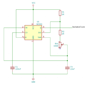
Lowering the value of R2 1 KOhm and adding a 100 KOhm potentiometer results in the following schematic:

Schematic for a variable speed clock using the NE555 timer

Variable Speed Clock Schematic

The value of the fixed resistor and the potentiometer gives a range of 1 KOhm to 101 KOhm. The additional 1 KOhm of resistance should not impact the frequency too much when the potentiometer is set to its maximum resistance as the calculation is dominated by the 100 KOhm potentiometer.

So that is the theory, how does this work in practice?

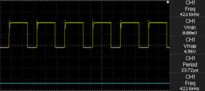
Potentiometer Set to 0 Ohms

If we set the potentiometer to 0 Ohms then according to the calculations above, the frequency should be about 48 KHz. The output on the oscilloscope is:

Oscilloscope output when potentiometer set to 0 Ohm

Potentiometer set to 0 Ohm

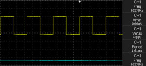
Potentiometer Set to 100 KOhms

Changing the potentiometer to 100 KOhms we should get a frequency of 712 Hz. The output on the oscilloscope is:

Oscilloscope output when potentiometer set to 100 KOhm

Oscilloscope output when potentiometer set to 100 KOhm

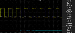
And Somewhere in the Middle

By slowly changing the resistance of the potentiometer we can achieve a steady slow clock of approximately 1 kHz:

NE555 generating a 1 KHz signal

NE555 generating a 1 KHz signal

Conclusion

Clocks provide the heartbeat of most digital circuits, computers certainly require a regular pulse to synchronise the various components in the circuit. The NE555 provides a simple way to generate a variable clock albeit at low frequencies.

The output on the oscilloscope varies from the ideal values given by the calculations. This can be explained by the variations in the tolerances of the various components in the circuits and from the capacitance of the breadboard itself.

NE555 Theory of Operation

Wednesday, July 17th, 2019

Oscilloscope Trace

Oscilloscope Trace

Ohhhh no, not another post about the NE555 timer! I’m sorry to say, yes, this is another article (or two) about the NE555, how it works and some applications.

I blog for two main reasons:

  • As an aide-memoire
  • Hopefully others will find these posts useful

So this first post will cover the theory behind the operation of the NE555 using the astable circuit as an example.

Logical Layout of the NE555

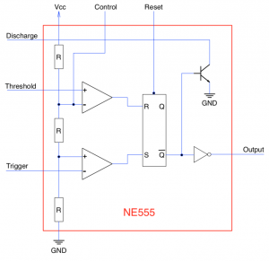
The NE555 has four logical units and they can be viewed logically in the following layout:

Logical units with NE555

NE555 Logical Layout

These logical units are:

  1. Resistor ladder
  2. Two comparators
  3. S-R latch
  4. Discharge circuit

These components allow the engineering of a wide number of circuits using this versatile chip. This series of articles will cover four applications:

  • Astable circuit (a.k.a a clock)
  • Reset circuit
  • Button debouncing a push switch
  • Button debouncing with selection (i.e. latching switch)

Let’s start with looking at the four logical components identified above.

Resistor Ladder

Resistor Ladder

Resistor Ladder

The resistor ladder in the original chip used 5K resistors. The use of three equal value resistors supply 1/3 * Vcc and 2/3 * Vcc to the two comparators.

Comparators

Comparators

Comparators

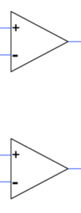
The two comparators compare two of the input voltages to the two values from the resistor ladder, namely, 1/3 * Vcc and 2/3 * Vcc. They output a high value if the voltage on the positive input is greater than the voltage on the negative input.

The top comparator has the negative input connected to 2/3 * Vcc and the positive input connected to the threshold pin. This comparator will out a high value when the threshold is greater than 2/3 * Vcc and a low value at all other times.

The lower comparator has the negative input connected to 1/3 * Vcc and the positive input connected to the trigger input. This comparator will output a high value when the trigger is less than 1/3 * Vcc and a low value at all other times.

S-R Latch

S-R Latch

S-R Latch

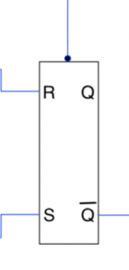
The S-R latch uses the output from the two comparators to determine if the output of the NE555 should be turned on or off. The inverted output from the latch (Q) is connected to the output pin of the NE555 through an invertor.

Q is also connected to the base of the transistor connected to the discharge pin.

Discharge Circuit

Discharge Circuit

Discharge Circuit

The discharge pin is connected to ground through a transistor. The base of the transistor is connected to the inverted output of the S-R latch. So the discharge pin is connected to ground when the S-R latch is in the reset state.

So How Does it Work?

An astable circuit can be used to understand how the various components of the NE555 work together and it is this circuit we will examine next.

Astable Circuit

One of the circuits that can be constructed using the NE555 is a low frequency PWM circuit, known in NE555 parlance as an astable circuit. This can be used in a wide variety of applications from flashing LEDs to the provision of a low frequency clock signal for a digital circuit.

An simple astable circuit can be constructed using two resistors, a capacitor and the NE555 chip. Using the above logical diagram as a starting point we would connect the additional components as follows:

Astable Logical Layout

Astable Logical Layout

The reset pin should be connected to Vcc and the control pin should be connected to ground through a 100nF or 10nF capacitor.

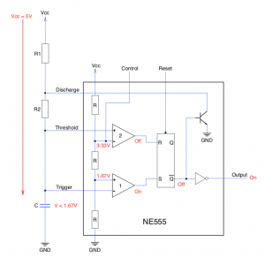
The operation of the astable circuit will be consider by progressing through time from the point that power is applied to the circuit. It is assumed that Vcc is equal to 5V. The makes the nominal values for 1/3 * Vcc = 1.67V and 2/3 * Vcc = 3.3V.

Power On

Capacitor starts to charge

Capacitor starts to charge

At the point where the chip starts the resistor network inside the NE555 will split Vcc into two as noted above. These will appear on the two comparators negative (for comparator 1) and positive (for comparator 2) inputs.

At the same time, the capacitor C will be charged through resistors R1 and R2. At the point shortly after power up there will be very little charge on the capacitor, for argument, let us say that this is 0V. This will place 0V on both the trigger and threshold pins of the NE555.

Comparator 1 will compare the voltage on the trigger pin (negative input) to 1.67V (positive input). As 0V is less than 1.67V this will result in a high output from comparator 1. This high output is applied to the set pin of the S-R latch. Following this through, this will turn the Q output on and the inverted Q output off.

Q output drives both base of the transistor connected to the discharge pin, turning the transistor off and the output pin through the invertor, turning the output on.

Comparator 2 is comparing positive input connected to the charge on the capacitor (currently 0V) to 3.3V. Following this through as we did with comparator 1, 0V is not grester than 3.3V and so comparator 2 outputs a low signal. The low signal on the reset input in the S-R latch has no effect on the output from the S-R latch.

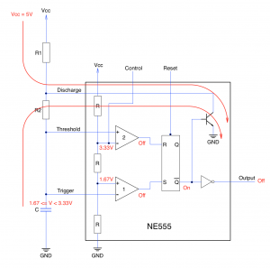
So shortly after power on, comparator 1 has turned the output of the NE555 on and capacitor C is charging. The various parts of the circuit have the inputs and outputs set to the values in the diagram above marked in red.

Capacitor Charge Reaches 1.67V

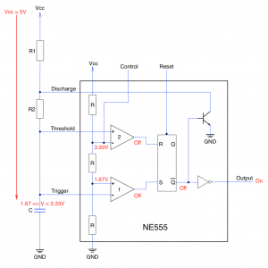
As time progresses, the charge on the capacitor will reach and then exceed 1.67V. The circuit will look like the following:

Capacitor continues to charge

Capacitor continues to charge

At this point a change will occur to comparator 1. The negative input voltage (from the trigger pin) will reach 1.67V. The voltage on the negative input to the comparator will no longer be greater than 1.67V and so the output of the comparator will change from high (on) to low (off). The low signal applied to the set input of the S-R latch will have no effect on the S-R latch (both set and reset inputs to the S-R latch are now low and so the previous state is remembered).

At this point there is no change to the output of the circuit, the output is still latched on and charge continues to build up on the capacitor.

Capacitor Charge Reaches 3.33V

Eventually the charge on the capacitor will reach and exceed 3.33V. This will change the circuit to the following state:

Capacitor starts to discharge

Capacitor starts to discharge

There will be no change to the output of comparator 1 as the voltage applied to the negative input of the comparator remains greater than 1.67V just as it was in the above stage.

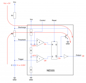
The main change is triggered by comparator 2. The charge on the capacitor is applied to the positive input to the comparator which is now greater than or equal to the 3.33V (from the resistor ladder) applied to the negative input. This causes the comparator to set the output high.

A high output on comparator 2 is applied to the reset input of the S-R latch. This turns the set output (Q) of the latch off and the inverted output (Q) on.

Two things happen when Q is turned on:

  1. The output of the NE555 is turned off
  2. The transistor connected to the discharge pin is turned on

Turning the transistor on changes the flow of current through the circuit. So far current has been flowing through the two resistors, R1 and R2 to charge the capacitor, C. Now the current starts to flow from Vcc to ground through R1.

Current will now also start to flow from the capacitor, through R2 and the transistor to ground. At some point the charge on the capacitor will drop below 3.33V. This will be reflected on the threshold pin connected to comparator 2 and the output of this comparator will be turned off:

Middle of Capacitor Discharging

Middle of Capacitor Discharging

The output of the S-R latch will continue to hold the last state until and hence the output remains off until a signal is applied to the set pin of the S-R latch and so current continues to flow through the transistor.

Capacitor Charge Drops Below 1.67V

At some point the charge on the capacitor will drop below 1.67V and comparator 1 turns on and so Q is turned off once more. The circuit starts to behave as though the system has just been powered on with one slight difference, the charge on the capacitor C starts at 1.67V instead of 0V. The whole cycle of charging and discharging repeats continuously.

Circuit Output

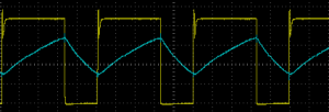
Building the circuit on breadboard and then connecting up an oscilloscope to the discharge and output pin shows the following trace:

Oscilloscope Trace

Oscilloscope Trace

The output is shown in yellow and the discharge is shown in blue.

It is clear to see the charging and discharging of the capacitor coincides with the change in the output state of the NE555.

Timing Calculations

The timing calculations given in the data sheet for the NE555 are as follows.

Note that in the following calculations, resistance is expressed on Ohms, capacitance in Farads and time in seconds.

Charge Time

The charge time depends upon the capacitor and the two resistors R1 and R2 as current flows through the two resistors to charge the capacitor. The time taken to charge is given as:

tcharge = 0.693 * (R1 + R2) * C

Discharge Time

The discharge time is only dependent upon the capacitor and R2 as current does not flow through R1 when the circuit is discharging. the time take to discharge is given as:

tdischarge = 0.693 * R2 * C

Period

The period is the sum of the two timings tcharge and tdischarge. This can be expressed as:

Period = = 0.693 * (R1 + (2 * R2)) * C

The duty cycle and frequency are easily derived from the above.

And Finally…

The NE555 is a versatile chip that can act as more than a simple oscillator. The principles of the above circuit can be used in clock generation, switch debouncing, reset circuits and a whole range of other applications, several of which will be covered in following articles.

Dave Jones (EEVBlog) has put together the Three Fives Timer Kit and has videoed the build process and also provided a run down of the theory of operation referring to the kit schematic. Key times in the video are:

  • 0 – 36 Minutes: Building the kit
  • 36 – 54 Minutes: Examination of the schematic and run through the theory of operation
  • 54 – 62 Minutes: Checking the voltages and output from the kit using an astable circuit

Arithmetic Logic Unit Chip Selection

Sunday, July 16th, 2017

In the previous post, a high level design for an Arithmetic Logic Unit (ALU) was presented. It is time to consider how this could be implemented.

7400 Series Integrated Circuits

The 7400 series of integrated circuits became a staple in computer design and digital electronics in the 1970s and 1980s. These packages implemented everything from simple logic gates (AND, OR, XOR, NOR etc.) through to complex functions such as Error Detection and Correction (see 742960). See this article for a comprehensive list of chips and their functions.

So popular were these chips that they are still available today in the original DIL (Dual In-line Package) as well as surface mount packages.

A number of variations of these ICs were produced:

Series Description
74 Standard TTL
74LS Low-power Schottky
74LAS Advanced Schottky
74ALS Advanced Low-power Schottky

The above list is not comprehensive and many more variations are available.

This series of posts will concentrate on using the LS series of chips where possible.

Internals of the ALU

The ALU in the SSEM needs to support addition (for the JRP instruction) and subtraction (for the SUB and LDN instructions). The previous post presented the internal view of the ALU for the SSEM as:

ALU Internals

Internal view of an Arithmetic Logic Unit showing the control signals and data paths.

The ALU has five distinct components:

  1. Storage for the A and B operands (registers)
  2. Zero Unit
  3. XOR
  4. Adder
  5. ALU Output

Let’s look at how each of these could possibly be implemented using 74LS00 series integrated circuits.

Storage for the A and B operands (registers)

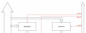
Both of the operands are connected to the data bus at the same time:

Operand A and B

Operand A and B

The Load control signal determines when the input signals should be stored in the register. Each of the registers holding the operand has an independent load signal. So for this part of the ALU a component is required that will:

  1. Take the value on the input pins and store the value
  2. Only load the data into the register when the trigger signal has a known value
  3. Present the stored value on the output pins

The above requirement fits the description of a Flip-Flop (also known as a Latch).

The 74LS00 series has a number of flip-flops and latches available. The 74LS373 contains an octal transparent latch with three state output. This chip is still commonly available and has the following properties:

  1. Input signals can be latched (stored) in the internal registers on request
  2. The output from the latch can be turned on or off, again, on request

The above functions are controlled by two signals:

  1. Clock
  2. Output Enable (~OE)

Clock

When the clock signal is low the inputs are effectively disconnected from the latches. the latches will therefore remain unchanged and hold the previously latched value.

A high clock signal will allow the input pins to the connected to the latches. Any changes on the inputs are presented to the latches. This holds true for as long as the clock signal is in the high state.

The state of the input pins is held in the latches when the clock signal transitions from high to low (on the falling edge of the clock).

Output Enable

The output enable pin is an active low pin (denoted here by the ~ symbol before the name of the pin). This means that the contents of the latches will be output from the chip when the ~OE pin is in the low state.

Putting the ~OE pin in a high state disconnects the latches from the output pins and puts the outputs in a high impedance (also known as a high-Z) state.

Setting ~OE low while the clock pin is high means that the outputs will follow the inputs. This happens because the high clock signal allows the inputs to be connected to the latches and the low output signal puts the value in the latches on to the output pins.

Loading the Latch

From the above description, the Clock pin should be connected to the Load A and Load B signals of the respective operands. This will allow the latch to be loaded with the input signals when the load signal falls from high to low.

The inputs to the chips should be connected to the data bus directly and simultaneously. Data cannot be loaded into the latch until the appropriate load signal transitions from high to low. The load signals will control when the operand changes as follows:

  • Load A (or Load B) signals are low then the inputs will have no impact on the operands. The outputs will reflect the previous value stored in the latch.
  • When Load A (or Load B) is high then the contents of the data bus will be presented to the respective latch. The output of the respective operand will reflect the current contents of the data bus.
  • When the Load A (or Load B) signal falls from high to low, the current contents of the data bus will be stored in the respective operand. The output will reflect this value no matter what happens on the data bus.

Aside: in 2013, the intention was to simulate the SSEM in VHDL. The 74HC373 was simulated in a series of posts around that time.

XOR

The next block available is the 74LS series is the XOR block:

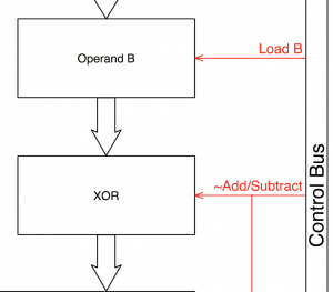
Operand B and XOR

Operand B and XOR

This block performs one part of the negation process allowing the adder to also perform subtraction. The XOR truth table is:

~Add/Subtract Input Value Output
0 0 0
0 1 1
1 0 1
1 1 0

In twos complement, the first part of generating a negative number is to invert the bits in the original number. If you examine the above truth table, when the ~Add/Subtract signal is low, the output reflects the input value. When ~Add/Subtract is high then the output is the inverse of the input value.

~Add/Subtract Operation
0 Add
1 Subtract

So, setting the ~Add/Subtract signal high when the ALU is subtracting operand B from operand A and low when the ALU is adding operand A to operand B will ensure that the correct value is passed through to the adder.

The 74LS86 is a quad 2-input XOR gate (contains four 2-input XOR gates) in a single package. The necessary functionality is achieved by connecting the A inputs (not to be confused with the A operand) of each gate to the ~Add/Subtract signal. All of the A inputs are therefore connected together. The B inputs are connected to the outputs of the B operand latch.

Zero

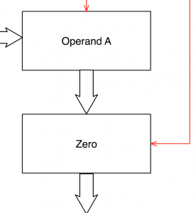
The zero unit sits between the output of the A operand and the Adder. Its function is to select between two possible input values:

  1. Zero
  2. A operand

and pass the selection on to the Adder.

Operand A and Zero

Operand A and Zero

A number of possibilities exist:

  • Use the ~OE signal on the A output to simply turn the output off when zero is required. This may require the use of pull down resistors to prevent a floating signal.
  • Use a buffer chip such as the 74LS245 to connect the Adder to ground when ~OE on the A operand goes high

A little investigation is required.

Adder

The adder unit takes the inputs and simply adds them together:

Adder with inputs.

Adder with inputs.

The 74LS283 is a four bit full adder with carry in and carry out. An 8-bit adder is created by chaining two four bit adders together:

In the case of subtraction, the final part of the negation of a twos complement number is to add 1 to the inverted bit pattern of the original number. Setting the carry in on the first adder effectively adds one to the number. The same ~Add/Subtract signal in the XOR block can be used here as it is low for addition (zero will be added to the sum) and high for subtraction (one will be added to the sum).

ALU Output

The ALU output takes the output of the adder and makes this available to the data bus:

ALU Output

ALU Output

Output to the data bus is controlled by the ALUOutout signal and this function can be performed by a buffer circuit. The 74LS245 is an octal bus transceiver with non-inverting three state outputs. The direction of signal transmission can be controlled using the DIR pin on this chip. In the case of the ALU, the direction is always from the ALU to the data bus and so this pin can be held high (or low) permanently.

Output from 74LS245 is controlled by the ~OE pin. This is an active low pin and the chip is transparent when the signal is low and in high impedance mode when this pin is held high.

Conclusion

All of the integrated circuits for the high level functionality of the ALU have been identified. The next step is to put this together and see if it works as expected.

Something for the next article.

Arithmetic Logic Unit

Monday, June 26th, 2017

The February post regarding the SSEM presented a software implementation of the core hardware:

  • Program counter a.k.a Current Instruction (CI)
  • Arithmetic Logic Unit (ALU)
  • Instruction register a.k.a Present Instruction (PI)
  • Registers (memory)

So, how easy this would be to implement the ALU in 1970s hardware, namely, 74LS series of chips.

Arithmetic Logic Unit

The only explicit arithmetic operation implemented by the ALU is the SUB instruction. There is however, one other operation that requires an arithmetic operation to be performed, the JRP instruction. This instruction adds the contents of a store line to CI and stores the result in CI. The inclusion of an ADD instruction to the ALU instruction set will support the JRP instruction.

Before we progress further it is worth noting that the SSEM uses twos complement representation to store numbers.

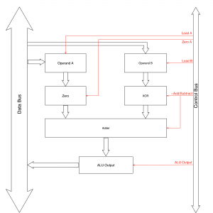
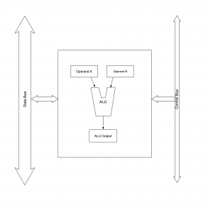
The high level view of the ALU and the way in which it interacts with the other components can be viewed as follows:

High level view of an Arithmetic Logic Unit.

High level view of an Arithmetic Logic Unit.

Two busses run through this CPU:

  1. Data Bus
  2. Control Bus

The Data Bus is used to move data from one part of the CPU to another. This is also connected to the external data bus of the computer allowing the CPU to store and retrieve data from system peripherals and memory.

The Control Bus determines which operations are performed by the CPU (in this particular case, by the ALU) at any point in time.

The ALU uses two input operands (A and B) from the Data Bus. Operations are performed on the two operands, the type of operation is determined by the signals on the Control Bus. The results of the operation are then placed in the ALU Output register. The final step is to make this result available to the Data Bus.

The fact that the SSEM implements only these two arithmetic instructions operating on twos complement numbers leads to a very simple ALU design with very few control signals.

Data Bus

As noted, the data bus moves data around the system. The ALU requires two operands for the ADD or SUB operations. These can be implemented in a single operation or in several stages.

Single Operation

Supplying the data in a single operation would require the data bus to be twice as wide as the word size. In the case of the SSEM this would require a data bus that is 64-bits wide. Operand A would be supplied by one half of the signals on the data bus. Operand B would be supplied by the signals on the other half of the bus.

Multiple Steps

Supplying each operand independently would require a two step process, the first step puts operand A on the data bus and loads into the operand A register. The second step puts operand B on the data bus and loads the data into the operand B register. This is slower, taking two steps, but simplifies the hardware design as a 32-bit data bus is used.

Control Bus

The operation of the CPU is orchestrated by the signals present on the control bus. In the case of the instructions being implemented (ADD and SUB) using two registers the following signals are required:

  1. Load operand A (place the contents on the data bus into operand A)
  2. Load operand B (place the contents on the data bus into operand B)
  3. Output result (place the ALU result onto the data bus)
  4. Add or subtract (Select either addition or subtraction)

There is another instruction that would benefit from having access to the ALU, namely, Load Negative (LDN). This instruction loads a negative number into the accumulator. A negated number can be obtained by subtracting the original number (from a store line) from 0.

If we design the system so that the subtrahend (the number to be subtracted) is always placed in the B operand and operand A can be zero then we can support the LDN instruction. This leads to the final signal, Operand A or Zero.

The full list becomes:

  1. Load operand A (place the contents on the data bus into operand A)
  2. Load operand B (place the contents on the data bus into operand B)
  3. Output result (place the ALU result onto the data bus)
  4. Add or subtract (Select either addition or subtraction)
  5. Operand A or Zero

Inside the ALU

If we add the data paths and control signals to the above diagram we have the following:

ALU Internals

Internal view of an Arithmetic Logic Unit showing the control signals and data paths.

The data paths are shown as broad arrows. The control signals are drawn in red.

Loading the Operand Registers

The data from the data bus is presented to both the A and the B operands at the same time. The data is loaded into the register when the appropriate Load A or Load B signal is set.

Zero Operation

The zero operation is only needed for the A operand. This block will either pass the value in operand A through to the adder (for the SUB, ADD and JRP instruction) or pass 0 through to the adder (for the LDN instruction).

XOR

The XOR block is used to help with the negation of the number in the B operand. In twos complement, a negative number is obtained by inverting the bits in the original number and the adding 1. The XOR helps with the inversion process. Consider the truth table for the XOR operator:

Control Signal Input Value Output
0 0 0
0 1 1
1 0 1
1 1 0

Note that when the Control Signal is 0 then the output from the XOR gate reflects the value on the Input Value. When the Control Signal is 1 then the output is the inverse of the Input Value.

This provides a method for solving the first part of the problem of generating the twos complement negative number, namely, inverting all of the bits in the positive number.

Adder

The adder does exactly what it’s name suggests, it adds two numbers together. Normally, these units have a carry in and a carry out signal to allow multiple units to be chained together:

Two chained four bit adders.

Two chained four bit adders.

When the ~Add/Subtract control signal is set to 0 then the XOR block passes through operand B unchanged. The carry in signal to the first of the adders (Adder-0) is set to 0. The result is that operand A and operand B are added together. This supports the JRP instruction which requires an addition.

When the ~Add/Subtract control signal is set to 1 then the XOR block inverts the bits in operand B. The additional 1 needed for the twos complement process is provided by passing the ~Add/Subtract control signal to the carry in input to the first adder unit (Adder-0 in the above diagram).

Result Output

The final part of the problem is to control when the result from the calculation is output on to the data bus.

Conclusion

A lot of theory, next step is to consider how this can be put into practice.

Something for the next article.

Clocks, Reset Signals and Switch Debouncing

Sunday, February 16th, 2014

Every computer needs a clock circuit to synchronise the operation of the various components. A CPU is no exception. In this post we will create a clock for the CPU. We will also add reset and single step circuits.

The brief for this post is as follows:

  • The reset circuit must be capable of generating both high and low reset signals.
  • A stop/run circuit should allow the CPU to be stopped by the user and the clock single stepped.
  • Internal clock source with a master clock of 4 MHz.
  • Selectable clock frequency which is a fraction (half, quarter etc.) of the master clock source.

Reset Signals

The requirement to have both high and low reset signals is not really too complex as a single inverter can provide this capability. The most complex part of this requirement is to remove the switch bounce from the signal.

Switch De-bouncing

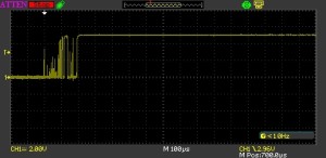
For new readers, switch bounce occurs due to the imperfect nature of mechanical switch. For a brief period of time when a switch is depressed or released there will be a period where the electrical signal is not stable. If you connect an oscilloscope to a switch in an electrical circuit and press the switch you are likely to see traces such as the following:

Switch Bounce

Switch Bounce

The obvious outcome of this is that the circuit can act as though the switch has been pressed multiple times in a short period of time. The answer to the problem is to de-bounce the switch. This removes the additional signals which can be generated. For microcontroller developers there are two possible solutions to this problem, software or hardware de-bouncing. As we have no conventional software environment available to us we must achieve this by hardware de-bouncing.

There are many possible solutions to this problem and you can find some discussions in the following links:

In this circuit there are two switches to debounce, the reset switch and the clock selection switch. The reset switch is a momentary switch and the clock selection switch is a rotary switch. The rotary switch should be viewed as a momentary switch for the purposes of this exercise.

The problem of debouncing the switch can be broken down into two distinct components, namely removing the jitter by rounding off the signal and the squaring off the rounded signal. The jitter can be rounded off by the use of a RC circuit. The above articles suggest that the rounded signal can be squared using an inverter with a Schmitt trigger.

Time to break out the breadboard, oscilloscope and the calculator.

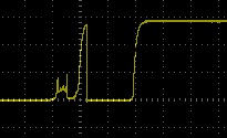
The first thing to examine is the amount of bounce for the switches being used. Hooking up the momentary switch and a resistor resulted in the following traces for the depression of the switch:

Switch Bounce Depression

Switch Bounce Depression

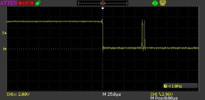
And for the release of the switch:

Switch Bounce Release

Switch Bounce Release

Taking some measurements we see that the maximum bounce appears to be about 5ms for the momentary switch.

Repeating the exercise for the rotary switch reveals that this switch was a lot dirtier. The bouncing continued for about 10ms in the worst case.

Taking the worst case scenario we should assume that the switch is unstable for 10ms and 20ms would allow for an extreme case.

There are two possibilities for debouncing, hardware and software. For a large commercial run where a microcontroller is in use then software debouncing would be used as it requires no additional components. As this is a small run, hardware debouncing is a possibility.

Hardware Debouncing (Circuit 1)

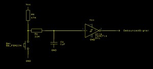
This first hardware debouncer will use an RC network connected to a Schmitt triggered inverter. The basic circuit is:

2RC Debounce

2RC Debounce

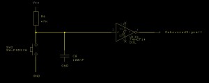
The capacitor C4 charges through R4 and R5. When the capacitor is charged the input to the inverter is high and the output will be low.

Depressing the switch starts the discharge cycle for the capacitor. The capacitor slowly discharges through R4 until it is below the level associated with logic 0 on the inverter. The output of the inverter then goes to logic level 1. The hysteresis of the inverter makes the gate resistant to the time the voltage applied to the input of the inverter is between logic 1 and logic 0. So pressing the switch takes the output high and releasing the switch takes the output from the circuit low.

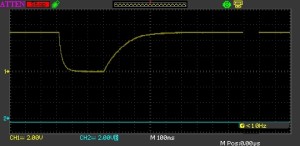
The trick with the circuit above is to select values for R4, R5 and C which eliminate the bounce at both the charge and discharge points in the circuits operation. This circuit gives an output something similar to the following:

RC Added to Switch

RC Added to Switch

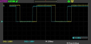
The yellow trace shows the output of the circuit when the oscilloscope probe is connected to the input of the inverter. As you can see, the noisy signal has been replaced by a rapid decay at the start (when the switch is depressed) and a longer rise at the end when the switch is released.

Hardware Debouncing (Circuit 2)

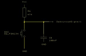
In the last post I was looking at the MSP430. The intention is to look at how it can be used for software debouncing (we’ll come on to that later). The MSP430 Launchpad has a reset button connected to Port 1, pin 3 (P1.3) and this switch is also debounced (the schematics are freely available from TI’s web site). The debounce circuit on the MSP430 looks something like this:

MSP430 Launchpad Debounce Circuit

MSP430 Launchpad Debounce Circuit

Modifying this to add an inverter we get the following:

Modified MSP430 Debounce Circuit

Modified MSP430 Debounce Circuit

The discharge when the button is pressed is a lot quicker but the charging when the button is released show the same characteristics as Hardware Debouncing (Circuit 1). Examining the trace we see that the output from the inverter is good enough for the job at hand.

Software Debouncing

The algorithm for software debouncing is relatively trivial. The microcontroller waits and detects the changing input on of the the pins (say going low to high). Once detected, start a timer and wait for the worst case scenario (we set this to 20ms for the switches being used in this circuit). If at the end of the time period the signal is still high then set the output high, otherwise start the whole process again.

Now this algorithm works well for a single input to a microcontroller but what if you have multiple inputs and outputs all of which need debouncing. This is the scenario with this circuit as the rotary switch allows one selection to be made from a multiple of inputs. In this case the rotary switch acts like multiple switches. Following the above algorithm would require multiple interrupts and timers, many more than found on low end microcontrollers.

Modifying the algorithm to use timers and counters can solve this problem.

  1. Initialise an array of counters (one for each input) to 0
  2. Set the outputs to the same level as the inputs
  3. Setup a timer to trigger on a regular period (say 8ms)
  4. For each input, if the input is different to the output increment the counter for that input, otherwise set the counter to 0
  5. For each counter, if the value has exceeded the threshold count then set the output to the same level as the input

Although this is a little more convoluted it does allow switch debouncing for multiple switches with a simple and cheap microcontroller.

Software Debouncing on the MSP430

The software debouncer will be implemented in MSP430 assembler code developed using IAR Embedded Workbench.

The first thing we need is somewhere to store the counters and some workspace for the application. This application is small and so the registers on the chip should suffice.

;--------------------------------------------------------------------------------------------------
;
;   Switch debouncer for the home made CPU.  This will debounce five switches
;   four through Port 1 and 1 through port 2.
;
;   Copyright (c) Mark Stevens 2014
;
;--------------------------------------------------------------------------------------------------
#include <msp430.h>

;--------------------------------------------------------------------------------------------------
;
;   Global definitions
;
;--------------------------------------------------------------------------------------------------
;
;   Define some symbolic names for the registers holding the counts of the number of interrupts
;   for which the value on the input differs from the output.
;
#define  port0Count r4
#define  port1Count r5
#define  port2Count r6
#define  port3Count r7
;
;   Now some temporary workspace for the Watchdog ISR.
;
#define inputRegister r9
#define temporaryRegister r10
;
INTERRUPT_BASE      equ     0xffe0                  ; Base address of the interrupt vector table.
MAX_COUNTS          equ     4                       ; 4 counts equates to 24ms.

The above defines some symbolic names for the counters and maps these names onto four registers. These are also two registers reserved for workspace for the application.

;--------------------------------------------------------------------------------------------------
;
;   Main program
;
;--------------------------------------------------------------------------------------------------
                    org     0xf800                          ; Program Reset
main                mov     #0x280, SP                      ; Initialize stackpointer
StopWDT             mov.w   #WDT_MDLY_8, &WDTCTL            ; WDT ~8ms interval timer
                    bis.b   #WDTIE, &IE1                    ; Enable WDT interrupt
                    ;
                    ;   Setup the counters.
                    ;
                    mov.w   #0, port0Count
                    mov.w   #0, port1Count
                    mov.w   #0, port2Count
                    mov.w   #0, port3Count
                    ;
                    ;   P1.0, 2, 4, 6 are inputs, P1.1, 3, 5, 7 are outputs.
                    ;
                    bis.b   #0xaa, &P1DIR
                    mov.b   &P1IN, &P1OUT                   ; Start with the outputs equal to the inputs.
                    ;
                    ;   Put the chip to sleep waiting for interupts.  Put it back to sleep
                    ;   if it ever wakes up.
                    ;
Mainloop            bis.w   #CPUOFF + GIE, SR               ; CPU off, enable interrupts
                    jmp     Mainloop

The main program initialises the counters and the ports and turns on the watchdog interrupt (triggered every 8ms – approx). The main program then puts the chip to sleep until the Watchdog interrupt fires.

;--------------------------------------------------------------------------------------------------
;
;   Watchdog interrupt
;
;   Check the input pins (0, 2, 4, 6) and if they are different to the output pins then increment
;   the counter for that pin.
;
;   If the counter reaches MAX_COUNT then transfer the input to the output.
;
;   If the input equals the output then set the counter to 0.
;
;--------------------------------------------------------------------------------------------------
WatchdogISR         mov.b   &P1IN, inputRegister
                    mov.b   &P1OUT, temporaryRegister
                    clrc
                    rrc     temporaryRegister
                    xor.b   temporaryRegister, inputRegister
                    and     #BIT0, inputRegister
                    jz      resetPort0Counter               ; Input bit and output bit are the same.
                    ;
                    ;   Now check the port counters
                    ;
                    inc     port0Count
                    cmp     #MAX_COUNTS, port0Count
                    jne     checkPort2                      ; Not enough differences.
                    ;
                    ;   Transfer the input to the output and reset the counter.
                    ;
                    bit.b   #BIT0, &P1IN
                    jz      resetPort0
                    bis.b   #BIT1, &P1OUT
                    jmp     resetPort0Counter
resetPort0          bic.b   #BIT1, &P1OUT
resetPort0Counter   mov.w   #0, port0Count
checkPort2          ;
                    ;   Checking the remaining ports is left as an exercise for later.
                    ;
                    reti

This is where calculations are performed. Note that the above code only works for one input pin but it can easily be extended to work with four pins. The first thing this routine does is to extract the input and output states of the port. It then works out if there is a difference between the input on P1.0 and the output on P1.1.

The middle block of code increments the counter and checks to see if the counter has reached the threshold. If it hasn’t then we move on to the next port.

The final block of code is executed if the port input/output are different. It transfers the input to the output and then resets the counter.

Deploying this code to the MSP430 and connecting a switch gave the following trace on the oscilloscope:

Switch With Delay

Switch With Delay

As you can see, there is a delay between the switch being depressed and the output being set. The blue trace is wired to the microcontroller input and the yellow trace is the output.

Selecting a debouncer

After many hours working on this circuit I have elected to go with Hardware Debouncing (Circuit 2) with the addition of the Schmitt inverter. This circuit is relatively simple and also meets my long term design goals for this project, namely to use only 1970/80’s technology and using logic gates where possible. It also removes the issue that the MSP430 has a maximum supply voltage of 3.6V and the remainder of this project will be working at 5V.

Selecting the Inverter

Throughout this design process I hit an issue with the inverters I have. I was trying to use the 74LS14 hex Schmitt inverter. For some reason this chip was outputting 1V on the input pin of the logic gate. I could not get the circuits above to work and in the end I ordered some 74HCT14 Schmitt Inverters. Voila, I now have a working debounce circuit.

Something to investigate later…

Reset Circuit

One possibility would be to use the output from the debounced reset switch as a reset signal. This would lead to a variable length reset pulse. Whilst an overly long reset pulse would not be an issue there may be problems if the pulse is too small. This can be solved by using an NE555 timer in monostable mode. The reset signal will still be variable but it will never be shorter than the defined by the components used to control the NE555.

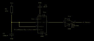
The schematic for the basic monostable NE555 circuit looks as follows:

NE555 Reset Circuit

NE555 Reset Circuit

The length of the pulse is determined by the following formula:

t ~= 1.1RC

In our case R = R3 and C = C2. So this gives:

t ~= 1.1 * R3 * C2>
=> t ~= 1.1 * 45,000 * 100 * 10-9
=> t ~= 4.95ms

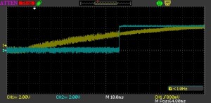
At 4.95ms this might be a little close to the 5ms bounce seen by some of the switches in use. Increasing the values of R3 and C = C2 will increase the duration of the reset pulse. Making R3 = 180K we see the following at the end of the signal:

NE555 End of  Reset Signal

NE555 End of Reset Signal

The full reset pulse looks like this:

NE555 Full Reset Pulse

NE555 Full Reset Pulse

Clock Circuit

The clock for the project can be broken down into two parts:

  • Oscillator
  • Clock Divider
  • Oscillator Circuit

    The oscillator circuit will provide the circuit with the “master clock”. These have been used previously on this blog in the TLC5940 circuit developed a few years ago. In the spirit of reusing old work where possible we will use the basic oscillator circuit from that post here. By changing the 8 MHz resonator for a 4 MHz part we should be able to achieve a 4 MHz master clock signal.

    The schematic for the oscillator can be found below.

    Dividing the Clock

    Dividing the clock circuit by two is easy enough to achieve using a flip-flop. The basic logic diagram is as follows:

    Flip-Flop Divider

    Flip-Flop Divider

    Circuit courtesy of Electronics Tutorials.

    This is easily implemented using the 7474 Dual D-Type Flip-Flops with Preset and Clear.

    The selection of the clock should also be easy if we make the decision that it is invalid to change the clock frequency whilst the system is running. We will rely upon the user to have the discipline not to change the clock in run mode. Since this is an initial design we can look at changing it later.

    This decision means that initially we do not have to worry about glitches due to the clock frequency being changed.

    The selection of the clock frequency can be achieved by feeding all of the clocks into one input of a dual input AND gate. The second input to the gate can then be connected to a rotary switch. The switch will connect the second input to high for the selected frequency. All of the inputs to the other gates will then be grounded. This means that only one gate allows a clock signal through to the system clock signal output.

    We can also use the debounce circuit described above to ensure a smooth transition from one clock to another.

    The schematic for this looks like this:

    Oscillator and Clock Dividers

    Oscillator and Clock Dividers

    By hooking up the logic analyser to the system clock output and the various outputs from the clock divider circuit we see the following:

    Clock and Flip Flop Output

    Clock and Flip Flop Output

    Hooking up the rotary switch to the debounce circuit and the AND gates will allow the selection of the master clock output.

    Conclusion

    The home built CPU is on it’s way. We now have a heart beat (clock) for the circuit and a method for issuing a reset request to the circuit.

    One final refinement would be the addition of a buffer driver chip to the circuit to allow for the fact that the clock and reset signals will be being fed into a larger circuit.