C# SerialPort on the Raspberry Pi
Sunday, May 19th, 2013Sometimes you have to do something just because you can. Today was no exception. Take one Raspberry Pi board (Linux) and give it a dose of .NET loving…
I can hear people screaming NO! but it’s too late, I’ve done it.
To be honest, I’m not the first person to use .NET on the Raspberry Pi. In fact I used this installation guide to install Mono on the Raspberry Pi.
So what interested me? Simply put, hardware interfacing. Could the .NET hardware classes (i.e. SerialPort) be used on the Raspberry Pi? There was only one way to find out.
Raspberry Pi Setup
The first thing to do was to set up the Raspberry Pi using the instructions in the blog mentioned above. This was not difficult although it was time consuming as it took a while to compile.
When this is complete a simple program should demonstrate if the serial ports are available to us. The following code should show this:
namespace ConsoleApplication1
{
	class Program
	{
		public static void Main(string[] args)
		{
			SerialPort sp = new SerialPort("/dev/ttyAMA0", 115200, Parity.None, 8, StopBits.One);
			sp.Open();
			for (int index = 0; index < 10; index++)
			{
				string result = string.Format("{0} Testing", index);
				sp.Write(result);
			}
			sp.Close();
		}
	}
}
As you can see, this code is not too complex. It merely opens a serial port and then starts to output data to the port. The only tricky part of the job was to locate the name to be used for the serial port. It’s been too long since I used Unix in anger.
Testing the Application
Testing is not too complex as the test application is simply outputting a text message. We can see the output by hooking up PuTTY to a serial port on a computer.
The hardware is also simple to hook up. The FTDI cable I have allows me to connect a 3.3V TTL serial device to my PC over USB. This USB device then appears as a standard serial device on the PC. Three connections are required:
| Raspberry Pi | FTDI Cable |
| Ground | Ground |
| Rx | Tx |
| Tx | Rx |
Strictly speaking, we do not have to connect the Tx on the FTDI cable to the Rx on the Raspberry Pi as we will not be transmitting anything from the PC to the Raspberry Pi in this example.
Once the hardware is connected you will need to fire up PuTTY and connect it to the serial port on your PC. Ensure that the settings used match those in the application code above.
Assuming that you now have Mono installed and the application typed in ready to go, type the following commands into a shell on the Raspberry Pi:
mcs serial.cs
mono serial.exe
The first command invokes the Mono C# compiler. The second tells mono to execute the application which has been compiled.
If all has gone well then you will see something like this in the PuTTY window running on the PC:
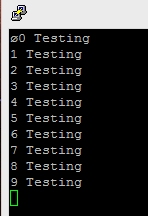
Serial Output in Putty
Conclusion
I was rather interested to see that the C# skills acquired on the PC could also be used on the Raspberry Pi. The only thing missing on the Pi was a good development environment.