Making a Netduino GO! Module – Stage 6 – Assembling the Prototype
Monday, May 6th, 2013A few days ago I received a package from China, namely my Output Expander prototype boards:
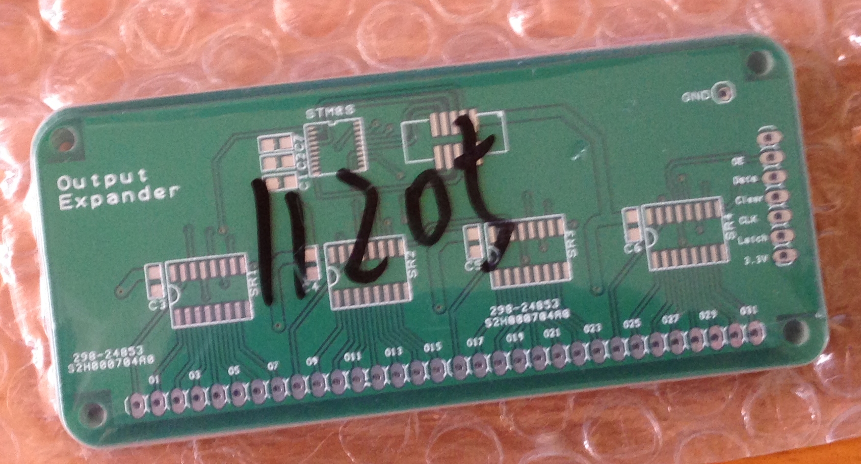
Bubble Wrapped Boards From China
Could not wait to unwrap them:
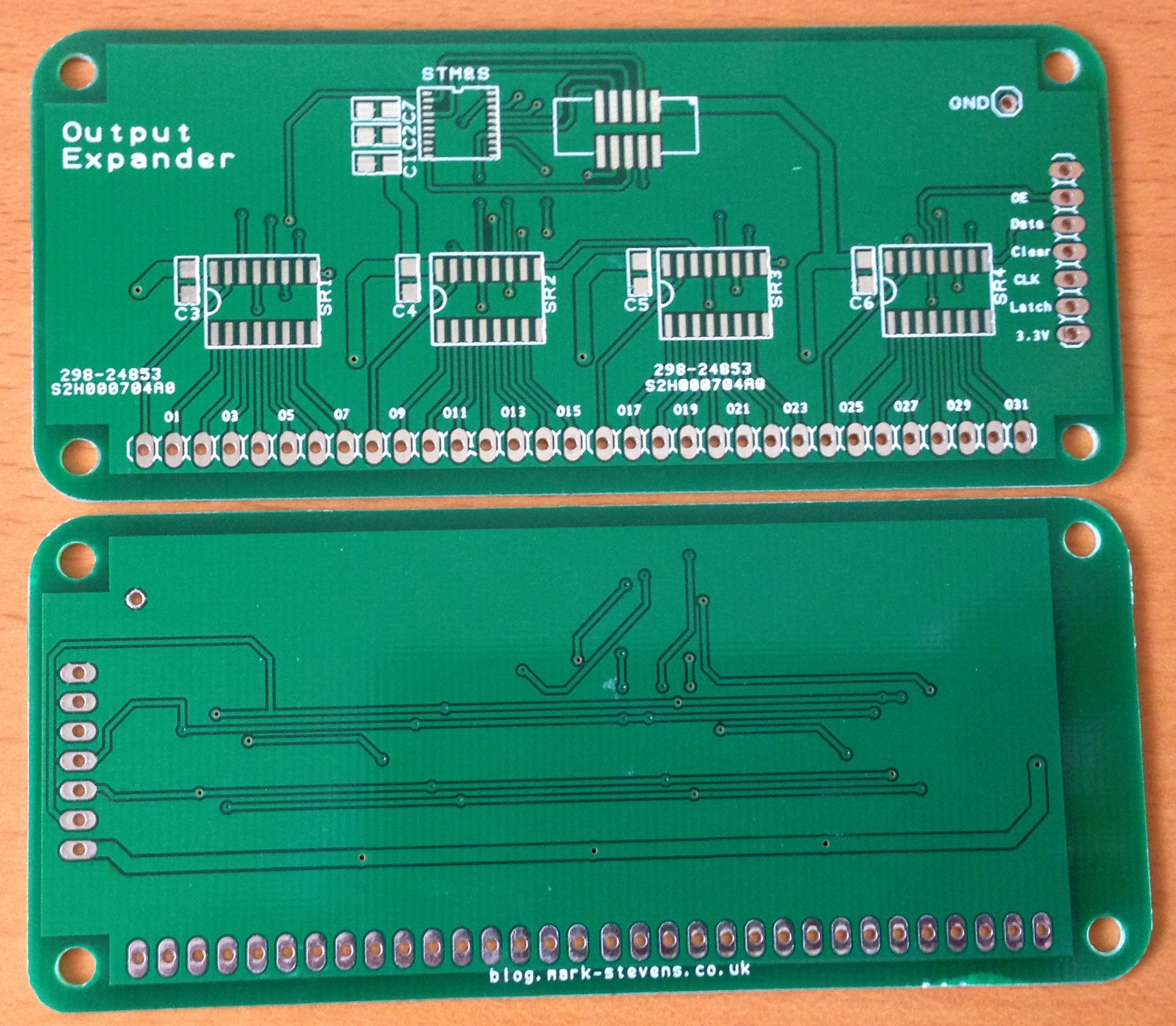
OutputExpander Bare Boards
Only one thing left to do, start assembling them. As with all projects this will be broken down into steps:
- Add the STM8S microcontroller and test
- Add one 74HC595 shift register and test
- Complete the board and add connectors and of course, test
By using a modular approach it should be easy to detect a problem with the design or assembly.
Component List
The board requires the following components:
| Component | Value | Quantity |
| STM8S103F3 | NA | 1 |
| IDC socket | 1.27″ pitch | 1 |
| Sr1, SR2, Sr3, SR4 | SOL / SOP16 | 4 |
| C2 | 1uF | 0403 |
| C1, C3, C4, C5, C6, C7 | 100nF – 0403 | 6 |
| Connectors | 0.1″ | Misc |
When these arrive be prepared, they are small!
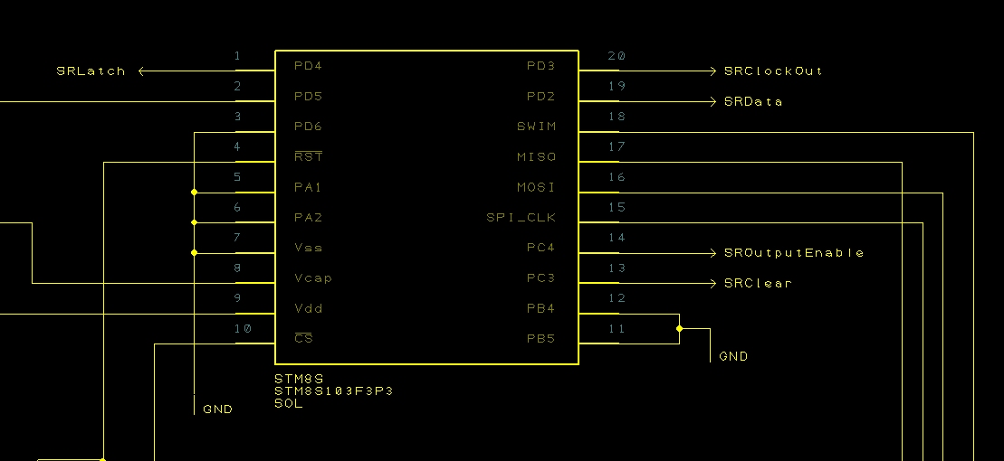
Adding the Microcontroller
The board will need a microcontroller and some way of programming it. The logical first task is to add the controller, socket and the supporting passive components. Doing this will allow us to programme the controller with the firmware. As a test we can connect the programmed board to the Netduino Go!. If the connections between the board and the Netduino GO! are correct then the blue LED on the socket on the Netduino Go! should light.
If you are attempting to follow this series and you are making your own board then I recommend you browse the net and have a look for videos on soldering SMD components. I found the tutorials on drag soldering really useful.
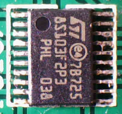
Out with the soldering iron, a magnifier (it was needed). One thing I noticed was the difference between the 74HC595 pads and the pads for the STM8S. The 74HC595 component used was a built in component whilst the STM8S was a component I had created. The most noticeable difference between the two parts was the size of the pads on the PCB compared to the size of the component. The 74HC595 pads were elongated. These make soldering easier.
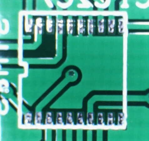 |  |
| STM8S | 75HC595 |
Although the pins on the STM8S are only 0.65mm pitch, soldering is not as difficult as it first appears. A quick first attempt gave the following:
STM8S Mounted On Board
There is only one item of concern and that is the whisker of solder between the fourth and fifth pins down on the right hand side of the image. This was quickly tidied up by dragging the soldering iron between the two pins.
Next task was to add the passives which supported the STM8S leaving the passives for the shift registers for later. This is where you get some idea of the difference between the size of the components vs the size of the tools you are using:

Capacitor and Tools
At this point I realised that an 0403 (metric sizing) component is 0.4mm x 0.3mm and the smallest soldering iron bit I has was about 1.5mm. Not to worry, the pads on the board are a reasonable size, simply tin the pads and then slide the capacitor into the molten solder.
The next job was to add the socket for the GoBus. The sockets are surface mounted 1.27″ pitch IDC sockets. I found the easiest way to add these was to tin one pad and then slide the socket into place. The remaining pads could be soldered by placing the solder at the end of the connector and then applying heat and letting the solder run under the socket. It’s not as difficult as it sounds.
At this point, the microcontroller should be in place with enough supporting hardware to allow it to be programmed. This was achieved by connecting the ST-Link/V2 programmer to the prototype board using the Komodex Breakout Board. The firmware developed in the previous posts was loaded into the development environment and deployed top the microcontroller.
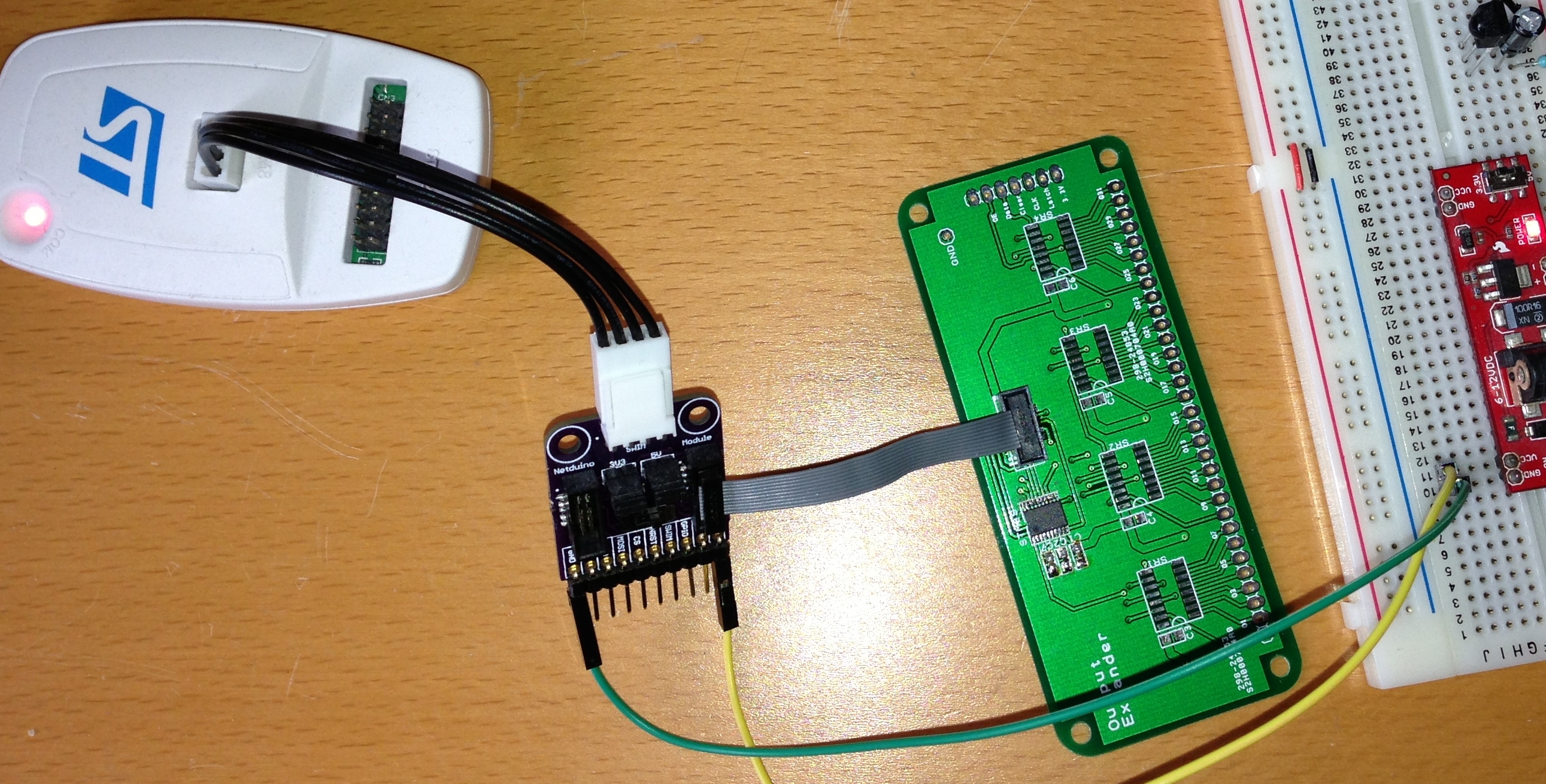
Programming the STM8S
No deployment errors!
A good indication that the microcontroller and the supporting hardware are functioning correctly.
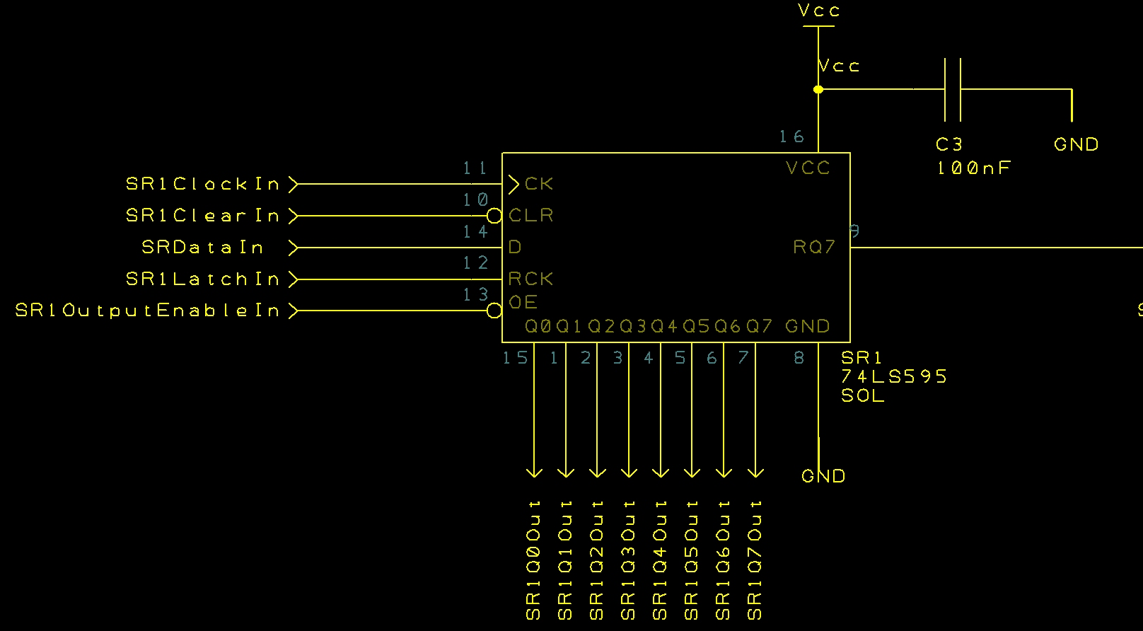
Add a Shift Register
Next step is to add a single shift register and see if we get some output. Soldering the shift registers was a lot simpler than the STM8S as the pin pitch was greater. These could be soldered more conventionally although the pitch was finer than you may be used to if you have only worked with PTH components.
Connecting the module to the Netduino GO! acts as a quick check:

Netduino Go! Connected to OutputExpander
The blue LED lights up – the Netduino GO! recognises the OutputExpander as a valid module.
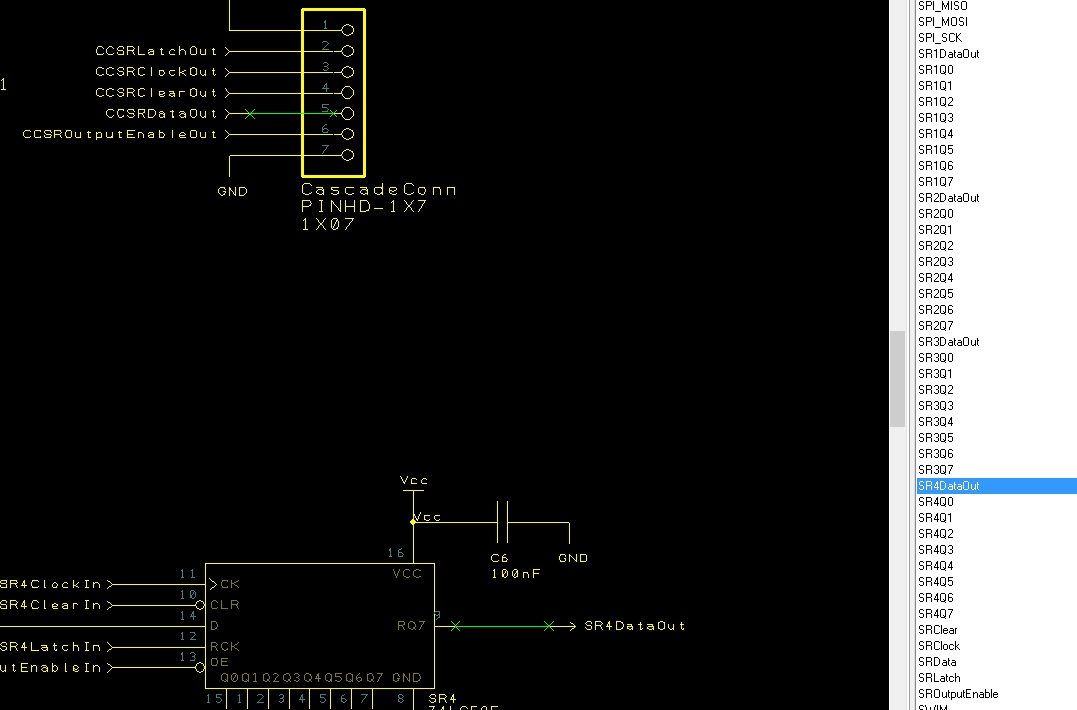
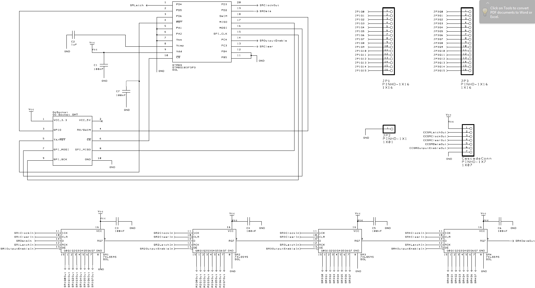
Adding the single register worked and so the next task is to add the remaining registers and connectors.
But All Was Not Well…
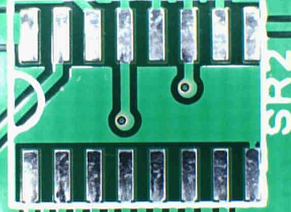
During the assembly and testing process I had managed to accidentally short a few pins on the shift registers. This resulted in no output from the OutputExpander module. Breaking out the scope and the logic analyser proved that something was very wrong. The following trace shows the problem:

Original Output From the OutputExpander
It appears that the latch and clear lines were being triggered at the same time. I was able to establish by disconnecting the module from the circuit that there was not short between the two lines. Something else must be going on. Some further digging into the output from the logic analyser showed that the clear signal was being triggered slightly before the latch signal and that the latch was being released slightly after the clear signal. As a result I would expect no output from the shift registers – this is what I was seeing.
Not wanting to waste money on components I continued to check the circuit but could not find anything else obviously wrong with the soldering or the software.
Only one remaining option. Try a putting together a new board. Back to step one.
A New Board
Building the new board was a lot quicker than the first. Following the same procedure (one step at a time and test all the way) produced a new board:
Before testing the board there was a final modification to make. This time to the software. The board has the outputs labelled from left to right with the lower bits being to the right of the board. The prototype module had the shift registers ordered from right to left. A quick change to the C code on the STM8S soon resolved this problem:
//--------------------------------------------------------------------------------
//
//  GO! function 2 - Output the specified bytes to the shift registers.
//  Tx buffer.
//
void SetShiftRegisters()
{
    for (int index = 0; index < _numberOfShiftRegisters; index++)
    {
        _registers[index] = _rxBuffer[5 - index];
    }
    OutputData();
    NotifyGOBoard();
}
A small bug had also been noticed in the clock configuration method. The code stated that CCO was turned off but the code actually turned it on. The code should read:
//--------------------------------------------------------------------------------
//
//  Setup the system clock to run at 16MHz using the internal oscillator.
//
void InitialiseSystemClock()
{
    CLK_ICKR = 0;                       //  Reset the Internal Clock Register.
    CLK_ICKR_HSIEN = 1;                 //  Enable the HSI.
    CLK_ECKR = 0;                       //  Disable the external clock.
    while (CLK_ICKR_HSIRDY == 0);       //  Wait for the HSI to be ready for use.
    CLK_CKDIVR = 0;                     //  Ensure the clocks are running at full speed.
    CLK_PCKENR1 = 0xff;                 //  Enable all peripheral clocks.
    CLK_PCKENR2 = 0xff;                 //  Ditto.
    CLK_CCOR = 0;                       //  Turn off CCO.
    CLK_HSITRIMR = 0;                   //  Turn off any HSIU trimming.
    CLK_SWIMCCR = 0;                    //  Set SWIM to run at clock / 2.
    CLK_SWR = 0xe1;                     //  Use HSI as the clock source.
    CLK_SWCR = 0;                       //  Reset the clock switch control register.
    CLK_SWCR_SWEN = 1;                  //  Enable switching.
    while (CLK_SWCR_SWBSY != 0);        //  Pause while the clock switch is busy.
}
Testing
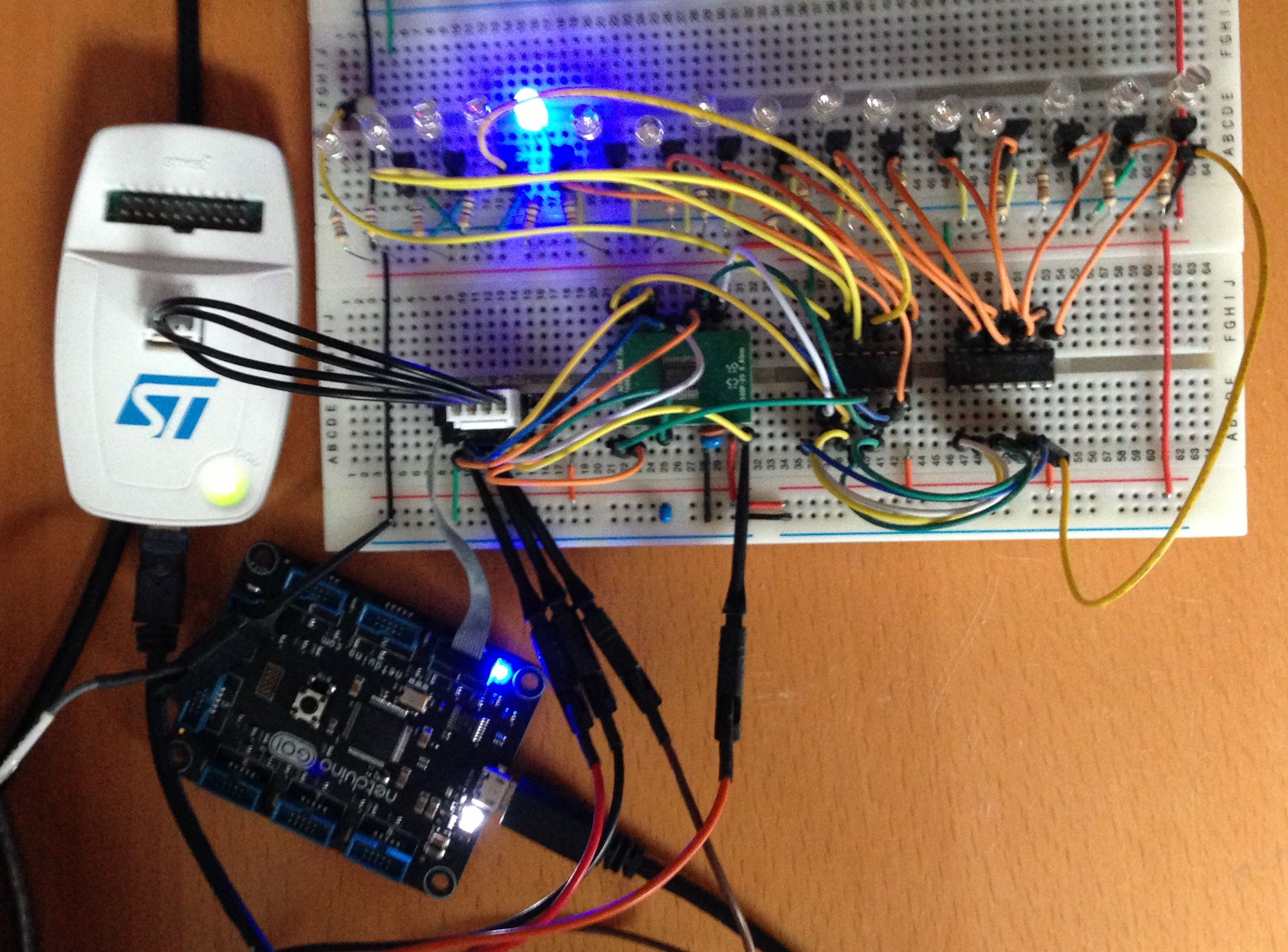
The step by step testing process had shown that a single shift register worked, now to prove that four worked. Now it was time to add some more and connect some LEDs:

Netduino Go OutputExpander and Some LEDs
And here’s a video of it working:
Conclusion
Assembly was not as difficult as it first appears even considering the small size of the components. In fact the STM8S was programmed first time.
One piece of equipment I did find invaluable was a cheap USB microscope. These don’t give a high resolution image but they do allow you to zoom in on the board and check for problems.
One final post left – time to reflect on the process.