Having succeeded at getting a basic I2C master working on the STM8S it is not time to start to look at I2C slave devices on the STM8S.
The project will be a simple one, the STM8S will take a stream of bytes and perform simple addition. When requested, the STM8S will return the total as a 16-bit integer. Each new write request will clear the current total and start the whole process again.
Simple enough so let’s get started.
This post is a fairly long as it contains a lot of code so it might be a good time to grab a beer and settle down.
Simple Slave Adder
The slave adder is a simple device running over I2C. The devices has the following properties:
- Acts as an I2C slave device with address 0x50
- I2C bus speed is 50 KHz
- Upon receiving a valid start condition and address for a write operation the device will clear the current total.
- Bytes written to the device will be summed and a running total kept.
- A start condition with a valid address for a read operation will return the current total as a 16-bit integer, MSB first.
A Netduino 3 will be used as the I2C bus master device. This runs the .NET Microframework and has an implementation of the I2C protocol built into the framework. This gives a good reference point for the master device i.e. someone else has debugged that so we can assume that the device is working as per the protocol specification.
As mentioned in the previous article on I2C Master devices, there is a really good article about the I2C protocol on Wikipedia. If you want more information about the protocol then I suggest you head over there.
Netduino Code
The initial version of the I2C master device will simply send two bytes of data for the I2C slave device to sum. The code is simple enough:
using Microsoft.SPOT;
using Microsoft.SPOT.Hardware;
using System.Threading;

namespace I2CMaster
{
    public class Program
    {
        public static void Main()
        {
            //
            //  Create a new I2C object on address 0x50 with the clock running at 50 KHz.
            //
            I2CDevice i2cBus = new I2CDevice(new I2CDevice.Configuration(0x50, 50));
            //
            //  Create a transaction to write two bytes of data to the I2C bus.
            //
            byte[] buffer = { 1, 2 };
            I2CDevice.I2CTransaction[] transactions = new I2CDevice.I2CTransaction[1];
            transactions[0] = I2CDevice.CreateWriteTransaction(buffer);
            while (true)
            {
                int bytesRead = i2cBus.Execute(transactions, 100);
                Thread.Sleep(1000);
            }
        }
    }
}
The above application creates a new instance of the I2CDevice with a device address of )x50 and a clock frequency of 50 KHz. A single transaction is created and the master writes the same two bytes to the I2C bus every second.
STM8S Code
As with the I2C Master article, much of the action happens in two places:
- I2C device initialisation method
- I2C Interrupt Service Routine (ISR)
The initialisation method sets up the I2C peripheral on the STM8S and enters the waiting state, waiting for the master to put data onto the I2C bus.
The ISR will deal with the actual data processing and in a full application it will also deal with any error conditions that may arise.
I2C Initialisation
The initialisation method sets up the I2C bus by performing the following tasks:
- Setting the expected clock frequency
- Setting the device address
- Turning the interrupts on
The I2C peripheral must be disabled before configuring certain aspects of the peripheral, namely clock speeds:
The peripheral needs to know the current master clock frequency, the I2C mode (Standard or Fast) and the clock divider values. These must all be configured whilst the peripheral is disabled.
I2C_FREQR = 16;                     //  Set the internal clock frequency (MHz).
I2C_CCRH_F_S = 0;                   //  I2C running is standard mode.
I2C_CCRL = 0xa0;                    //  SCL clock speed is 50 KHz.
I2C_CCRH_CCR = 0x00;
The device assumes that we will be using the standard 16 MHz clock speed which has been used in the other tutorials in this series. This is indicated by the I2C_FREQR register.
The values for the clock control register (I2C_CCRL and I2C_CCRH_CCR were simply taken from the STM8S programming reference manual. There is no coincidence that a bus speed of 50 KHz was chose, it is simply one of the reference values in the table. No point in creating work if you do not have to. If you want different speeds then you can either use one of the defined values in the remainder of the table or use the formulae provided.
The next step is to define the device address and addressing mode. I2C allows both 7 and 10 bit addressing modes. For simplicity this device will use a 7-bit device address:
I2C_OARH_ADDMODE = 0;               //  7 bit address mode.
I2C_OARH_ADD = 0;                   //  Set this device address to be 0x50.
I2C_OARL_ADD = 0x50;
I2C_OARH_ADDCONF = 1;               //  Docs say this must always be 1.
The device also allows for the maximum rise time to be configured. This example uses 17uS as the maximum time:
The I2C peripheral allows for three different interrupt conditions to be defined, buffer interrupts, event interrupts (start condition etc.) and error interrupts. For convenience we will turn all of these on:
I2C_ITR_ITBUFEN = 1;                //  Buffer interrupt enabled.
I2C_ITR_ITEVTEN = 1;                //  Event interrupt enabled.
I2C_ITR_ITERREN = 1;
Now that the peripheral is configured we need to re-enable it:
The last bit of initialisation is to configure the device to return an ACK after each byte:
At this point the I2C peripheral should be listening to the I2C bus for a start condition and the address 0x50.
I2C Interrupt Service Routine (ISR)
The ISR contains the code which processes the data and error conditions for the I2C peripheral. All of the I2C events share the same ISR and the ISR will need to interrogate the status registers in order to determine the exact reason for the interrupt.
Starting with an empty ISR we have the following code:
#pragma vector = I2C_RXNE_vector
__interrupt void I2C_IRQHandler()
{
}
There are several other vector names we could have chosen, they all contain the same value and the value I2C_RXNE_vector was chosen arbitrarily.
Assuming that there are no errors on the bus, the I2C master code above will cause the following events to be generated:
- Address detection
- Receive buffer not empty
This initial simple implementation can use these two events to clear the total when a new Start condition is received and add the current byte to the total when data is received.
if (I2C_SR1_ADDR)
{
    //
    //  In master mode, the address has been sent to the slave.
    //  Clear the status registers and wait for some data from the salve.
    //
    reg = I2C_SR1;
    reg = I2C_SR3;
    _total = 0;                 // New addition so clear the total.
    return;
}
I2C_SR1_ADDR should be set when an address is detected on the bus which matches the address currently in the address registers. As a starter application the code can simply assume that any address is going to be a write condition. The code can clear the totals and get ready to receive data. Note that this will be expanded later to take into consideration the fact that the master can perform both read and write operations.
The next event we need to consider is the receipt of data from the master. This will trigger the Receive Buffer Not Empty interrupt. This simple application should just read the buffer and add the current byte to the running total:
if (I2C_SR1_RXNE)
{
    //
    //  Received a new byte of data so add to the running total.
    //
    _total += I2C_DR;
    return;
}
As indicated earlier, the I2C ISR is a generic ISRT and is triggered for all I2C events. The initialisation code above has turned on the error interrupts as well as the data capture interrupts. Whilst none of the code in this article will handle error conditions, the ISR will output the status registers for diagnostic purposes:
PIN_ERROR = 1;
__no_operation();
PIN_ERROR = 0;
reg = I2C_SR1;
BitBang(reg);
reg = I2C_SR3;
BitBang(reg);
This will of course require suitable definitions and support methods.
Putting this all together gives an initial implementation of a slave device as:
//
//  This application demonstrates the principles behind developing an
//  I2C slave device on the STM8S microcontroller.  The application
//  will total the byte values written to it and then send the total
//  to the master when the device is read.
//
//  This software is provided under the CC BY-SA 3.0 licence.  A
//  copy of this licence can be found at:
//
//  http://creativecommons.org/licenses/by-sa/3.0/legalcode
//
#if defined DISCOVERY
    #include <iostm8S105c6.h>
#else
    #include <iostm8s103f3.h>
#endif
#include <intrinsics.h>

//
//  Define some pins to output diagnostic data.
//
#define PIN_BIT_BANG_DATA       PD_ODR_ODR4
#define PIN_BIT_BANG_CLOCK      PD_ODR_ODR5
#define PIN_ERROR               PD_ODR_ODR6

//
//  Somewhere to hold the sum.
//
int _total;

//
//  Bit bang data on the diagnostic pins.
//
void BitBang(unsigned char byte)
{
    for (short bit = 7; bit >= 0; bit--)
    {
        if (byte & (1 << bit))
        {
            PIN_BIT_BANG_DATA = 1;
        }
        else
        {
            PIN_BIT_BANG_DATA = 0;
        }
        PIN_BIT_BANG_CLOCK = 1;
        __no_operation();
        PIN_BIT_BANG_CLOCK = 0;
    }
    PIN_BIT_BANG_DATA = 0;
}

//
//  Set up the system clock to run at 16MHz using the internal oscillator.
//
void InitialiseSystemClock()
{
    CLK_ICKR = 0;                       //  Reset the Internal Clock Register.
    CLK_ICKR_HSIEN = 1;                 //  Enable the HSI.
    CLK_ECKR = 0;                       //  Disable the external clock.
    while (CLK_ICKR_HSIRDY == 0);       //  Wait for the HSI to be ready for use.
    CLK_CKDIVR = 0;                     //  Ensure the clocks are running at full speed.
    CLK_PCKENR1 = 0xff;                 //  Enable all peripheral clocks.
    CLK_PCKENR2 = 0xff;                 //  Ditto.
    CLK_CCOR = 0;                       //  Turn off CCO.
    CLK_HSITRIMR = 0;                   //  Turn off any HSIU trimming.
    CLK_SWIMCCR = 0;                    //  Set SWIM to run at clock / 2.
    CLK_SWR = 0xe1;                     //  Use HSI as the clock source.
    CLK_SWCR = 0;                       //  Reset the clock switch control register.
    CLK_SWCR_SWEN = 1;                  //  Enable switching.
    while (CLK_SWCR_SWBSY != 0);        //  Pause while the clock switch is busy.
}

//
//  Initialise the I2C system.
//
void InitialiseI2C()
{
    I2C_CR1_PE = 0;                     //  Disable I2C before configuration starts.
    //
    //  Set up the clock information.
    //
    I2C_FREQR = 16;                     //  Set the internal clock frequency (MHz).
    I2C_CCRH_F_S = 0;                   //  I2C running is standard mode.
    I2C_CCRL = 0xa0;                    //  SCL clock speed is 50 KHz.
    I2C_CCRH_CCR = 0x00;
    //
    //  Set the address of this device.
    //
    I2C_OARH_ADDMODE = 0;               //  7 bit address mode.
    I2C_OARH_ADD = 0;                   //  Set this device address to be 0x50.
    I2C_OARL_ADD = 0x50;
    I2C_OARH_ADDCONF = 1;               //  Docs say this must always be 1.
    //
    //  Set up the bus characteristics.
    //
    I2C_TRISER = 17;
    //
    //  Turn on the interrupts.
    //
    I2C_ITR_ITBUFEN = 1;                //  Buffer interrupt enabled.
    I2C_ITR_ITEVTEN = 1;                //  Event interrupt enabled.
    I2C_ITR_ITERREN = 1;
    //
    //  Configuration complete so turn the peripheral on.
    //
    I2C_CR1_PE = 1;
    //
    //  Acknowledge each byte with an ACK signal.
    //
    I2C_CR2_ACK = 1;
}

//
//  I2C interrupts all share the same handler.
//
#pragma vector = I2C_RXNE_vector
__interrupt void I2C_IRQHandler()
{
    unsigned char reg;

    if (I2C_SR1_ADDR)
    {
        //
        //  Clear the status registers and wait for some data from the salve.
        //
        reg = I2C_SR1;
        reg = I2C_SR3;
        _total = 0;                 // New addition so clear the total.
        return;
    }
    if (I2C_SR1_RXNE)
    {
        //
        //  Received a new byte of data so add to the running total.
        //
        _total += I2C_DR;
        return;
    }
    //
    //  Send a diagnostic signal to indicate we have cleared
    //  the error condition.
    //
    PIN_ERROR = 1;
    __no_operation();
    PIN_ERROR = 0;
    //
    //  If we get here then we have an error so clear
    //  the error, output the status registers and continue.
    //
    reg = I2C_SR1;
    BitBang(reg);
    reg = I2C_SR3;
    BitBang(reg);
}

//
//  Main program loop.
//
int main()
{
    _total = 0;
    __disable_interrupt();
    //
    //  Initialise Port D.
    //
    PD_ODR = 0;             //  All pins are turned off.
    PD_DDR_DDR4 = 1;        //  Port D, bit 4 is output.
    PD_CR1_C14 = 1;         //  Pin is set to Push-Pull mode.
    PD_CR2_C24 = 1;         //  Pin can run up to 10 MHz.
    //
    PD_DDR_DDR5 = 1;        //  Port D, bit 5 is output.
    PD_CR1_C15 = 1;         //  Pin is set to Push-Pull mode.
    PD_CR2_C25 = 1;         //  Pin can run up to 10 MHz.
    //
    PD_DDR_DDR6 = 1;        //  Port D, bit 6 is output.
    PD_CR1_C16 = 1;         //  Pin is set to Push-Pull mode.
    PD_CR2_C26 = 1;         //  Pin can run up to 10 MHz.
    //
    InitialiseSystemClock();
    InitialiseI2C();
    __enable_interrupt();
    while (1)
    {
        __wait_for_interrupt();
    }
}
Executing the Applications
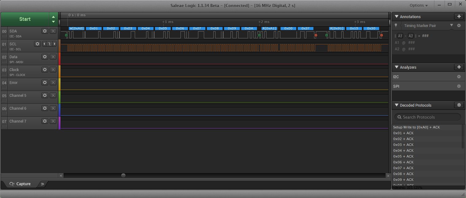
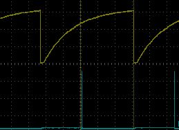
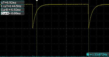
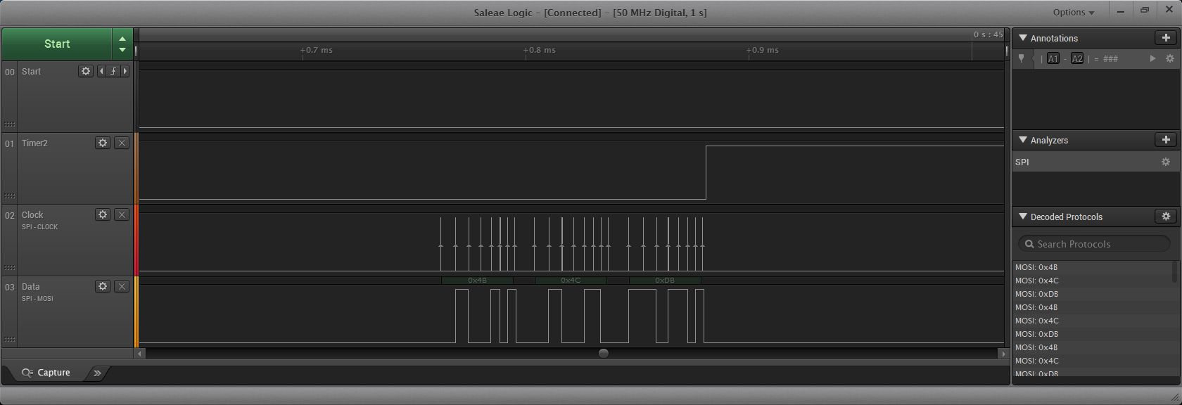
At this stage a quick test with the two devices connected and the logic analyser will show the master device outputting data to the I2C bus. The correct operation of the I2C salve device can be verified by setting break points with in the two if statements in the ISR. Note that this will generate some errors but it is good enough to verify that the ISRs are being triggered correctly.

STM8 I2C Write Condition
The above shows the output from the Saleae Logic Analyser when the write transaction is sent to the bus by the Netduino.
Reading and Writing with I2C Slaves
At this point the above code should be accepting data from the Netduino 3. It is now time to expand the code to take into account the requirement to read back data from the slave device.
Netduino Code
The Netduino code will need to be modified to generate both a write transaction to send data to the I2C slave device and a read transaction to retrieve the results from the calculation.
using Microsoft.SPOT;
using Microsoft.SPOT.Hardware;
using System.Threading;

namespace I2CMaster
{
    public class Program
    {
        public static void Main()
        {
            //
            //  Create a new I2C object on address 0x50 with the clock running at 50 KHz.
            //
            I2CDevice i2cBus = new I2CDevice(new I2CDevice.Configuration(0x50, 50));
            //
            //  Create a transaction to write two bytes of data to the I2C bus.
            //
            byte[] buffer = { 1, 2, 3, 4, 5, 6, 7, 8, 9, 10 };
            byte[] resultBuffer = new byte[2];
            I2CDevice.I2CTransaction[] transactions = new I2CDevice.I2CTransaction[2];
            transactions[0] = I2CDevice.CreateWriteTransaction(buffer);
            transactions[1] = I2CDevice.CreateReadTransaction(resultBuffer);
            while (true)
            {
                int bytesRead = i2cBus.Execute(transactions, 100);
                Thread.Sleep(1000);
            }
        }
    }
}
The transaction array has been expanded to contain a second transaction to read the data from the device. The data to be summed has also been expanded to include a further eight elements.
STM8S Code
A state machine will be used to allow the STM8S to work out what action should be taken within the ISR. This is required as the i”c peripheral will generate an event for the address detection for both the write transaction and the read transaction. The application will need to be able to differentiate between the two conditions as one requires the total to be cleared, the other requires that the total is sent back to the master device.
The state machine contains the following states:
- Waiting for a write condition to start
- Adding data to the running total
- Sending the MSB of the total
- Sending the LSB of the total
This is represented in code by an enum and a global variable:
typedef enum
{
    ISWaiting,                    //  Waiting for comms to start.
    ISAdding,                     //  Adding bytes of data.
    ISSendingMSB,                 //  Sending MSB of total.
    ISSendingLSB                  //  Sending LSB of total.
} I2CStateType;
I2CStateType _i2cState;
The ISR will need to be changed in order to deal with the state machine and also handle the slave transmitting data to the master device. The first change is to the address detection. This assumes that the main program loop initialises the state to ISWaiting:
if (I2C_SR1_ADDR)
{
    //
    //  Slave address received, work out if to expect a read or a write.
    //
    if (_i2cState == ISWaiting)
    {
        _i2cState = ISAdding;
        _total = 0;             // New addition so clear the total.
    }
    reg = I2C_SR1;
    reg = I2C_SR3;
    return;
}
The code above works out if the application is waiting for the first write condition (IsWaiting) or if the address detection has been triggered by a read condition (any other state).
Next, any other data reception is assumed to be data to be added to the total. The state is changed to IsAdding just in case:
if (I2C_SR1_RXNE)
{
    //
    //  Receiving data from the master so we must be adding.
    //
    _total += I2C_DR;
    _i2cState = ISAdding;
    return;
}
Next we have two new conditions we have not considered so far, the first is the fact that we need to transmit the result to the master. The request from the client will trigger a Transmit Buffer Empty event:
if (I2C_SR1_TXE)
{
    if (_i2cState == ISAdding)
    {
        I2C_DR = (_total >> 8) & 0xff;
        _i2cState = ISSendingMSB;
    }
    else
    {
        I2C_DR = _total & 0xff;
        _i2cState = ISSendingLSB;
    }
    return;
}
The master is asking for two bytes and the application needs to track if we are transmitting the most significant byte (MSB) or least significant byte (LSB).
The next new condition is the acknowledge event. This is generated at the end of the master read operation. This will set the system back into a waiting condition:
if (I2C_SR2_AF)
{
    I2C_SR2_AF = 0;             //  End of slave transmission.
    _i2cState = ISWaiting;
    return;
}
The full application becomes:
//
//  This application demonstrates the principles behind developing an
//  I2C slave device on the STM8S microcontroller.  The application
//  will total the byte values written to it and then send the total
//  to the master when the device is read.
//
//  This software is provided under the CC BY-SA 3.0 licence.  A
//  copy of this licence can be found at:
//
//  http://creativecommons.org/licenses/by-sa/3.0/legalcode
//
#if defined DISCOVERY
    #include <iostm8S105c6.h>
#else
    #include <iostm8s103f3.h>
#endif
#include <intrinsics.h>

//
//  Define some pins to output diagnostic data.
//
#define PIN_BIT_BANG_DATA       PD_ODR_ODR4
#define PIN_BIT_BANG_CLOCK      PD_ODR_ODR5
#define PIN_ERROR               PD_ODR_ODR6

//
//  State machine for the I2C communications.
//
typedef enum
{
    ISWaiting,                    //  Waiting for comms to start.
    ISAdding,                     //  Adding bytes of data.
    ISSendingMSB,                 //  Sending MSB of total.
    ISSendingLSB                  //  Sending LSB of total.
} I2CStateType;
I2CStateType _i2cState;

//
//  Somewhere to hold the sum.
//
int _total;

//
//  Bit bang data on the diagnostic pins.
//
void BitBang(unsigned char byte)
{
    for (short bit = 7; bit >= 0; bit--)
    {
        if (byte & (1 << bit))
        {
            PIN_BIT_BANG_DATA = 1;
        }
        else
        {
            PIN_BIT_BANG_DATA = 0;
        }
        PIN_BIT_BANG_CLOCK = 1;
        __no_operation();
        PIN_BIT_BANG_CLOCK = 0;
    }
    PIN_BIT_BANG_DATA = 0;
}

//
//  Set up the system clock to run at 16MHz using the internal oscillator.
//
void InitialiseSystemClock()
{
    CLK_ICKR = 0;                       //  Reset the Internal Clock Register.
    CLK_ICKR_HSIEN = 1;                 //  Enable the HSI.
    CLK_ECKR = 0;                       //  Disable the external clock.
    while (CLK_ICKR_HSIRDY == 0);       //  Wait for the HSI to be ready for use.
    CLK_CKDIVR = 0;                     //  Ensure the clocks are running at full speed.
    CLK_PCKENR1 = 0xff;                 //  Enable all peripheral clocks.
    CLK_PCKENR2 = 0xff;                 //  Ditto.
    CLK_CCOR = 0;                       //  Turn off CCO.
    CLK_HSITRIMR = 0;                   //  Turn off any HSIU trimming.
    CLK_SWIMCCR = 0;                    //  Set SWIM to run at clock / 2.
    CLK_SWR = 0xe1;                     //  Use HSI as the clock source.
    CLK_SWCR = 0;                       //  Reset the clock switch control register.
    CLK_SWCR_SWEN = 1;                  //  Enable switching.
    while (CLK_SWCR_SWBSY != 0);        //  Pause while the clock switch is busy.
}

//
//  Set up Port D GPIO for diagnostics.
//
void InitialisePortD()
{
    PD_ODR = 0;             //  All pins are turned off.
    PD_DDR_DDR4 = 1;        //  Port D, bit 4 is output.
    PD_CR1_C14 = 1;         //  Pin is set to Push-Pull mode.
    PD_CR2_C24 = 1;         //  Pin can run up to 10 MHz.
    //
    PD_DDR_DDR5 = 1;        //  Port D, bit 5 is output.
    PD_CR1_C15 = 1;         //  Pin is set to Push-Pull mode.
    PD_CR2_C25 = 1;         //  Pin can run up to 10 MHz.
    //
    PD_DDR_DDR6 = 1;        //  Port D, bit 6 is output.
    PD_CR1_C16 = 1;         //  Pin is set to Push-Pull mode.
    PD_CR2_C26 = 1;         //  Pin can run up to 10 MHz.
}

//
//  Initialise the I2C system.
//
void InitialiseI2C()
{
    I2C_CR1_PE = 0;                     //  Disable I2C before configuration starts.
    //
    //  Set up the clock information.
    //
    I2C_FREQR = 16;                     //  Set the internal clock frequency (MHz).
    I2C_CCRH_F_S = 0;                   //  I2C running is standard mode.
    I2C_CCRL = 0xa0;                    //  SCL clock speed is 50 KHz.
    I2C_CCRH_CCR = 0x00;
    //
    //  Set the address of this device.
    //
    I2C_OARH_ADDMODE = 0;               //  7 bit address mode.
    I2C_OARH_ADD = 0;                   //  Set this device address to be 0x50.
    I2C_OARL_ADD = 0x50;
    I2C_OARH_ADDCONF = 1;               //  Docs say this must always be 1.
    //
    //  Set up the bus characteristics.
    //
    I2C_TRISER = 17;
    //
    //  Turn on the interrupts.
    //
    I2C_ITR_ITBUFEN = 1;                //  Buffer interrupt enabled.
    I2C_ITR_ITEVTEN = 1;                //  Event interrupt enabled.
    I2C_ITR_ITERREN = 1;
    //
    //  Configuration complete so turn the peripheral on.
    //
    I2C_CR1_PE = 1;
    //
    //  Set the acknowledge to be ACK.
    //
    I2C_CR2_ACK = 1;
}

//
//  I2C interrupts all share the same handler.
//
#pragma vector = I2C_RXNE_vector
__interrupt void I2C_IRQHandler()
{
    unsigned char reg;

    if (I2C_SR1_ADDR)
    {
        //
        //  Slave address received, work out if to expect a read or a write.
        //
        if (_i2cState == ISWaiting)
        {
            _i2cState = ISAdding;
            _total = 0;             // New addition so clear the total.
        }
        reg = I2C_SR1;
        reg = I2C_SR3;
        return;
    }
    if (I2C_SR1_RXNE)
    {
        //
        //  Receiving data from the master so we must be adding.
        //
        _total += I2C_DR;
        _i2cState = ISAdding;
        return;
    }
    if (I2C_SR1_TXE)
    {
        if (_i2cState == ISAdding)
        {
            I2C_DR = (_total >> 8) & 0xff;
            _i2cState = ISSendingMSB;
        }
        else
        {
            I2C_DR = _total & 0xff;
            _i2cState = ISSendingLSB;
        }
        return;
    }
    if (I2C_SR2_AF)
    {
        I2C_SR2_AF = 0;             //  End of slave transmission.
        _i2cState = ISWaiting;
        return;
    }
    //
    //  Send a diagnostic signal to indicate we have cleared
    //  the error condition.
    //
    PIN_ERROR = 1;
    __no_operation();
    PIN_ERROR = 0;
    //
    //  If we get here then we have an error so clear
    //  the error, output the status registers and continue.
    //
    reg = I2C_SR1;
    BitBang(reg);
    BitBang(I2C_SR2);
    reg = I2C_SR3;
    BitBang(reg);
}

//
//  Main program loop.
//
int main()
{
    _total = 0;
    _i2cState = ISWaiting;
    __disable_interrupt();
    InitialisePortD();
    InitialiseSystemClock();
    InitialiseI2C();
    __enable_interrupt();
    while (1)
    {
        __wait_for_interrupt();
    }
}
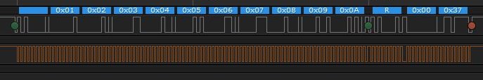
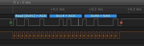
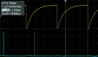
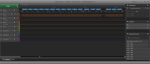
The above two pieces of code are fuller applications and if we execute these and hook up the logic anayser to the I2C bus we see the following output:
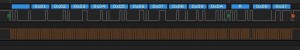
Adding 1 To 10
Reading From Multiple Devices
The I2C protocol allows for one or more devices with different slave addresses to be connected to the same I2C bus. The previous article used the TMP102 temperature sensor with slave address 0x48 and this article has created a slave device with address 0x50. It should therefore be possible to connect the two devices to the same bus and talk to each selectively.
Netduino Application
As with the previous examples, the Netduino 3 will be used as the I2C bus master. The applicaiton above will need to be merged with the code in the previous article.
using Microsoft.SPOT;
using Microsoft.SPOT.Hardware;
using System.Threading;

namespace I2CMaster
{
    public class Program
    {
        public static void Main()
        {
            //
            //  Create a new I2C object and the configurations for the STM8S and the TMP102.
            //
            I2CDevice.Configuration stm8s = new I2CDevice.Configuration(0x50, 50);
            I2CDevice.Configuration tmp102 = new I2CDevice.Configuration(0x48, 50);
            I2CDevice i2cBus = new I2CDevice(stm8s);
            //
            //  Create a transaction to write several bytes of data to the I2C bus.
            //
            byte[] buffer = { 1, 2, 3, 4, 5, 6, 7, 8, 9, 10 };
            byte[] resultBuffer = new byte[2];
            I2CDevice.I2CTransaction[] transactions = new I2CDevice.I2CTransaction[2];
            transactions[0] = I2CDevice.CreateWriteTransaction(buffer);
            transactions[1] = I2CDevice.CreateReadTransaction(resultBuffer);
            //
            //  Create a transaction to read two bytes of data from the TMP102 sensor.
            //
            byte[] temperatureBuffer = new byte[2];
            I2CDevice.I2CTransaction[] reading = new I2CDevice.I2CTransaction[1];
            reading[0] = I2CDevice.CreateReadTransaction(temperatureBuffer);
            while (true)
            {
                //
                //  Read data from the I2C bus.
                //
                i2cBus.Config = stm8s;
                int bytesRead = i2cBus.Execute(transactions, 100);
                i2cBus.Config = tmp102;
                bytesRead = i2cBus.Execute(reading, 100);
                //
                //  Convert the reading into Centigrade and Fahrenheit.
                //
                int sensorReading = ((temperatureBuffer[0] << 8) | temperatureBuffer[1]) >> 4;
                double centigrade = sensorReading * 0.0625;
                double fahrenheit = centigrade * 1.8 + 32;
                //
                //  Display the readings in the debug window and pause before repeating.
                //
                Debug.Print(centigrade.ToString() + " C / " + fahrenheit.ToString() + " F");
                //
                //  Now display the results of the addition.
                //
                string message = "";
                for (int index = 0; index < buffer.Length; index++)
                {
                    message += buffer[index].ToString();
                    if (index == (buffer.Length - 1))
                    {
                        message += " = " + ((resultBuffer[0] * 256) + resultBuffer[1]).ToString();
                    }
                    else
                    {
                        message += " + ";
                    }
                }
                Debug.Print(message);
                Thread.Sleep(1000);
            }
        }
    }
}
The above code creates two I2C configuration object, one for the TMP102 and one for the STM8S device. The I2C bus object has the configuration changed depending upon which device is required.
Wiring up the Devices
Firstly, wire up the TMP102 sensor as described in the article on I2C master devices. The SDA and SCK lines should be connected to 3.3V via 4K7 resistors. Next connect the SDA and SCK lines from the STM8S device to the same point as SDA and SCK lines from the TMP102 sensor. Throw in the logic analyser connections and you get something like this:
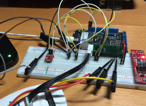
TMP102 and STM8S I2C slave devices
Running the Application
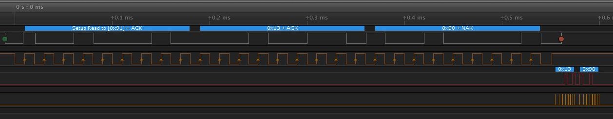
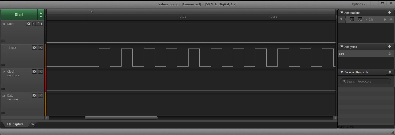
Running the above two applications and starting the logic analyser generated the following output:
Reading From Two I2C Slaves
The write operation to the far left (W0x50) sends the 10 bytes to the STM8S device. This is followed by a read (R0x50) of two bytes from the same device, this can be seen about two thirds of the way from the left-hand side of the trace. The final operation is the read of the current temperature, R0x48, to the right of the trace.
Conclusion
The STM8S slave device above is a simple device. There are still plenty of modification which need to be made:
- Add error handling
- Allow for trapping conditions such as clock stretching
to name but a few. The code above should allow for simple devices to be put together is a short space of time.