RSS

Posts Tagged ‘KiCad’

KiCAD ERC and DRC

Tuesday, April 23rd, 2024

KiCAD ERC DRC Checks Status

2024 saw the release of KiCAD version 8. This release brings a number of new features to both the user interface and the command line interface. One useful feature has been made easier to use, namely the ability to run the Electrical Rules Checks (ERC) and Design Rules Checks (DRC).

What are ERC and DRC?

ERC checks are run on the schematic and the checks verify the schematic against a number of common mistakes. Examples include:

  • Pins not connected to a net (but not marked as not connected)
  • Pin conflicts
  • Missing drivers

DRC runs against the PCB layout and checks the design rules specified in the design. These rules will vary between fabrication houses and include properties such as:

  • Minimum track width
  • Minimum track spacing
  • Hole-to-track spacing limits

Both types of check can be run through the user interface and from the command line. It is the command line interface that we will look at here as this will allow the checks to be run as part of a continuous integration pipeline (in this case a GitHub Action).

KiCAD Docker Container

Initial thoughts about running these checks is to use a docker container. This will allow the use of a script to run the same commands from the desktop as well as through CI. Luckily, the KiCAD project maintain a docker container for just this purpose.

First step, create a script file containing the two commands that we need to run the checks. Our script file will look something like this:

#!/bin/bash

set -e
scriptdir="$( cd "$(dirname "$0")" ; pwd -P )"

kicad-cli sch erc --severity-all --exit-code-violations -o "$scriptdir/erc.rpt" Meadow-Feather-OLED.kicad_sch
kicad-cli pcb drc --severity-all --exit-code-violations -o "$scriptdir/drc.rpt" Meadow-Feather-OLED.kicad_pcb

If we save this file as say run-erc-drc.sh then we can run the checks from the command line using docker to run the script. The command to run the script would look something like this:

docker run --platform linux/amd64 --rm -v $PWD:/project -w /project kicad/kicad:8.0.1 ./run-erc-drc.sh

Note that the –platform option allows the container to run on Apple Silicon Macs as well as Intel platforms. Running the above command will show the following output:

Running ERC...
Checking sheet names...
Checking bus conflicts...
Checking conflicts...
Checking units...
Checking footprints...
Checking pins...
Checking labels...
Checking for unresolved variables...
Checking no connect pins for connections...
Checking for library symbol issues...
Checking for off grid pins and wires...
Checking for undefined netclasses...
Found 0 violations
Saved ERC Report to /project/erc.rpt
Loading board
Running DRC...
Found 0 violations
Found 0 unconnected items
Saved DRC Report to /project/drc.rpt

The run-erc-drc.sh script will generate two report files, one for the ERC and one for the DRC. Checking the erc.rpt file contents will, for a successful run, will show something like this:

ERC report (2024-04-22T18:38:28+0000, Encoding UTF8)

***** Sheet /

 ** ERC messages: 0  Errors 0  Warnings 0

Great, so we now have the docker container created and the report is being generated based upon the current design and PCB layout. The next step is to integrate this into a GitHub Action.

GitHub Action

The first attempt at performing the checks in a GitHub Action resulted in the following yaml file:

name: Run ERC and DRC checks

on:
  repository_dispatch:
  push:
    branches: [ main ]
  pull_request:
    branches: [ main ]

jobs:
  build:
    runs-on: ubuntu-latest

    steps:
    - name: Checkout source code
      uses: actions/checkout@v4

    - name: Run the checks
      run: docker run --platform linux/amd64 --rm -v $PWD:/project -w /project kicad/kicad:8.0.0 ./run-erc-drc.sh
      id: run-the-checks

The theory was to use the same script file in a GitHub Action as was used on the desktop. This will ensure that the checks performed are consistent on both platforms. It would also mean that only one script would need to be maintained.

“Houston We Have a Problem”

Saving a new version of the schematic and pushing the changes to GitHub ran the action and resulted in the following log entries:

11:33:55: Error: can't open file 'erc.rpt' (error 13: Permission denied)
Running ERC...
Checking sheet names...
Checking bus conflicts...
Checking conflicts...
Checking units...
Checking footprints...
Checking pins...
Checking labels...
Checking for unresolved variables...
Checking no connect pins for connections...
Checking for library symbol issues...
Checking for off grid pins and wires...
Checking for undefined netclasses...
Found 0 violations
Unable to save ERC report to erc.rpt
Error: Process completed with exit code 4.

Some time later…

After spending some time with Google and the GitHub help system yielded nothing too helpful regarding solving the issue and removing the error. It was however, discovered that someone had already created a GitHub Action to run the checks anyway. The sparkengineering/kicad-action@v1 action can be used to run the checks. The following yaml file will run the action and perform the ERC and DRC checks:

name: Run ERC and DRC checks

on:
  repository_dispatch:
  push:
    branches: [ main ]
  pull_request:
    branches: [ main ]

jobs:
  RunChecks:
    runs-on: ubuntu-latest

    steps:
    - name: Checkout source code
      uses: actions/checkout@v4

    - name: Run KiCad ERC
      id: erc
      uses: sparkengineering/kicad-action@v1
      if: '!cancelled()'
      with:
        kicad_sch: Meadow-Feather-OLED.kicad_sch
        sch_erc: true

    - name: Run KiCad DRC
      id: drc
      uses: sparkengineering/kicad-action@v1
      if: '!cancelled()'
      with:
        kicad_pcb: Meadow-Feather-OLED.kicad_pcb
        pcb_drc: true

The results of the checks can be shown on the repository home page by creating a badge for the workflow. The badge is then added to the README.md file. The badge will show the status of the checks and will be updated each time the checks are run.

Conclusion

The ready built action does perform the checks required and the badge shows the results of the check workflow. While the method of running the checks are different, both will run the checks giving and indication of success or failure. The desktop script has the advantage of producing a report file that can be reviewed, along with the schematic and PCB layout, to resolve any design issues.

It was disappointing to find that the docker image could not be used within the GitHub Action. There will surely be a simple solution it is just having the time to find it.

An example of the GitHub Action script and a PCB design and layout can be found in the Meadow OLED Feather board repository.

KiCAD Relative Positioning

Sunday, March 10th, 2024

KiCAD Positioning Banner

Most of the PCBs I make have mounting holes in the final layout to allow the boards to be firmly attached to 3D printed cases or mounts. When I first started using KiCAD I found it difficult to position the arc edge cuts around the mounting holes accurately. This was not too critical but it was a little annoying. The error in positioning the arcs was minor and is difficult to see but it would be good to fix the problem.

This was something I finally worked out in the last design I sent to manufacture and thought it would be something others might want to know about.

Board Layout

Most of my designs usually result in a square or rectangular board. The boards are simple and don’t really need to fis an irregularly shaped case. So most of the time I am trying to place a hole at the corner of say a square and then place an edge cut around the hole, something like this:

PCB with two mounting holes

PCB with two mounting holes

Placing the mounting holes is a simple case of editing the x and y positions of the mounting hole and ensuring that the holes are lined up correctly. The edge cuts are a little more difficult to position consistently when placing them by hand.

Accurate Edge Cuts

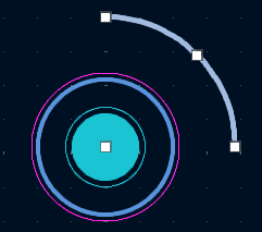
As noted above, the first stage is to place the mounting holes on a rectangular grid and using the x and y positions to place the holes. Next step is to create an arc centred on one of the mounting holes with the appropriate radius. This can be done in using the centre of the mounting holes as the starting point and then sweeping an arc through 90 degrees around the hole:

Arc and Hole

Arc and Hole

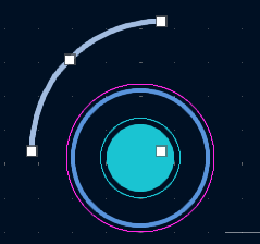
Next up we duplicate the arc, rotate it through 90 degrees and move to one of the opposite mounting holes:

Duplicated arcs

Duplicated arcs

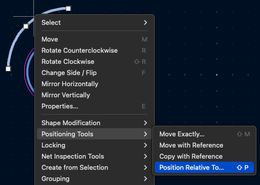
As you can see, the duplicated arc is not centred on the opposite mounting hole. We now use the positioning tools to align the arc with the mounting hole. Start by selecting the arc and then right click to bring up the context menu and select Position Relative To… from the context menu:

Positioning context menu

Positioning context menu

From the positioning dialog click on the Select Item button:

Select item button

Select item button

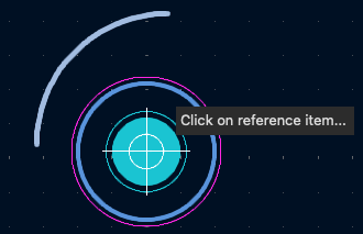
Next, select the reference item, in this case it is the mounting hole:

Select the reference item

Select the reference item

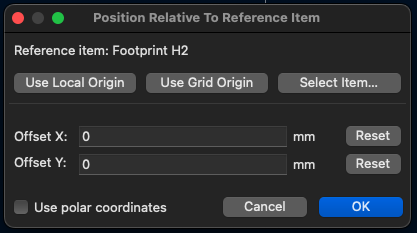
The positioning dialog will now reappear with the reference item selected. Ensure that the Offset X and Offset Y are both set to 0 and click OK.

Position dialog box

Position dialog box

The arc should now move and be centred on the mounting hole.

Final arc position

Final arc position

Finally, repeat for the remaining 2 mounting holes.

Conclusion

This method allows for the board outline to be defined more accurately then lining up the arcs by eye. It is simple to do and only takes a few minutes to complete. The arcs can then be used as the anchors for the linear edges of the board.

This technique is also useful for positioning other parts on any design.

Meadow OLED PCBs

Sunday, January 28th, 2024

Meadow OLED Board Banner Image

A few weeks ago I promised an update on my experience using the PCBWay and Round Tracks plugins for KiCAD.

Well the boards are back and I must say they are looking good.

Rounded Tracks Plugin

The rounded tracks plugin certainly gives the 1970s feel to the PCBs. The batch ordered had a gloss black finish and this made the rounded effect a little difficult to see, a matt finish may have looked better or maybe even a green PCB for that real 1970s vibe.

This plugin has seen a little more use since the first order and here are a few things I have picked up:

  • Apply teardrops after using the plugin
  • Keep the original PCB layout

Adding teardrops to the board really does give the retro feel to the board. I have found that rounding the tracks after adding teardrops can leave a disjoint connection between the track at the teardrop connection to the pad.

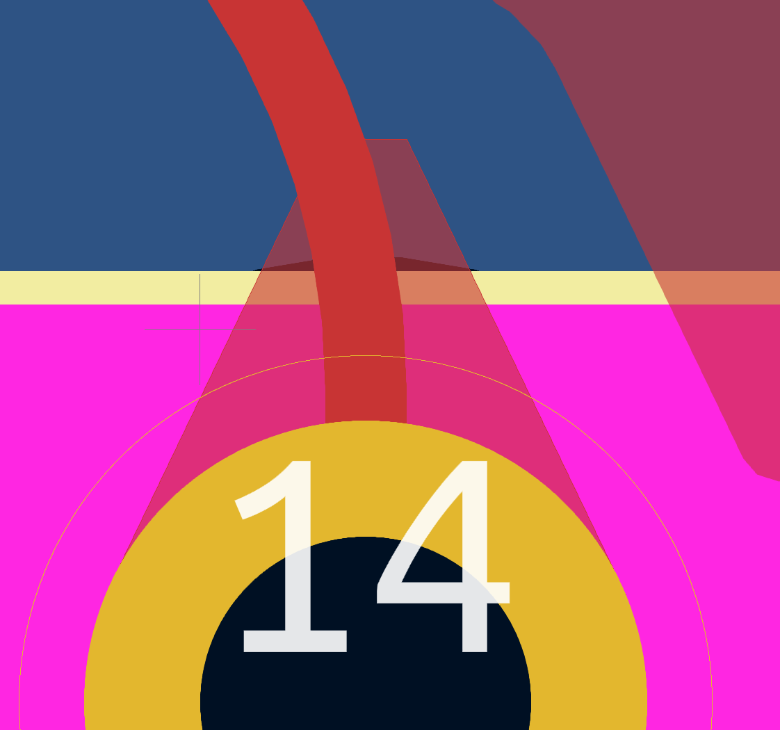
So here is a section of the board with the rounded tracks applied after the teardrops:

Rounded Track Applied After Teardrop

Rounded Track Applied After Teardrop

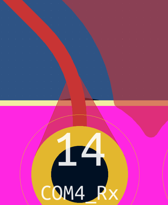
This shows that the track exits the corner of the teardrop which is not ideal. Next we have the same pad with the rounded tracks applied before the teardrops:

Rounded Track Applied Before Teardrop

Rounded Track Applied Before Teardrop

The second case is certainly more aesthetically pleasing.

The plugin asks if you want to apply the changes to the current PCB or if it should create a copy. I went for the halfway house and applied the changes to the PCB, reviewed and ordered the boards and then reverted the changes. This worked well as the plugin ran in under a second and allowed the retention of the original design. It is always going to be easier to apply any changes to the PCB on a board with angular tracks than it is to apply the changes to a board with rounded tracks.

PCBWay Plugin

This plugin really made ordering the PCBs a dream. The only thing to remember is to login to your PCBWay account before attempting to use the plugin. If you do this the plugin will create and upload a ZIP file with the gerbers directly to your PCBWay account. This allows the plugin to set all of the parameters for board dimensions and layers all seamlessly.

Finished Boards

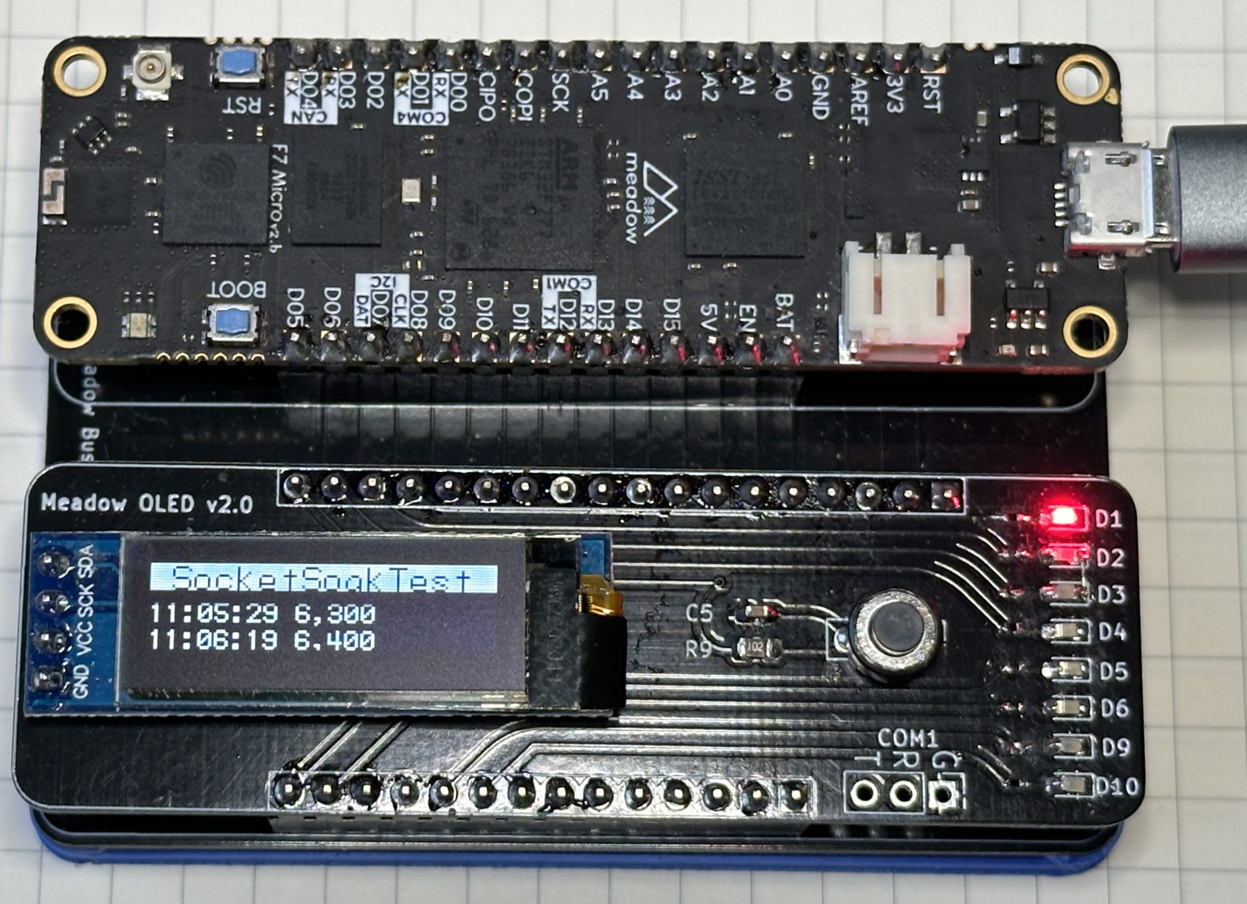
Here is a photo of the finished board connected to a Meadow F7 Micro board running a sok test:

Meadow and OLED Display

Meadow and OLED Display

Conclusion

The Rounded Tracks plugin is only really of interest if you want the retro 1970 look and feel to the final PCB. The PCBWay plugin is really useful as it streamlines the ordering process and removes the need to manually create the gerber files and upload them to the PCBWay website.

Trying Some New KiCad Plugins

Saturday, December 16th, 2023

Meadow PCB Header

A recent change to a PCB design has given the opportunity to try out a couple of KiCad plugins. The board is a simple one and is used to provide feedback when running network soak tests. The board is designed for the Meadow ecosystem and is a fairly simple design consisting of:

  • SSD1306 OLED display
  • Indicator LEDs
  • Reset button
  • Headers to connect the board to a Meadow board

The board has been tested and it works well. The changes doubled the number of LEDs and changed some of the components footprints.

Round Tracks

The concept behind Round Tracks is simple, take a PCB layout and give the tracks the feel of the 1970s. It does this by taking the layout and looking for any tracks that change direction. The plugin then takes these tracks and rounds the corners.

Applying this to the OLED PCBs gives the following output:

Meadow OLED PCB Feather

PCBWay Plug-in for KiCad

The next plugin is the PCBWay plugin. This should take the PCB layout and generate a zip file to upload to the PCBWay web site for manufacture. It appears to be really simple to use and starts an order for you and then uploads the files into the order.

Order submitted and now we just have to wait for the PCBs to arrive.

Conclusion

Manufacturing is complete and they are now on their way. There is going to be a small wait while the PCBs make their way from China to the UK and then we can see how the plugins faired.

Update to follow in a few weeks.