Testing and Simulating Verilog Module for the UPduino FPGA

The previous post installed the toolchain and verified that the tools had been installed. Now it is time to create a project and and run the tools to test and simulate a part. The 74LS245 Bus Transceiver with three state output.
Creating a Project
First step is to create the project directory and create a file containing the PIO project configuration file, apio.ini. Starting a terminal and executing the following commands:
mkdir Project
cd Project
apio create -b upduino31
This should create the apio.ini file in the Project directory containing the board name and the name of the top module. Additional configuration items are defined in the FPGA Wars documentation.
Basic Implementation of the 74LS245
The 74LS245 provides a way of connecting or isolating a circuit to / from a bus. The chip provides a tristate interface. This enables signals to flow in both directions as well as the possibility of isolation from the bus. This device has the following signals / connections:
- 8 Data lines on the A bus connection
- 8 Data lines on the B bus connection
- Direction signal
- Output enable signal
Output Enable (OE) determines if the 74LS245 allows data to flow between the data busses. This is an active low signal so 0 enables the connection and 1 disables the connection.
Direction determines the direction of data, does data flow from bus A to bus B or vice versa? A value ot 0 takes the data signals on bus B and copies them to bus A. 1 connects the busses in reverse.
The basic implementation in Verilog could look something like the following:
//
//  74LS245 - Octal bus transceiver with 3-state outputs.
//
module ttl245_transceiver
#(PROPAGATION_DELAY = 32, RISE_TIME = 1, FALL_TIME = 1)
(
    inout wire [7:0] A,    // 8-bit bidirectional bus A.
    inout wire [7:0] B,    // 8-bit bidirectional bus B.
    input wire DIR,        // Direction control: 0=B to A, 1=A to B.
    input wire OE_n        // Output Enable (active low, tri-state when high).
);
    //
    //  Internal signals for direction control.
    //
    reg [7:0] A_out;
    reg [7:0] B_out;

    //
    // OE  DIR  Function
    // ----------------------
    //  0   0   B to A
    //  0   1   A to B
    //  1   X   Outputs disabled (high-impedance)
    //
    assign A = ((OE_n == 1'b0) && (DIR == 1'b0)) ? A_out : 8'bz;
    assign B = ((OE_n == 1'b0) && (DIR == 1'b1)) ? B_out : 8'bz;

    always @(A or B or DIR or OE_n)
    begin
        if (OE_n == 1'b0) begin
            if (DIR == 1'b1)
            begin
                #PROPAGATION_DELAY B_out <= A;
            end else
            begin
                #PROPAGATION_DELAY A_out <= B;
            end
        end else
        begin
            #(PROPAGATION_DELAY)
            A_out <= 8'bz;
            B_out <= 8'bz;
        end
    end

endmodule
The values for the rise and fall times are not used in this implementation. The propagation delay is used to mimic the fact that signals are not mirrored between the busses immediately.
Testing
APIO offers two methods of checking the implmentation:
- Testing
- Simulation
Both of these methods require a test bench also implemented in Verilog.
//
//  Test the implementation of the 74LS245 octal bus transceiver.
//
`timescale 1 ns / 10 ps

module ttl245_tb();
    reg [7:0] A_drive;
    reg [7:0] B_drive;
    reg DIR;                // Direction control: 1 = A to B, 0 = B to A.
    reg OE_n;               // Output Enable (active low).
    wire [7:0] A;
    wire [7:0] B;

    reg A_enable;
    reg B_enable;

    //
    // Drive A and B buses conditionally.
    //
    assign A = A_enable ? A_drive : 8'bz;
    assign B = B_enable ? B_drive : 8'bz;

    //
    // Instantiate the ttl245_transceiver module using the default propagation delay.
    //
    ttl245_transceiver uut (
        .A(A),
        .B(B),
        .DIR(DIR),
        .OE_n(OE_n)
    );

    localparam PROPAGATION_DELAY = 50;     // Delay to allow for propagation with some overhead.

    initial begin
        $dumpvars(0, ttl245_tb);
    end

    initial begin
        //
        //  Setup the initial conditions.
        //
        A_drive = 8'b00000000;
        B_drive = 8'b00000000;
        DIR = 1'b0;                 // Initial direction B to A.
        OE_n = 1'b1;                // Outputs disabled.
        A_enable = 1'b0;
        B_enable = 1'b0;

        //
        //  Test 1: A to B direction (DIR = 1).
        //
        DIR = 1'b1;              // Set direction A to B.
        OE_n = 1'b0;             // Enable output.
        A_enable = 1'b1;         // Drive A bus.
        B_enable = 1'b0;         // Release B bus (will be driven by chip).
        A_drive = 8'b10101010;   // Drive A with test pattern.
        #PROPAGATION_DELAY
        if (B != A_drive) begin
            $error("Error: Test 1a, B bus did not match expected value.");
        end

        //
        //  More tests go here.
        //

        $display("74LS254 - End of Simulation");
        $finish;
    end

endmodule
The code above shows just one test with the insertion point for further tests to be added. The two files (implmentation and test bench) should be placed in the Project directory and the following structure is suggested:
Project/
├── apio.ini
├── Source/
│ └── ttl245.v
├── Tests/
│ └── ttl245_tb.v
APIO will process all of the files in the current directory and any subdirectories. It also expects that the files with the suffix _tb are test bench files.
Running the Test
The tests can be run using the apio test. This command takes an optional file name which when specified will run the tests in the specified file. So the command:
apio test Tests/ttl245_tb.v
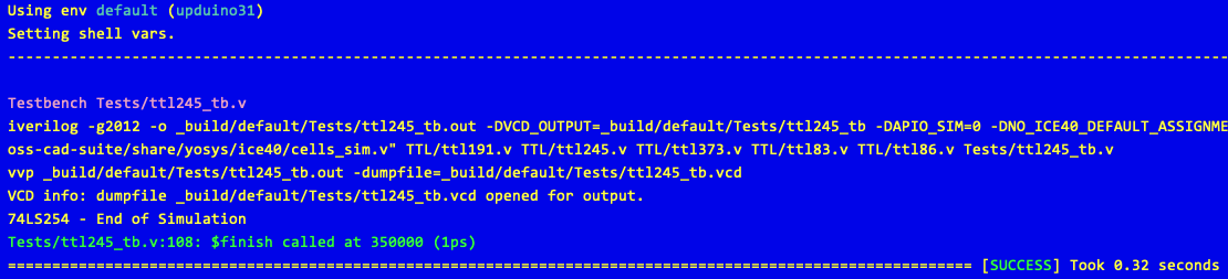
will run the tests in the file Tests/ttl245_tb.v. Running this command results in output similar to the following:
APIO can also run all of the test benches (files with the _tb suffix) with the command:
apio test
In this case this will run the only test bench file. It will run the tests in all of the _tb files if more that one exists.
Simulation
Another option is to run a test bench in simulation mode. In this mode the run output is displayed in gtkwave. This output is useful for displaying the relationship between various signals. A simulation is run using the following command:
apio sim Tests/ttl245_tb.v
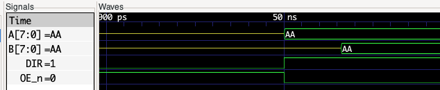
This will run the simulation and collect the output in a vcd file. This is then processed and gtkwave started. Zooming in on the output we can see the data being loaded on to the busses and the signals showing the relationship between the A, B, DIR and OE_n signals:
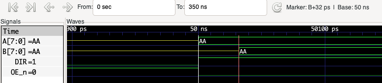
By placing markers we can measure the propagation delay between the data appearing on the A bus and the same data being transferred to the B bus:
By default, APIO starts gtkwave and waits until gtkwave exits before returning control to the terminal. It is possible to return control to the terminal immediately using the command:
apio sim Tests/ttl245_tb.v --detach
Conclusion
It is looking promising so far, it should be possible to build the individual chips in the design and finally combine instances of the chips into a fuller design.
Next up, identify the 7400 chips required and implement the chips and test benches.
Tags: Electronics, FPGA
Thursday, January 1st, 2026 at 12:01 am • Electronics, FPGA • RSS 2.0 feed • leave a response or trackback
