Simulating A 74HC373 Latch
Some of my current projects are starting to require the use of 7400 series logic chips. Prototyping circuits with these chips gives me two obvious options:
- Breadboarding
- FPGA, simulation and implementation
Both of these will allow a prototype to be build but the only way to ensure the FPGA circuit works will be to implement the circuit on breadboard. The simulation option does offer two advantages over breadboarding, namely the ability to simulate and most importantly the chance to work out how to use FPGAs and the associated software.
Given the choice there is really only one option as I need to gain experience of VHDL, bring on the FPGA.
74*373 – Octal Transparent Latch with Three State Output
This is an interesting choice for simulation as the Xilinx software issues a warning about the creation of a latch when clocks are not used for synchronisation of signals. The reason for choosing this chip is simply the fact that this is one of the first chips I will be using in a larger project.
First Implementation
This first implementation concentrated on the functional definition of the latch. Examination of the data sheet for the chip describes the function as follows:
| OE (active low) | LE (active low) | Data | Output |
| L | H | H | H |
| L | H | L | L |
| L | L | l | L |
| L | L | h | H |
| H | X | X | Z |
Where L = Low, H = High, Z = High impedance, X = Don’t care, l = low (h = high) as the signal appeared one setup period ago.
A quick implementation of this could be something like the following:
library ieee;
use ieee.std_logic_1164.all;

--
--  Define the interface for this module.
--
entity HC74373 is
    port
    (
        signal le : in  std_logic;
        signal oe : in  std_logic;
        signal dataIn : in  std_logic_vector (7 downto 0);
        signal dataOut : out  std_logic_vector (7 downto 0)
    );
end HC74373;

--
--  Behaviour of the model.
--
architecture Behavioral of HC74373 is
    --
    --  Store the data in the latch for output.
    --
    signal data : std_logic_vector (7 downto 0) := "00000000";
    --
    --  Temporary store for this model.  This will eventually be
    --  the output.
    --
    signal output : std_logic_vector (7 downto 0) := "ZZZZZZZZ";
begin
    process (le, oe, dataIn, data) is
    begin
        --
        --  When LE is low, the data on the input is stored in the latch.
        --
        if (le = '0') then
            data <= dataIn;
        end if;
        --
        --  When OE is low, the data in the latch is output,
        --  otherwise the output is high impedance.
        --
        if (oe = '0') then
            if (le = '1') then
                output <= dataIn;
              else
                output <= data;
            end if;
          else
            output <= "ZZZZZZZZ";
        end if;
    end process;
    --
    --  Set the output to either the data in the latch or high impedance.
    --
    dataOut <= output;
end Behavioral;
A test bench is needed to simulate the behaviour of the latch.
library ieee;
use ieee.std_logic_1164.ALL;

-- Uncomment the following library declaration if using
-- arithmetic functions with Signed or Unsigned values
--USE ieee.numeric_std.ALL;

entity HC74373TestBench is
end HC74373TestBench;

architecture behavior OF HC74373TestBench is
    component HC74373
    port
    (
         le : in  std_logic;
         oe : in  std_logic;
         dataIn : in  std_logic_vector(7 downto 0);
         dataOut : out  std_logic_vector(7 downto 0)
    );
    end component;

   --Inputs
   signal le : std_logic := '1';
   signal oe : std_logic := '1';
   signal dataIn : std_logic_vector(7 downto 0) := (others => '0');

 	--Outputs
   signal dataOut : std_logic_vector(7 downto 0);
begin

	-- Instantiate the Unit Under Test (UUT)
    uut: HC74373 PORT MAP
    (
        le => le,
        oe => oe,
        dataIn => dataIn,
        dataOut => dataOut
    );

    process
    begin
        --
        --  Initial condition, latch should have stabilised and be high impedance.
        --
        wait for 100 ns;
        --
        --  Set data in to all zeroes, output should still be high impedance.
        --
        le <= '0';
        wait for 20 ns;
        --
        --  Now enable the output.
        --
        oe <= '0';
        wait for 20 ns;
        --
        --  Now set the data in whilst latch and output enable are both allowed.
        --  Data output should become 11110000.
        --
        dataIn <= "11110000";
        wait for 20 ns;
        --
        --  Turn off the latch enable and set the data in bits.  The data output
        --  should not change.
        --
        le <= '1';
        dataIn <= "11001100";
        wait for 20 ns;
        --
        --  Re-enable the output, should become 11110000 as 11001100 has not
        --  been latched yet.
        --
        oe <= '1';
        wait for 20 ns;
        --
        --  Output is turned off, latch the data and enable the output.
        --
        le <= '0';
        wait for 20 ns;
        le <= '1';
        oe <= '0';
        wait for 20 ns;
        --
        --  End of test.
        --
        wait;
    end process;
end;
If we use the above test bench to simulate this then we get the following output:
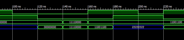
74HC373 Simulated Output
The simulation above shows the circuit running at an equivalent 50 MHz (test bench delays of 20ns). I will be working at a lot slower speed. I anticipate the maximum clock speed to be around 8 MHz (125ns clock) and so the delays in the test bench will be adjusted accordingly.
Propagation Delay
From the simulation we can see that we have emulated the function of the latch with one minor exception, namely timing. In the above zoomed in trace we can see that the input of the latch is immediately reflected on the output pins. In reality this is not what happens as the circuit takes a small amount of time to respond to the input changes. This time is the propagation delay of the chip.
The propagation delay depends upon the change being made and the operating conditions of the circuit. The data sheets often quote several values for the delay. These will vary depending upon factors such as supply voltage and temperature. For the purpose of this post we will assume that the circuit is operating with a supply voltage of 4.5V and at room temperature. The values for the delays are also quoted as minimum, typical and maximum values.
The delays for the 74HC373 are:
| Value | Delay (ns) |
| Data to Output | 30 |
| LE to Output | 35 |
| OE to Data | 30 |
| tsetup | 12 |
If we are going to add these to the model then it may be better to consider breaking up the process into two or more processes each dealing with only a few signals.
The first process deals with latching the data:
process (le, dataIn) is
begin
    --
    --  When LE is low, the data on the input is stored in the latch.
    --
    if (falling_edge(le) or (le = '0')) then
        data <= dataIn after 12 ns;
    end if;
end process;
The above code will store the data in the internal buffer (the latch) if the latch enable pin changes or the data changes and the latch enable pin is low. The data is stored 12ns after the change (as defined in the data sheet).
The second process deals with the output from the latch:
process (oe, dataIn, data) is begin — — When OE is low, the data in the latch is output, — otherwise the output is high impedance. — if (oe = ‘0’) then if (le = ‘1’) then output <= dataIn after 30 ns; else output <= data after 30 ns; end if; else output <= "ZZZZZZZZ" after 30 ns; end if; end process;
This code uses a default 30ns propagation delay for all signals. This is not exactly right but should be good enough for our purposes.
Running the simulation generates the following output (Remember, the delays in the test bench have been adjusted to 125ns):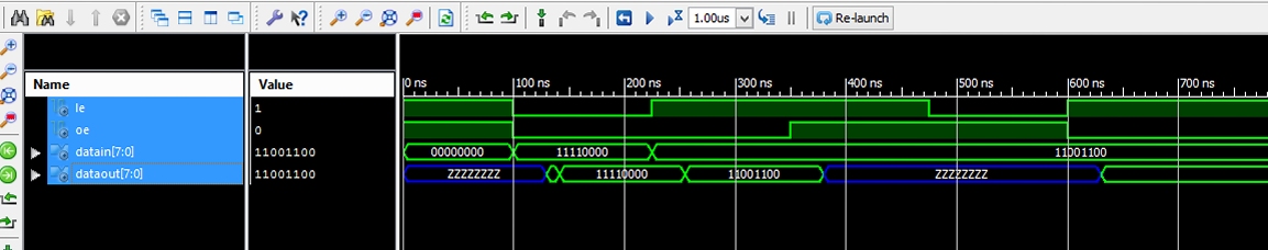
74HC373 Simulated Output With Propagation Delays
We should perhaps look at the delay times in the above process as when that data is latched and also then output through dataOut the code will actually delay the output of the data for 42ns (12 from the latch process and 30 from the output process) when we are actually aiming for a 30ns delay. An exercise for another time.
Conclusion
I now have a latch which will operate at speeds of 8 MHz and I can now start to use this as a component in larger circuits. All that is needed now is a few more components and I can start to simulate larger circuits.
Along the way I have also found a few component libraries at least one of which contained a simulation of this component. Creating this component rather than use a standard library has allowed me to explore and understand more about the Xilinx software. Next step is to look at these libraries and compare this component.
Tags: Electronics, FPGA
Wednesday, December 25th, 2013 at 10:31 am • Electronics, FPGA • RSS 2.0 feed Both comments and pings are currently closed.