When starting with a new development board I always revisit the fundamentals like GPIO. Doing this helps establish that the development tools are working and gives a basic library for future development. So with this post we will be looking at GPIO on the STM32 Discovery board. When Rediscovering the STM32 Discovery Board I mentioned that I would need to look at using either the standard peripheral library provided by ST or to use a lower level method of controlling the board. After due consideration I have decided to continue with the lower level access. Whilst this may be more effort it does lead to a better understanding of what is actually happening at the low level.
Our objective today will be to toggle a GPIO pin (Port D, pin 0) generating a square wave. The result will be something similar to the Simple GPIO post for the STM8S.
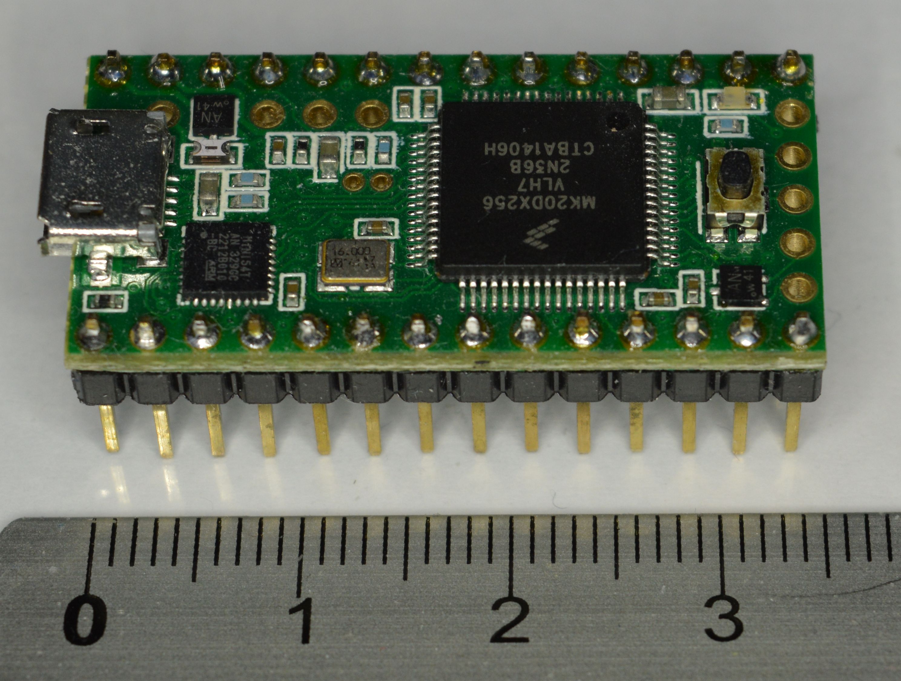
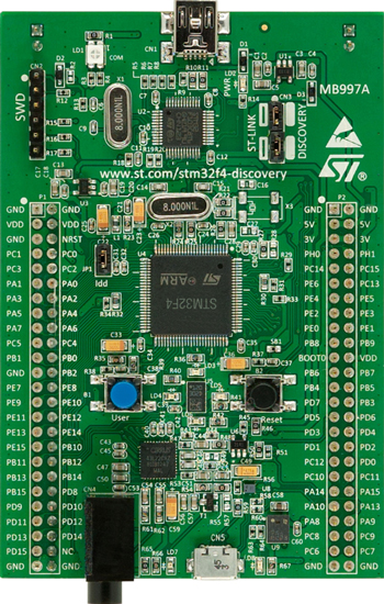
STM32F4 Discovery Board
The STM32F4 Discovery board is a low cost development board for hobbyists, beginners and experienced users. The board uses the STM32F407VGT6 and hosts a number of sensors including digital accelerometer, push buttons, microphone and DAC. It also contains four built in LEDs which can be used to give feedback to the developer and breakout pins for the GPIO ports.
STM32F4 Discovery Board
Each of the GPIO pins can be used for simple input/output of digital signals. The majority of the pins are also mapped to one or more alternative functions. For instance, Port C, pin 3 is also mapped to the following alternative functions:
- SPI2 MOSI
- I2S2 SD
- OTG HS ULPI NXT
- ETH MI TX Clk
- EVENTOUT
For the remainder of this post we will restrict ourselves to the GPIO functionality of the chip and demonstrate the following:
- Output a digital signal on a single GPIO pin
- Flash one of the LEDs on the board
The alternative functionality will be considered in future posts.
The functionality of the 16 pins on each of the GPIO ports is controlled by a number of registers. The description of each of the registers can be found in RM0090 Reference Manual for the STM32 chip. This manual can be downloaded from STs web site.
GPIO Registers
Each STM32 chip has a number of ports each of which has 16 pins. As already noted, each of these pins has a number of functions, the most basic of which is digital input/output. The functionality and state of each port is controlled by a number of GPIO registers:
- Four configuration registers
- Two data registers
- One set/reset register
- One locking register
- Two alternative function registers
An overview of the registers follows; a fuller description of the registers can be found in section 7 of RM0090 Reference Manual (Revision 4).
When referring to the registers, the reference manual uses the following notation:
GPIOx_Function
Where x is replaced by the port to be used. For instance, GPIOx_MODER refers to the generic mode register for a GPIO port. A specific instance of this would be GPIOD_MODER. This refers to the mode register for port D. Normally, x is in the range A to I and is defined by the specific version of the STM32 being used in the project.
Configuration Registers
The STM32 has four configuration registers for each of the ports.
- Port mode register – GPIOx_MODER
- Output type register – GPIOx_OTYPER
- Speed register – GPIOx_OSPEEDR
- Pull-up/Pull-down register – GPIOx_PUPDR
Each of these registers is 32-bits wide although not all of the bits are used in all of the registers.
This 32 bit register holds 2 bit values which defines the operation mode. The modes allowed are:
| Bit Values | Description |
| 00 | Input |
| 01 | General purpose output |
| 10 | Alternate function |
| 11 | Analog |
In general, the default reset value for this register is 0. Some of the ports are reset to non-zero values as the pins in the port have special meanings (debugging pins etc). The rest values are:
| Port | Reset Value |
| A | 0xA800 0000 |
| B | 0x0000 0280 |
| All others | 0x0000 0000 |
The bits in the register are read/write and are in consecutive pairs. So bits 0 & 1 define the mode for pin 0, bits 2 & 3 define the mode for pin 1 etc.
Output Type Register – GPIOx_OTYPER
This is a 32-bit register but only the lower 16 bits are used. The top 16 bits are reserved and should not be used. This register uses a single bit for each pin to define the output type of the pins in the port. So, bit 0 defines the output type for pin 0, bit 1 for pin 1 etc.
| Bit Value | Description |
| 0 | Push/pull output |
| 1 | Open drain output |
The default reset value for all of the GPIOx_TYPER registers is
0x0000 0000 meaning that all ports are configured for push/pull output.
Speed Register – GPIOx_OSPEEDR
This 32-bit register uses all of the bits in the register in pairs (similar to the port mode register). The bits define the output speed of the port. The bit pairs have the following meaning:
| Bit Values | Description |
| 00 | 2 MHz Low speed |
| 01 | 25 MHz Medium speed |
| 10 | 50 MHz Fast speed |
| 11 | 100 MHz High speed on 30pF
80 MHz High speed on 15 pF |
The reset value for these registers is 0x0000 00C0 for port B and 0x0000 0000 for all other registers.
Pull-up/Pull-down register – GPIOx_PUPDR
This 32-bit register uses all of the bits in the register in pairs (similar to the port mode register). The bits define pull-up / pull-down resistor mode for the pins on a port. The bit pairs have the following meaning:
| Bit Values | Description |
| 00 | No pull-up or pull-down resistor |
| 01 | Pull-up resistor |
| 10 | Pull-down resistor |
| 11 | Reserved |
The reset values for the registers are:
| Port | Reset Value |
| A | 0x6400 0000 |
| B | 0x0000 0100 |
| All others | 0x0000 0000 |
Data Registers
The two data registers for each port indicate the input/output state of the port. Each of the registers are 32-bit registers but only the lower 16 bits are used. The top 16 bits are reserved and should not be used.
- Input data register – GPIOx_IDR
- Output data register – GPIOx_ODR
Input data register – GPIOx_IDR
The input data register indicates if a high or low signal has been applied to the pin within a port. The register is read-only and the whole word should be read.
| Bit Value | Description |
| 0 | High logic value |
| 1 | Low logic value |
As with the output type register – GPIOx_OTYPER, the bits in the register map onto the pins in the port (bit 0 maps to pin 0, bit 1 to pin 1 etc.).
The reset value for all of these registers is 0x0000 XXXX where X indicates that the bits are unknown as they will be defined by the input signals applied to the pins are reset.
The output data register allows the program to change the output state of a pin within the port. This is a 32-bit register and only the lower 16 bits are used. The top 16 bits are reserved and should not be used. The output states are defined as:
| Bit Value | Description |
| 0 | High logic value |
| 1 | Low logic value |
As with the output type register – GPIOx_OTYPER, the bits in the register map onto the pins in the port (bit 0 maps to pin 0, bit 1 to pin 1 etc.). The bits in the lower 16 bits of the register are all read/write bits.
The reset value for all of these registers is 0x0000 0000.
A more effective way of setting/resetting a bit in the output register is to use the bit set/reset register.
Set/reset register
The set/reset register sets or resets a single bit in the output data register.
Bit Set/Reset Register – GPIOx_BSSR
This is a 32-bit register and it is split into two halves, the lower 16 bits are used for setting a bit and the upper 16 bits are used for resetting a bit. This is a write only register; reading this register will return 0x0000.
Setting a bit in the lower 16-bits of this register will cause the corresponding bit in the output data register to be set to 1.
Similarly, setting a bit in the upper 16-bits of this register will cause the corresponding bit in the output data register to be set to 0.
For the lower 16-bits the mapping is simple, bit 0 in GPIOx_BSRR maps to bit 0 in GPIOx_ODR etc. For the upper 16-bits, bit 16 of the GPIOx_BSRR maps to bit 0 of the GPIOx_ODR; bit 17 of GPIOx_BSRR maps to bit 1 of GPIOx_ODR etc.
So why provide the set/reset functionality when you have the output data registers? The set/reset register provide an atomic method of setting or resetting an output pin on a port. When using the output data registers, the compiler will have to generate a number of statements in order to set or reset a pin. This can allow an interrupt to be processed when part way through the set/reset operation. By using this register it is possible to set or reset a pin using a single instruction. This means that the operation will complete before the interrupt can be processed.
Configuration Lock Register
This register is used to lock the configuration of the port until the next reset of the chip.
Configuration Lock Register – GPIOx_LCKR
The register is a 32-bit register but only 17 bits are actually used. The lower 16 bits indicate which bit of the port configuration is locked. So setting bit 0 of the register will lock the configuration of pin 0 etc.
The final bit used is bit 16 in the register (known as the Lock Key – LCKK); this bit determines the lock status of the port; a zero indicates that no lock is applied whilst a 1 indicates that the port configuration is locked.
In order to lock the configuration of a port the configuration lock write sequence must be followed. This will prevent accidental locking of the port configuration. The algorithm for locking the configuration is as follows:
- Set bits 0 through 15 of the register indicating which pins should have their configuration locked
- Set LCKK to 1 and write the value into the register
- Set LCKK to 0 and write the value into the register
- Set LCKK to 1 and write the value into the register
- Read the lock bit of the port
It is important to note that the values in bits 0 through 15 should not change whilst following the above sequence. Should they change or any error occur then the lock will be aborted.
The final step, reading the lock bit, confirms the success or failure of the operation.
Alternative function registers
The alternative function registers allow the configuration of the port to change from simple GPIO to an alternative function such as SPI MOSI. These registers are noted here but will not be discussed further as they will be covered in subsequent posts.
C Definitions and Some Typedefs
The register in the STM32 microcontroller have been mapped onto specific memory locations within the valid address space of the STM32. These memory locations are defined in the various header files for the microcontroller. For instance, the following type definition has been taken from the header file stm32f4xx.h:
typedef struct
{
  __IO uint32_t MODER;    /*!> GPIO port mode register,               Address offset: 0x00      */
  __IO uint32_t OTYPER;   /*!> GPIO port output type register,        Address offset: 0x04      */
  __IO uint32_t OSPEEDR;  /*!> GPIO port output speed register,       Address offset: 0x08      */
  __IO uint32_t PUPDR;    /*!> GPIO port pull-up/pull-down register,  Address offset: 0x0C      */
  __IO uint32_t IDR;      /*!> GPIO port input data register,         Address offset: 0x10      */
  __IO uint32_t ODR;      /*!> GPIO port output data register,        Address offset: 0x14      */
  __IO uint16_t BSRRL;    /*!> GPIO port bit set/reset low register,  Address offset: 0x18      */
  __IO uint16_t BSRRH;    /*!> GPIO port bit set/reset high register, Address offset: 0x1A      */
  __IO uint32_t LCKR;     /*!> GPIO port configuration lock register, Address offset: 0x1C      */
  __IO uint32_t AFR[2];   /*!> GPIO alternate function registers,     Address offset: 0x20-0x24 */
} GPIO_TypeDef;
This header file can be found in the Standard Peripheral Library as supplied by ST Microelectronics.
A careful examination of the members of the struct within the typedef reveals that with one exception, the members of the struct all map directly onto the registers we have been discussing above. The one exception is the BSSR register. This has been split into two components BSSRL and BSSRH. This split nicely maps to the difference in functionality of the two halves of the register, namely Setting and resetting of individual bits in the output data register.
Locating A GPIO in Memory
Once we have the layout of the registers (as defined in the struct above), we simply need to map the structure onto the right location in memory. A little further digging in the header file leads us to the following #define statements:
#define GPIOD             ((GPIO_TypeDef *) GPIOD_BASE)

#define GPIOD_BASE        AHB1PERIPH_BASE + 0x0C00)

#define APB1PERIPH_BASE   PERIPH_BASE

#define PERIPH_BASE       ((uint32_t) 0x40000000) /*!< Peripheral base address in the alias region                                */
Following the chain of #define statements leads us to the the conclusion that the registers for GPIOD are located at memory location 0x40000C000. These definitions mean that we should be able to access individual registers with statements such as:
GPIOD->MODER = 0x01; // Set Pin 0 of Port D to input.
A Practical Demonstration
After all this theory we must be ready for some coding. In this section we will look at creating two small applications:
- GPIO Toggle – toggling a single pin on a GPIO port
- Blinky – Flashing a single LED
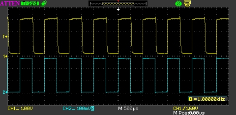
The first of the two applications will simply toggle a single GPIO pin as fast as possible using the default reset state of the microcontroller. Note that an oscilloscope will be required in order to prove that the application is working correctly
The second application will make use of the on board LEDs. This will require a little more coding in order to provide a delay between turning the LED on and off in order to make the flashing visible to the naked eye.
Application 1 – Toggling A GPIO Pin
This application is simple and consists of two parts:
- Initialisation
- A loop which toggles the GPIO pin
The full application looks like this:
#include "stm32f4xx_rcc.h"
#include "stm32f4xx_gpio.h"

int main()
{
    //
    //  Initialise the peripheral clock.
    //
    RCC->AHB1ENR |= RCC_AHB1Periph_GPIOD;
    //
    //  Initilaise the GPIO port.
    //
    GPIOD->MODER |= GPIO_Mode_OUT;
    GPIOD->OSPEEDR |= GPIO_Speed_25MHz;
    GPIOD->OTYPER |= GPIO_OType_PP;
    GPIOD->PUPDR |= GPIO_PuPd_NOPULL;
    //
    //  Toggle Port D, pin 0 indefinitely.
    //
    while (1)
    {
        GPIOD->BSRRL = GPIO_Pin_0;
        GPIOD->BSRRH = GPIO_Pin_0;
    }
}
One thing to note from the above code is that we need to initialise the peripheral clocks (this should be taken as read for the moment and will be covered in future posts). When initialising the GPIO port we should take into consideration the default clock speed of the Discovery board after reset. By default this is 8 MHz and so we should set the speed of the output port accordingly. This leads to a configuration for pin 0 of output with a maximum speed of 25 MHz, push pull with not pull-up or pull-down resistors.
Once initialised we enter the main program loop. Here the application uses the set/rest registers to toggle pin 0. This shows how the 32-bit register is split into two, one for the set and one for the reset operation.
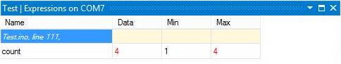
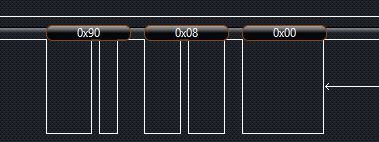
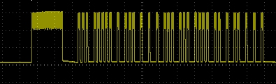
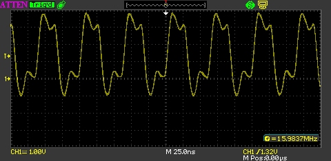
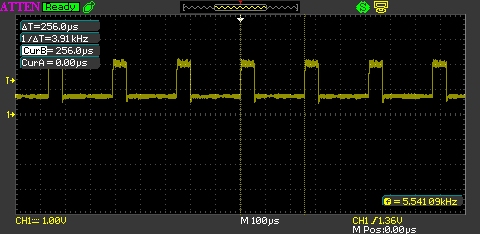
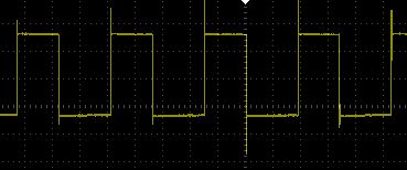
If we create a simple STM32 project using IAR, compile and then deploy this application we get the following output on the oscilloscope:
STM32 Scope Output
And there we have it, our first application deployed to the STM32 Discovery board.
Blinky – Flashing A Single LED
This second example is really aimed at those who do not have access to an oscilloscope. Here we will slow down the output of the GPIO port and flash one of the built in LEDs.
The STM32F4 Discovery board has four built in LEDs which can be accessed by setting/resetting pin 12 through 15 on port D. The LED colours are:
| Pin Number | Colour |
| 12 | Green |
| 13 | Orange |
| 14 | Red |
| 5 | Blue |
Using the code in the previous example as a starting point we find ourselves with an application which looks something like this:
#include "stm32f4xx.h"
#include "stm32f4xx_gpio.h"
#include "stm32f4xx_rcc.h"

#define LED_GREEN      12
#define LED_ORANGE     13
#define LED_RED        14
#define LED_BLUE       15

int main()
{
    int pin = LED_RED;
    uint32_t mode = GPIO_Mode_OUT << (pin * 2);
    uint32_t speed = GPIO_Speed_100MHz << (pin * 2);
    uint32_t type = GPIO_OType_PP << pin;
    uint32_t pullup = GPIO_PuPd_NOPULL << (pin * 2);
    //
    //  Initialise the peripheral clock.
    //
    RCC->AHB1ENR |= RCC_AHB1Periph_GPIOD;
    //
    //  Initilaise the GPIO port.
    //
    GPIOD->MODER |= mode;
    GPIOD->OSPEEDR |= speed;
    GPIOD->OTYPER |= type;
    GPIOD->PUPDR |= pullup;
    //
    //  Toggle the selected LED indefinitely.
    //
    int index;
    while (1)
    {
        GPIOD->BSRRL = (1 << pin);
        for (index = 0; index < 500000; index++);
        GPIOD->BSRRH = (1 << pin);
        for (index = 0; index < 500000; index++);
    }
}
Deploying this application should flash the selected LED just below the STM32 microcontroller on the STM32F4 Discovery board.
Conclusion
This post presented two simple applications which toggle GPIO lines on Port D. Using these techniques and the additional information in the register descriptions you should be able to extend the application above to control digital devices such as shift registers etc.