RSS

Archive for the ‘Software Development’ Category

UDP on the ESP01 (ESP8266 Development Board)

Monday, June 1st, 2015

ESP8266 boards offer an amazing opportunity to explore the IoT world at a low cost. The boards start for as little as £5 here in the UK and come in a variety of form factors from one with only two GPIO pins to larger boards containing more GPIOs, PWM, I2C, SPI and analog capability. The boards started to become noticed around the middle of 2014 and have become more popular as the tools and documentation have matured.

Support for the boards is mainly through the online community forum. The latest documentation and SDKs can be found through the same forums.

The boards make low cost networks of sensors a possibility with the ESP8266 modules acting as either small servers or clients on your WiFi network.

The ESP8266 module is often supplied with one of two firmware version burned into the module:

  1. nodeMCU – Lua interpreter
  2. AT command interpreter

For the purposes of this exercise we will look at replacing the default firmware supplied with a custom application.

The SDK available from Expressif allows the developer to program the module using C. First thing to do is to install the tool chain for the module. The ESP8266 Wiki contains a host of information including instructions on setting up the tools on a variety of platforms. This whole process took about 2-3 hours on my Windows PC with another few hours to put together a template for a makefile application for Visual Studio.

Now that the development tools are in place we can start to think about the sensor network. Security is a major concern for Internet of Things (IoT) projects but this proof of concept will ignore this for the moment and rely on the WiFi encryption as the only mean of securing the data. This is a proof of concept afterall.

The applications developed here will allow data to be transmitted using UDL over the local area network.

UDP Receiver

Before starting on the ESP8266 application we should put together a simple application to receive the data from the local network. A simple .NET application on a Windows PC should do the trick:

using System;
using System.Collections.Generic;
using System.Text;
using System.Threading.Tasks;
using System.Net;
using System.Net.Sockets;

namespace UDPConsoleClient
{
    class Program
    {
        static UdpClient _udpClient = new UdpClient(11000);

        static void Main(string[] args)
        {
            Console.WriteLine("UDP Client listening on port 11000");
            IPEndPoint _remoteEndPoint = new IPEndPoint(IPAddress.Any, 0); 
            while (true)
            {
                byte[] data = _udpClient.Receive(ref _remoteEndPoint);
                string message = Encoding.ASCII.GetString(data);
                Console.WriteLine("Message ({0}): {1}", _remoteEndPoint.Address.ToString(), message);
            }
        }
    }
}

Create a new Windows console application on the PC and add the above code to the program.cs file. When run, this application will listen to the local network and display any UDP packets as a string to the console. Nothing special but good enough for the purposes of this experiment.

Basic ESP8266 Application

The basic ESP8266 application works in a similar way to an Arduino application, there is an initialisation method user_init and a loop method. The loop method is slightly different from the Arduino loop in that it is added to a task queue and the developer is free to select the name of the method. A basic application looks something like this:

#include "at_custom.h"
#include "ets_sys.h"
#include "osapi.h"
#include "gpio.h"
#include "os_type.h"
#include "mem.h"
#include "user_config.h"
#include "ip_addr.h"
#include "espconn.h"
#include "user_interface.h"

#define USER_TASK_PRIORITY          0
#define USER_TASK_QUEUE_LENGTH      1

//
//  Callbacks for the OS task queue.
//
os_event_t userTaskQueue[USER_TASK_QUEUE_LENGTH];

//
//  User function which will be added to the task queue.
//
static void ICACHE_FLASH_ATTR UserTask(os_event_t *events)
{
    os_delay_us(10);
}

//
//  Initialise the application and add the user task to the task queue.
//
void ICACHE_FLASH_ATTR user_init()
{
    //
    //  Start OS tasks.
    //
    system_os_task(UserTask, USER_TASK_PRIORITY, userTaskQueue, USER_TASK_QUEUE_LENGTH);
}

Compiling and deploying this application will result in a module which does nothing much other than wait.

Debugging

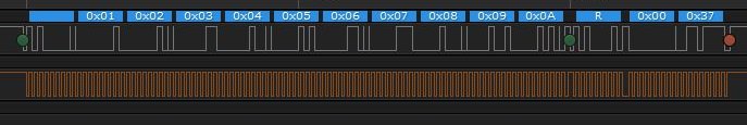
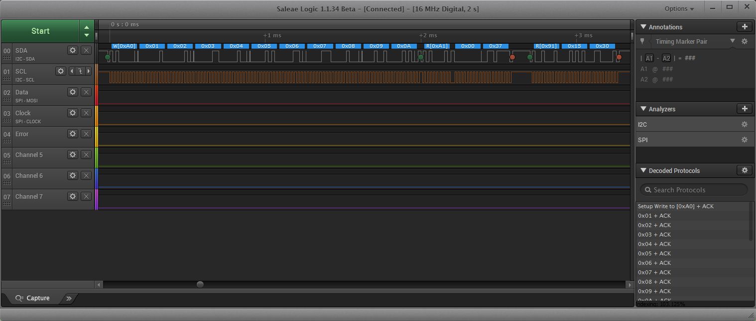
Unlike some of the other modules and boards discussed on this blog, the ESP8266 does not have much available in the way of debugging. Code will need to be added to the application to output debug information on GPIO pins in order to get feedback on what is going on inside the application.

The ESP01 module being used has two GPIO pins available, GPIO0 and GPIO2. We can use these to output serial data akin to SPI and then use a logic analyser to examine the application state. Adding the code below will allow us to do this.

#define BB_DATA                     BIT0
#define BB_CLOCK                    BIT2

//
//  Initialise the GPIO pins.
//
void InitialiseGPIO()
{
    gpio_init();
    //
    //  Set GPIO2 and GPIO0 to output mode.
    //
    PIN_FUNC_SELECT(PERIPHS_IO_MUX_GPIO2_U, FUNC_GPIO2);
    PIN_FUNC_SELECT(PERIPHS_IO_MUX_GPIO0_U, FUNC_GPIO0);
}

//
//  Bit bang the data out as serial (SPI) data.
//
void BitBang(uint8 byte)
{
    //
    //  Set the clock and data bits to be low.
    //
    gpio_output_set(0, BB_DATA, BB_DATA, 0);
    gpio_output_set(0, BB_CLOCK, BB_CLOCK, 0);
    //
    //  Output the data.
    //
    short bit;
    for (bit = 7; bit >= 0; bit--)
    {
        if (byte & (1 << bit))
        {
            gpio_output_set(BB_DATA, 0, BB_DATA, 0);
        }
        else
        {
            gpio_output_set(0, BB_DATA, BB_DATA, 0);
        }
        gpio_output_set(BB_CLOCK, 0, BB_CLOCK, 0);
        gpio_output_set(0, BB_CLOCK, BB_CLOCK, 0);
    }
    //
    //  Set the clock and data bits to be low.
    //
    gpio_output_set(0, BB_DATA, BB_DATA, 0);
    gpio_output_set(0, BB_CLOCK, BB_CLOCK, 0);
}

Timers

For the proof of concept the application can simply generate a regular packet of data emulating the presence of sensor data. The most cost effective (in terms of power) way of doing this will be to use a timer of some sort.

//
//  OS Timer structure holding information about the timer.
//
static volatile os_timer_t timerInformation;

//
//  Timer function called periodically - try communicating with the world.
//
void TimerCallback(void *arg)
{
    BitBang(0x01);
}

//
//  Initialise the application and add the user task to the task queue.
//
void ICACHE_FLASH_ATTR user_init()
{
    InitialiseGPIO();
    //
    //  Disarm timer.
    //
    os_timer_disarm(&timerInformation);
    //
    //  Set up timer to call the timer function.
    //
    os_timer_setfn(&timerInformation, (os_timer_func_t *) TimerCallback, NULL);
    //
    //  Arm the timer:
    //      - timerInformation is the pointer to the OS Timer data structure.
    //      - 1000 is the timer duration in milliseconds.
    //      - 0 fire once and 1 for repeating
    //
    os_timer_arm(&timerInformation, 1000, 1);
    //
    //  Start OS tasks.
    //
    system_os_task(UserTask, USER_TASK_PRIORITY, userTaskQueue, USER_TASK_QUEUE_LENGTH);
}

Adding the above code to the basic application should generate data on GPIO0 and GPIO2 every second.

UDP Communication & WiFi Connectivity

The last part of the puzzle is to connect the board to the local WiFi network and to start to send data across the network.

WiFi Connection

For a basic WiFi connection where the router is providing a DHCP service then we need to let the firmware know the SSID of the network we wish to connect to and the password for the network:

const char ssid[32] = "--- Your SSID Here ---";
const char password[32] = "--- Your Password Here ---";
struct station_config stationConf;

wifi_set_opmode(STATION_MODE);
os_memcpy(&stationConf.ssid, ssid, 32);
os_memcpy(&stationConf.password, password, 32);
wifi_station_set_config(&stationConf);

Executing the above code will set the network parameters. The network connection is not established immediately but can take some time to become active. Network connectivity can be detected by the following code snippet:

struct ip_info info;

wifi_get_ip_info(STATION_IF, &info);
if (wifi_station_get_connect_status() != STATION_GOT_IP || info.ip.addr == 0)
{
    // Not connected yet !!!
}

UDP Communication

Network communication needs a connection structure to be set up. This holds information about the network connection type, IP addresses and ports. For this exercise we are using the UDP protocol and will broadcast the data to any UDP listener on the network. The UDP broadcast address is x.y.z.255, in this case 192.168.1.255. The code to set this up is as follows:

struct espconn *_ptrUDPServer;
uint8 udpServerIP[] = { 192, 168, 1, 255 };

//
//  Allocate an "espconn" for the UDP connection.
///
_ptrUDPServer = (struct espconn *) os_zalloc(sizeof(struct espconn));
_ptrUDPServer->type = ESPCONN_UDP;
_ptrUDPServer->state = ESPCONN_NONE;
_ptrUDPServer->proto.udp = (esp_udp *) os_zalloc(sizeof(esp_udp));
_ptrUDPServer->proto.udp->local_port = espconn_port();
_ptrUDPServer->proto.udp->remote_port = 11000;
os_memcpy(_ptrUDPServer->proto.udp->remote_ip, udpServerIP, 4);

The application can now start to send data over the network:

#define USER_DATA                   "ESP8266 - Data"

espconn_create(_ptrUDPServer);
espconn_sent(_ptrUDPServer, (uint8 *) USER_DATA, (uint16) strlen(USER_DATA));
espconn_delete(_ptrUDPServer);

The application should really perform some diagnostics in the above code in order to detect any errors and clean up where necessary.

Putting it all Together

A little rearrangement of the snippets above is necessary in order to put together a mode elegant solution, namely:

  1. Output the results of function calls to the network to the GPIO pins
  2. check for network connectivity before calling the network functions

Adding these modifications to the code gives the following final solution:

// ***************************************************************************
//
//  Basic UDP broadcast application for the ESP8266.
//
#include "at_custom.h"
#include "ets_sys.h"
#include "osapi.h"
#include "gpio.h"
#include "os_type.h"
#include "mem.h"
#include "user_config.h"
#include "ip_addr.h"
#include "espconn.h"
#include "user_interface.h"

#define USER_TASK_PRIORITY          0
#define USER_TASK_QUEUE_LENGTH      1
#define USER_DATA                   "ESP8266 - Data"
#define BB_DATA                     BIT0
#define BB_CLOCK                    BIT2

//
//  Callbacks for the OS task queue.
//
os_event_t userTaskQueue[USER_TASK_QUEUE_LENGTH];
struct espconn *_ptrUDPServer;
uint8 udpServerIP[] = { 192, 168, 1, 255 };

// ***************************************************************************
//
//  Forward declarations.
//
static void UserTask(os_event_t *events);

//
//  OS Timer structure holding information about the timer.
//
static volatile os_timer_t timerInformation;

//
//  Initialise the GPIO subsystem.
//
void InitialiseGPIO()
{
    gpio_init();
    //
    //  Set GPIO2 and GPIO0 to output mode.
    //
    PIN_FUNC_SELECT(PERIPHS_IO_MUX_GPIO2_U, FUNC_GPIO2);
    PIN_FUNC_SELECT(PERIPHS_IO_MUX_GPIO0_U, FUNC_GPIO0);
}

//
//  Bit bang the data out as serial (SPI-like) data.
//
void BitBang(uint8 byte)
{
    //
    //  Set the clock and data bits to be low.
    //
    gpio_output_set(0, BB_DATA, BB_DATA, 0);
    gpio_output_set(0, BB_CLOCK, BB_CLOCK, 0);
    //
    //  Output the data.
    //
    short bit;
    for (bit = 7; bit >= 0; bit--)
    {
        if (byte & (1 << bit))
        {
            gpio_output_set(BB_DATA, 0, BB_DATA, 0);
        }
        else
        {
            gpio_output_set(0, BB_DATA, BB_DATA, 0);
        }
        gpio_output_set(BB_CLOCK, 0, BB_CLOCK, 0);
        gpio_output_set(0, BB_CLOCK, BB_CLOCK, 0);
    }
    //
    //  Set the clock and data bits to be low.
    //
    gpio_output_set(0, BB_DATA, BB_DATA, 0);
    gpio_output_set(0, BB_CLOCK, BB_CLOCK, 0);
}

//
//  Timer function called periodically - try communicating with the world.
//
void TimerCallback(void *arg)
{
    struct ip_info info;

    wifi_get_ip_info(STATION_IF, &info);
    if (wifi_station_get_connect_status() != STATION_GOT_IP || info.ip.addr == 0)
    {
        BitBang(0x01);
    }
    else
    {
        BitBang(0x02);
        BitBang(espconn_create(_ptrUDPServer));
        BitBang(0x03);
        BitBang(espconn_sent(_ptrUDPServer, (uint8 *) USER_DATA, (uint16) strlen(USER_DATA)));
        BitBang(0x04);
        BitBang(espconn_delete(_ptrUDPServer));
        BitBang(0x05);
    }
}

//
//  User function which will be added to the task queue.
//
static void ICACHE_FLASH_ATTR UserTask(os_event_t *events)
{
    os_delay_us(10);
}

//
//  Initialise the application and add the user task to the task queue.
//
void ICACHE_FLASH_ATTR user_init()
{
    at_init();
    InitialiseGPIO();
    //
    //  Disarm timer.
    //
    os_timer_disarm(&timerInformation);
    //
    //  Start the network connection.
    //
    const char ssid[32] = "--- Your SSID Here ---";
    const char password[32] = "--- Your Password Here ---";
    struct station_config stationConf;
    
    wifi_set_opmode(STATION_MODE);
    os_memcpy(&stationConf.ssid, ssid, 32);
    os_memcpy(&stationConf.password, password, 32);
    wifi_station_set_config(&stationConf);
    //
    //  Allocate an "espconn" for the UDP connection.
    ///
    _ptrUDPServer = (struct espconn *) os_zalloc(sizeof(struct espconn));
    _ptrUDPServer->type = ESPCONN_UDP;
    _ptrUDPServer->state = ESPCONN_NONE;
    _ptrUDPServer->proto.udp = (esp_udp *) os_zalloc(sizeof(esp_udp));
    _ptrUDPServer->proto.udp->local_port = espconn_port();
    _ptrUDPServer->proto.udp->remote_port = 11000;
    os_memcpy(_ptrUDPServer->proto.udp->remote_ip, udpServerIP, 4);
    //
    //  Setup timer to call the timer function.
    //
    os_timer_setfn(&timerInformation, (os_timer_func_t *) TimerCallback, NULL);
    //
    //  Arm the timer:
    //      - timerInformation is the pointer to the OS Timer data structure.
    //      - 1000 is the timer duration in milliseconds.
    //      - 0 fire once and 1 for repeating
    //
    os_timer_arm(&timerInformation, 1000, 1);
    //
    //  Start OS tasks.
    //
    system_os_task(UserTask, USER_TASK_PRIORITY, userTaskQueue, USER_TASK_QUEUE_LENGTH);
}

Compiling and deploying this application to the ESP01 generates regular (1 second intervals) messages on the console application at the start of this post.

Conclusion

The journey with the ESP8266 has just started but it looks promising. The initial set up was not a simple as I would have liked as there are a number of parts all of which need to be brought together in order for the development cycle to start. Once these are all in place then coding is relatively easy even though there is little documentation. The community which is developing is certainly helping in this process.

On the whole this chipset offers an interesting opportunity especially with the like of Adafruit developing the Huzzah DIP friendly ESP12 board which has now received the appropriate certification for commercial WiFi use.

STM8S I2C Slave Device

Sunday, May 24th, 2015

Having succeeded at getting a basic I2C master working on the STM8S it is not time to start to look at I2C slave devices on the STM8S.

The project will be a simple one, the STM8S will take a stream of bytes and perform simple addition. When requested, the STM8S will return the total as a 16-bit integer. Each new write request will clear the current total and start the whole process again.

Simple enough so let’s get started.

This post is a fairly long as it contains a lot of code so it might be a good time to grab a beer and settle down.

Simple Slave Adder

The slave adder is a simple device running over I2C. The devices has the following properties:

  1. Acts as an I2C slave device with address 0x50
  2. I2C bus speed is 50 KHz
  3. Upon receiving a valid start condition and address for a write operation the device will clear the current total.
  4. Bytes written to the device will be summed and a running total kept.
  5. A start condition with a valid address for a read operation will return the current total as a 16-bit integer, MSB first.

A Netduino 3 will be used as the I2C bus master device. This runs the .NET Microframework and has an implementation of the I2C protocol built into the framework. This gives a good reference point for the master device i.e. someone else has debugged that so we can assume that the device is working as per the protocol specification.

As mentioned in the previous article on I2C Master devices, there is a really good article about the I2C protocol on Wikipedia. If you want more information about the protocol then I suggest you head over there.

Netduino Code

The initial version of the I2C master device will simply send two bytes of data for the I2C slave device to sum. The code is simple enough:

using Microsoft.SPOT;
using Microsoft.SPOT.Hardware;
using System.Threading;

namespace I2CMaster
{
    public class Program
    {
        public static void Main()
        {
            //
            //  Create a new I2C object on address 0x50 with the clock running at 50 KHz.
            //
            I2CDevice i2cBus = new I2CDevice(new I2CDevice.Configuration(0x50, 50));
            //
            //  Create a transaction to write two bytes of data to the I2C bus.
            //
            byte[] buffer = { 1, 2 };
            I2CDevice.I2CTransaction[] transactions = new I2CDevice.I2CTransaction[1];
            transactions[0] = I2CDevice.CreateWriteTransaction(buffer);
            while (true)
            {
                int bytesRead = i2cBus.Execute(transactions, 100);
                Thread.Sleep(1000);
            }
        }
    }
}

The above application creates a new instance of the I2CDevice with a device address of )x50 and a clock frequency of 50 KHz. A single transaction is created and the master writes the same two bytes to the I2C bus every second.

STM8S Code

As with the I2C Master article, much of the action happens in two places:

  1. I2C device initialisation method
  2. I2C Interrupt Service Routine (ISR)

The initialisation method sets up the I2C peripheral on the STM8S and enters the waiting state, waiting for the master to put data onto the I2C bus.

The ISR will deal with the actual data processing and in a full application it will also deal with any error conditions that may arise.

I2C Initialisation

The initialisation method sets up the I2C bus by performing the following tasks:

  1. Setting the expected clock frequency
  2. Setting the device address
  3. Turning the interrupts on

The I2C peripheral must be disabled before configuring certain aspects of the peripheral, namely clock speeds:

I2C_CR1_PE = 0;

The peripheral needs to know the current master clock frequency, the I2C mode (Standard or Fast) and the clock divider values. These must all be configured whilst the peripheral is disabled.

I2C_FREQR = 16;                     //  Set the internal clock frequency (MHz).
I2C_CCRH_F_S = 0;                   //  I2C running is standard mode.
I2C_CCRL = 0xa0;                    //  SCL clock speed is 50 KHz.
I2C_CCRH_CCR = 0x00;

The device assumes that we will be using the standard 16 MHz clock speed which has been used in the other tutorials in this series. This is indicated by the I2C_FREQR register.

The values for the clock control register (I2C_CCRL and I2C_CCRH_CCR were simply taken from the STM8S programming reference manual. There is no coincidence that a bus speed of 50 KHz was chose, it is simply one of the reference values in the table. No point in creating work if you do not have to. If you want different speeds then you can either use one of the defined values in the remainder of the table or use the formulae provided.

The next step is to define the device address and addressing mode. I2C allows both 7 and 10 bit addressing modes. For simplicity this device will use a 7-bit device address:

I2C_OARH_ADDMODE = 0;               //  7 bit address mode.
I2C_OARH_ADD = 0;                   //  Set this device address to be 0x50.
I2C_OARL_ADD = 0x50;
I2C_OARH_ADDCONF = 1;               //  Docs say this must always be 1.

The device also allows for the maximum rise time to be configured. This example uses 17uS as the maximum time:

I2C_TRISER = 17;

The I2C peripheral allows for three different interrupt conditions to be defined, buffer interrupts, event interrupts (start condition etc.) and error interrupts. For convenience we will turn all of these on:

I2C_ITR_ITBUFEN = 1;                //  Buffer interrupt enabled.
I2C_ITR_ITEVTEN = 1;                //  Event interrupt enabled.
I2C_ITR_ITERREN = 1;

Now that the peripheral is configured we need to re-enable it:

I2C_CR1_PE = 1;

The last bit of initialisation is to configure the device to return an ACK after each byte:

I2C_CR2_ACK = 1;

At this point the I2C peripheral should be listening to the I2C bus for a start condition and the address 0x50.

I2C Interrupt Service Routine (ISR)

The ISR contains the code which processes the data and error conditions for the I2C peripheral. All of the I2C events share the same ISR and the ISR will need to interrogate the status registers in order to determine the exact reason for the interrupt.

Starting with an empty ISR we have the following code:

#pragma vector = I2C_RXNE_vector
__interrupt void I2C_IRQHandler()
{
}

There are several other vector names we could have chosen, they all contain the same value and the value I2C_RXNE_vector was chosen arbitrarily.

Assuming that there are no errors on the bus, the I2C master code above will cause the following events to be generated:

  1. Address detection
  2. Receive buffer not empty

This initial simple implementation can use these two events to clear the total when a new Start condition is received and add the current byte to the total when data is received.

if (I2C_SR1_ADDR)
{
    //
    //  In master mode, the address has been sent to the slave.
    //  Clear the status registers and wait for some data from the salve.
    //
    reg = I2C_SR1;
    reg = I2C_SR3;
    _total = 0;                 // New addition so clear the total.
    return;
}

I2C_SR1_ADDR should be set when an address is detected on the bus which matches the address currently in the address registers. As a starter application the code can simply assume that any address is going to be a write condition. The code can clear the totals and get ready to receive data. Note that this will be expanded later to take into consideration the fact that the master can perform both read and write operations.

The next event we need to consider is the receipt of data from the master. This will trigger the Receive Buffer Not Empty interrupt. This simple application should just read the buffer and add the current byte to the running total:

if (I2C_SR1_RXNE)
{
    //
    //  Received a new byte of data so add to the running total.
    //
    _total += I2C_DR;
    return;
}

As indicated earlier, the I2C ISR is a generic ISRT and is triggered for all I2C events. The initialisation code above has turned on the error interrupts as well as the data capture interrupts. Whilst none of the code in this article will handle error conditions, the ISR will output the status registers for diagnostic purposes:

PIN_ERROR = 1;
__no_operation();
PIN_ERROR = 0;
reg = I2C_SR1;
BitBang(reg);
reg = I2C_SR3;
BitBang(reg);

This will of course require suitable definitions and support methods.

Putting this all together gives an initial implementation of a slave device as:

//
//  This application demonstrates the principles behind developing an
//  I2C slave device on the STM8S microcontroller.  The application
//  will total the byte values written to it and then send the total
//  to the master when the device is read.
//
//  This software is provided under the CC BY-SA 3.0 licence.  A
//  copy of this licence can be found at:
//
//  http://creativecommons.org/licenses/by-sa/3.0/legalcode
//
#if defined DISCOVERY
    #include <iostm8S105c6.h>
#else
    #include <iostm8s103f3.h>
#endif
#include <intrinsics.h>

//
//  Define some pins to output diagnostic data.
//
#define PIN_BIT_BANG_DATA       PD_ODR_ODR4
#define PIN_BIT_BANG_CLOCK      PD_ODR_ODR5
#define PIN_ERROR               PD_ODR_ODR6

//
//  Somewhere to hold the sum.
//
int _total;

//
//  Bit bang data on the diagnostic pins.
//
void BitBang(unsigned char byte)
{
    for (short bit = 7; bit >= 0; bit--)
    {
        if (byte & (1 << bit))
        {
            PIN_BIT_BANG_DATA = 1;
        }
        else
        {
            PIN_BIT_BANG_DATA = 0;
        }
        PIN_BIT_BANG_CLOCK = 1;
        __no_operation();
        PIN_BIT_BANG_CLOCK = 0;
    }
    PIN_BIT_BANG_DATA = 0;
}

//
//  Set up the system clock to run at 16MHz using the internal oscillator.
//
void InitialiseSystemClock()
{
    CLK_ICKR = 0;                       //  Reset the Internal Clock Register.
    CLK_ICKR_HSIEN = 1;                 //  Enable the HSI.
    CLK_ECKR = 0;                       //  Disable the external clock.
    while (CLK_ICKR_HSIRDY == 0);       //  Wait for the HSI to be ready for use.
    CLK_CKDIVR = 0;                     //  Ensure the clocks are running at full speed.
    CLK_PCKENR1 = 0xff;                 //  Enable all peripheral clocks.
    CLK_PCKENR2 = 0xff;                 //  Ditto.
    CLK_CCOR = 0;                       //  Turn off CCO.
    CLK_HSITRIMR = 0;                   //  Turn off any HSIU trimming.
    CLK_SWIMCCR = 0;                    //  Set SWIM to run at clock / 2.
    CLK_SWR = 0xe1;                     //  Use HSI as the clock source.
    CLK_SWCR = 0;                       //  Reset the clock switch control register.
    CLK_SWCR_SWEN = 1;                  //  Enable switching.
    while (CLK_SWCR_SWBSY != 0);        //  Pause while the clock switch is busy.
}

//
//  Initialise the I2C system.
//
void InitialiseI2C()
{
    I2C_CR1_PE = 0;                     //  Disable I2C before configuration starts.
    //
    //  Set up the clock information.
    //
    I2C_FREQR = 16;                     //  Set the internal clock frequency (MHz).
    I2C_CCRH_F_S = 0;                   //  I2C running is standard mode.
    I2C_CCRL = 0xa0;                    //  SCL clock speed is 50 KHz.
    I2C_CCRH_CCR = 0x00;
    //
    //  Set the address of this device.
    //
    I2C_OARH_ADDMODE = 0;               //  7 bit address mode.
    I2C_OARH_ADD = 0;                   //  Set this device address to be 0x50.
    I2C_OARL_ADD = 0x50;
    I2C_OARH_ADDCONF = 1;               //  Docs say this must always be 1.
    //
    //  Set up the bus characteristics.
    //
    I2C_TRISER = 17;
    //
    //  Turn on the interrupts.
    //
    I2C_ITR_ITBUFEN = 1;                //  Buffer interrupt enabled.
    I2C_ITR_ITEVTEN = 1;                //  Event interrupt enabled.
    I2C_ITR_ITERREN = 1;
    //
    //  Configuration complete so turn the peripheral on.
    //
    I2C_CR1_PE = 1;
    //
    //  Acknowledge each byte with an ACK signal.
    //
    I2C_CR2_ACK = 1;
}

//
//  I2C interrupts all share the same handler.
//
#pragma vector = I2C_RXNE_vector
__interrupt void I2C_IRQHandler()
{
    unsigned char reg;

    if (I2C_SR1_ADDR)
    {
        //
        //  Clear the status registers and wait for some data from the salve.
        //
        reg = I2C_SR1;
        reg = I2C_SR3;
        _total = 0;                 // New addition so clear the total.
        return;
    }
    if (I2C_SR1_RXNE)
    {
        //
        //  Received a new byte of data so add to the running total.
        //
        _total += I2C_DR;
        return;
    }
    //
    //  Send a diagnostic signal to indicate we have cleared
    //  the error condition.
    //
    PIN_ERROR = 1;
    __no_operation();
    PIN_ERROR = 0;
    //
    //  If we get here then we have an error so clear
    //  the error, output the status registers and continue.
    //
    reg = I2C_SR1;
    BitBang(reg);
    reg = I2C_SR3;
    BitBang(reg);
}

//
//  Main program loop.
//
int main()
{
    _total = 0;
    __disable_interrupt();
    //
    //  Initialise Port D.
    //
    PD_ODR = 0;             //  All pins are turned off.
    PD_DDR_DDR4 = 1;        //  Port D, bit 4 is output.
    PD_CR1_C14 = 1;         //  Pin is set to Push-Pull mode.
    PD_CR2_C24 = 1;         //  Pin can run up to 10 MHz.
    //
    PD_DDR_DDR5 = 1;        //  Port D, bit 5 is output.
    PD_CR1_C15 = 1;         //  Pin is set to Push-Pull mode.
    PD_CR2_C25 = 1;         //  Pin can run up to 10 MHz.
    //
    PD_DDR_DDR6 = 1;        //  Port D, bit 6 is output.
    PD_CR1_C16 = 1;         //  Pin is set to Push-Pull mode.
    PD_CR2_C26 = 1;         //  Pin can run up to 10 MHz.
    //
    InitialiseSystemClock();
    InitialiseI2C();
    __enable_interrupt();
    while (1)
    {
        __wait_for_interrupt();
    }
}

Executing the Applications

At this stage a quick test with the two devices connected and the logic analyser will show the master device outputting data to the I2C bus. The correct operation of the I2C salve device can be verified by setting break points with in the two if statements in the ISR. Note that this will generate some errors but it is good enough to verify that the ISRs are being triggered correctly.

STM8 I2C Write Condition

STM8 I2C Write Condition

The above shows the output from the Saleae Logic Analyser when the write transaction is sent to the bus by the Netduino.

Reading and Writing with I2C Slaves

At this point the above code should be accepting data from the Netduino 3. It is now time to expand the code to take into account the requirement to read back data from the slave device.

Netduino Code

The Netduino code will need to be modified to generate both a write transaction to send data to the I2C slave device and a read transaction to retrieve the results from the calculation.

using Microsoft.SPOT;
using Microsoft.SPOT.Hardware;
using System.Threading;

namespace I2CMaster
{
    public class Program
    {
        public static void Main()
        {
            //
            //  Create a new I2C object on address 0x50 with the clock running at 50 KHz.
            //
            I2CDevice i2cBus = new I2CDevice(new I2CDevice.Configuration(0x50, 50));
            //
            //  Create a transaction to write two bytes of data to the I2C bus.
            //
            byte[] buffer = { 1, 2, 3, 4, 5, 6, 7, 8, 9, 10 };
            byte[] resultBuffer = new byte[2];
            I2CDevice.I2CTransaction[] transactions = new I2CDevice.I2CTransaction[2];
            transactions[0] = I2CDevice.CreateWriteTransaction(buffer);
            transactions[1] = I2CDevice.CreateReadTransaction(resultBuffer);
            while (true)
            {
                int bytesRead = i2cBus.Execute(transactions, 100);
                Thread.Sleep(1000);
            }
        }
    }
}

The transaction array has been expanded to contain a second transaction to read the data from the device. The data to be summed has also been expanded to include a further eight elements.

STM8S Code

A state machine will be used to allow the STM8S to work out what action should be taken within the ISR. This is required as the i”c peripheral will generate an event for the address detection for both the write transaction and the read transaction. The application will need to be able to differentiate between the two conditions as one requires the total to be cleared, the other requires that the total is sent back to the master device.

The state machine contains the following states:

  1. Waiting for a write condition to start
  2. Adding data to the running total
  3. Sending the MSB of the total
  4. Sending the LSB of the total

This is represented in code by an enum and a global variable:

typedef enum
{
    ISWaiting,                    //  Waiting for comms to start.
    ISAdding,                     //  Adding bytes of data.
    ISSendingMSB,                 //  Sending MSB of total.
    ISSendingLSB                  //  Sending LSB of total.
} I2CStateType;
I2CStateType _i2cState;

The ISR will need to be changed in order to deal with the state machine and also handle the slave transmitting data to the master device. The first change is to the address detection. This assumes that the main program loop initialises the state to ISWaiting:

if (I2C_SR1_ADDR)
{
    //
    //  Slave address received, work out if to expect a read or a write.
    //
    if (_i2cState == ISWaiting)
    {
        _i2cState = ISAdding;
        _total = 0;             // New addition so clear the total.
    }
    reg = I2C_SR1;
    reg = I2C_SR3;
    return;
}

The code above works out if the application is waiting for the first write condition (IsWaiting) or if the address detection has been triggered by a read condition (any other state).

Next, any other data reception is assumed to be data to be added to the total. The state is changed to IsAdding just in case:

if (I2C_SR1_RXNE)
{
    //
    //  Receiving data from the master so we must be adding.
    //
    _total += I2C_DR;
    _i2cState = ISAdding;
    return;
}

Next we have two new conditions we have not considered so far, the first is the fact that we need to transmit the result to the master. The request from the client will trigger a Transmit Buffer Empty event:

if (I2C_SR1_TXE)
{
    if (_i2cState == ISAdding)
    {
        I2C_DR = (_total >> 8) & 0xff;
        _i2cState = ISSendingMSB;
    }
    else
    {
        I2C_DR = _total & 0xff;
        _i2cState = ISSendingLSB;
    }
    return;
}

The master is asking for two bytes and the application needs to track if we are transmitting the most significant byte (MSB) or least significant byte (LSB).

The next new condition is the acknowledge event. This is generated at the end of the master read operation. This will set the system back into a waiting condition:

if (I2C_SR2_AF)
{
    I2C_SR2_AF = 0;             //  End of slave transmission.
    _i2cState = ISWaiting;
    return;
}

The full application becomes:

//
//  This application demonstrates the principles behind developing an
//  I2C slave device on the STM8S microcontroller.  The application
//  will total the byte values written to it and then send the total
//  to the master when the device is read.
//
//  This software is provided under the CC BY-SA 3.0 licence.  A
//  copy of this licence can be found at:
//
//  http://creativecommons.org/licenses/by-sa/3.0/legalcode
//
#if defined DISCOVERY
    #include <iostm8S105c6.h>
#else
    #include <iostm8s103f3.h>
#endif
#include <intrinsics.h>

//
//  Define some pins to output diagnostic data.
//
#define PIN_BIT_BANG_DATA       PD_ODR_ODR4
#define PIN_BIT_BANG_CLOCK      PD_ODR_ODR5
#define PIN_ERROR               PD_ODR_ODR6

//
//  State machine for the I2C communications.
//
typedef enum
{
    ISWaiting,                    //  Waiting for comms to start.
    ISAdding,                     //  Adding bytes of data.
    ISSendingMSB,                 //  Sending MSB of total.
    ISSendingLSB                  //  Sending LSB of total.
} I2CStateType;
I2CStateType _i2cState;

//
//  Somewhere to hold the sum.
//
int _total;

//
//  Bit bang data on the diagnostic pins.
//
void BitBang(unsigned char byte)
{
    for (short bit = 7; bit >= 0; bit--)
    {
        if (byte & (1 << bit))
        {
            PIN_BIT_BANG_DATA = 1;
        }
        else
        {
            PIN_BIT_BANG_DATA = 0;
        }
        PIN_BIT_BANG_CLOCK = 1;
        __no_operation();
        PIN_BIT_BANG_CLOCK = 0;
    }
    PIN_BIT_BANG_DATA = 0;
}

//
//  Set up the system clock to run at 16MHz using the internal oscillator.
//
void InitialiseSystemClock()
{
    CLK_ICKR = 0;                       //  Reset the Internal Clock Register.
    CLK_ICKR_HSIEN = 1;                 //  Enable the HSI.
    CLK_ECKR = 0;                       //  Disable the external clock.
    while (CLK_ICKR_HSIRDY == 0);       //  Wait for the HSI to be ready for use.
    CLK_CKDIVR = 0;                     //  Ensure the clocks are running at full speed.
    CLK_PCKENR1 = 0xff;                 //  Enable all peripheral clocks.
    CLK_PCKENR2 = 0xff;                 //  Ditto.
    CLK_CCOR = 0;                       //  Turn off CCO.
    CLK_HSITRIMR = 0;                   //  Turn off any HSIU trimming.
    CLK_SWIMCCR = 0;                    //  Set SWIM to run at clock / 2.
    CLK_SWR = 0xe1;                     //  Use HSI as the clock source.
    CLK_SWCR = 0;                       //  Reset the clock switch control register.
    CLK_SWCR_SWEN = 1;                  //  Enable switching.
    while (CLK_SWCR_SWBSY != 0);        //  Pause while the clock switch is busy.
}

//
//  Set up Port D GPIO for diagnostics.
//
void InitialisePortD()
{
    PD_ODR = 0;             //  All pins are turned off.
    PD_DDR_DDR4 = 1;        //  Port D, bit 4 is output.
    PD_CR1_C14 = 1;         //  Pin is set to Push-Pull mode.
    PD_CR2_C24 = 1;         //  Pin can run up to 10 MHz.
    //
    PD_DDR_DDR5 = 1;        //  Port D, bit 5 is output.
    PD_CR1_C15 = 1;         //  Pin is set to Push-Pull mode.
    PD_CR2_C25 = 1;         //  Pin can run up to 10 MHz.
    //
    PD_DDR_DDR6 = 1;        //  Port D, bit 6 is output.
    PD_CR1_C16 = 1;         //  Pin is set to Push-Pull mode.
    PD_CR2_C26 = 1;         //  Pin can run up to 10 MHz.
}

//
//  Initialise the I2C system.
//
void InitialiseI2C()
{
    I2C_CR1_PE = 0;                     //  Disable I2C before configuration starts.
    //
    //  Set up the clock information.
    //
    I2C_FREQR = 16;                     //  Set the internal clock frequency (MHz).
    I2C_CCRH_F_S = 0;                   //  I2C running is standard mode.
    I2C_CCRL = 0xa0;                    //  SCL clock speed is 50 KHz.
    I2C_CCRH_CCR = 0x00;
    //
    //  Set the address of this device.
    //
    I2C_OARH_ADDMODE = 0;               //  7 bit address mode.
    I2C_OARH_ADD = 0;                   //  Set this device address to be 0x50.
    I2C_OARL_ADD = 0x50;
    I2C_OARH_ADDCONF = 1;               //  Docs say this must always be 1.
    //
    //  Set up the bus characteristics.
    //
    I2C_TRISER = 17;
    //
    //  Turn on the interrupts.
    //
    I2C_ITR_ITBUFEN = 1;                //  Buffer interrupt enabled.
    I2C_ITR_ITEVTEN = 1;                //  Event interrupt enabled.
    I2C_ITR_ITERREN = 1;
    //
    //  Configuration complete so turn the peripheral on.
    //
    I2C_CR1_PE = 1;
    //
    //  Set the acknowledge to be ACK.
    //
    I2C_CR2_ACK = 1;
}

//
//  I2C interrupts all share the same handler.
//
#pragma vector = I2C_RXNE_vector
__interrupt void I2C_IRQHandler()
{
    unsigned char reg;

    if (I2C_SR1_ADDR)
    {
        //
        //  Slave address received, work out if to expect a read or a write.
        //
        if (_i2cState == ISWaiting)
        {
            _i2cState = ISAdding;
            _total = 0;             // New addition so clear the total.
        }
        reg = I2C_SR1;
        reg = I2C_SR3;
        return;
    }
    if (I2C_SR1_RXNE)
    {
        //
        //  Receiving data from the master so we must be adding.
        //
        _total += I2C_DR;
        _i2cState = ISAdding;
        return;
    }
    if (I2C_SR1_TXE)
    {
        if (_i2cState == ISAdding)
        {
            I2C_DR = (_total >> 8) & 0xff;
            _i2cState = ISSendingMSB;
        }
        else
        {
            I2C_DR = _total & 0xff;
            _i2cState = ISSendingLSB;
        }
        return;
    }
    if (I2C_SR2_AF)
    {
        I2C_SR2_AF = 0;             //  End of slave transmission.
        _i2cState = ISWaiting;
        return;
    }
    //
    //  Send a diagnostic signal to indicate we have cleared
    //  the error condition.
    //
    PIN_ERROR = 1;
    __no_operation();
    PIN_ERROR = 0;
    //
    //  If we get here then we have an error so clear
    //  the error, output the status registers and continue.
    //
    reg = I2C_SR1;
    BitBang(reg);
    BitBang(I2C_SR2);
    reg = I2C_SR3;
    BitBang(reg);
}

//
//  Main program loop.
//
int main()
{
    _total = 0;
    _i2cState = ISWaiting;
    __disable_interrupt();
    InitialisePortD();
    InitialiseSystemClock();
    InitialiseI2C();
    __enable_interrupt();
    while (1)
    {
        __wait_for_interrupt();
    }
}

The above two pieces of code are fuller applications and if we execute these and hook up the logic anayser to the I2C bus we see the following output:

Adding 1 To 10

Adding 1 To 10

Reading From Multiple Devices

The I2C protocol allows for one or more devices with different slave addresses to be connected to the same I2C bus. The previous article used the TMP102 temperature sensor with slave address 0x48 and this article has created a slave device with address 0x50. It should therefore be possible to connect the two devices to the same bus and talk to each selectively.

Netduino Application

As with the previous examples, the Netduino 3 will be used as the I2C bus master. The applicaiton above will need to be merged with the code in the previous article.

using Microsoft.SPOT;
using Microsoft.SPOT.Hardware;
using System.Threading;

namespace I2CMaster
{
    public class Program
    {
        public static void Main()
        {
            //
            //  Create a new I2C object and the configurations for the STM8S and the TMP102.
            //
            I2CDevice.Configuration stm8s = new I2CDevice.Configuration(0x50, 50);
            I2CDevice.Configuration tmp102 = new I2CDevice.Configuration(0x48, 50);
            I2CDevice i2cBus = new I2CDevice(stm8s);
            //
            //  Create a transaction to write several bytes of data to the I2C bus.
            //
            byte[] buffer = { 1, 2, 3, 4, 5, 6, 7, 8, 9, 10 };
            byte[] resultBuffer = new byte[2];
            I2CDevice.I2CTransaction[] transactions = new I2CDevice.I2CTransaction[2];
            transactions[0] = I2CDevice.CreateWriteTransaction(buffer);
            transactions[1] = I2CDevice.CreateReadTransaction(resultBuffer);
            //
            //  Create a transaction to read two bytes of data from the TMP102 sensor.
            //
            byte[] temperatureBuffer = new byte[2];
            I2CDevice.I2CTransaction[] reading = new I2CDevice.I2CTransaction[1];
            reading[0] = I2CDevice.CreateReadTransaction(temperatureBuffer);
            while (true)
            {
                //
                //  Read data from the I2C bus.
                //
                i2cBus.Config = stm8s;
                int bytesRead = i2cBus.Execute(transactions, 100);
                i2cBus.Config = tmp102;
                bytesRead = i2cBus.Execute(reading, 100);
                //
                //  Convert the reading into Centigrade and Fahrenheit.
                //
                int sensorReading = ((temperatureBuffer[0] << 8) | temperatureBuffer[1]) >> 4;
                double centigrade = sensorReading * 0.0625;
                double fahrenheit = centigrade * 1.8 + 32;
                //
                //  Display the readings in the debug window and pause before repeating.
                //
                Debug.Print(centigrade.ToString() + " C / " + fahrenheit.ToString() + " F");
                //
                //  Now display the results of the addition.
                //
                string message = "";
                for (int index = 0; index < buffer.Length; index++)
                {
                    message += buffer[index].ToString();
                    if (index == (buffer.Length - 1))
                    {
                        message += " = " + ((resultBuffer[0] * 256) + resultBuffer[1]).ToString();
                    }
                    else
                    {
                        message += " + ";
                    }
                }
                Debug.Print(message);
                Thread.Sleep(1000);
            }
        }
    }
}

The above code creates two I2C configuration object, one for the TMP102 and one for the STM8S device. The I2C bus object has the configuration changed depending upon which device is required.

Wiring up the Devices

Firstly, wire up the TMP102 sensor as described in the article on I2C master devices. The SDA and SCK lines should be connected to 3.3V via 4K7 resistors. Next connect the SDA and SCK lines from the STM8S device to the same point as SDA and SCK lines from the TMP102 sensor. Throw in the logic analyser connections and you get something like this:

TMP102 and STM8S I2C slave devices

TMP102 and STM8S I2C slave devices

Running the Application

Running the above two applications and starting the logic analyser generated the following output:

Reading From Two I2C Slaves

Reading From Two I2C Slaves

The write operation to the far left (W0x50) sends the 10 bytes to the STM8S device. This is followed by a read (R0x50) of two bytes from the same device, this can be seen about two thirds of the way from the left-hand side of the trace. The final operation is the read of the current temperature, R0x48, to the right of the trace.

Conclusion

The STM8S slave device above is a simple device. There are still plenty of modification which need to be made:

  1. Add error handling
  2. Allow for trapping conditions such as clock stretching

to name but a few. The code above should allow for simple devices to be put together is a short space of time.

STM8S I2C Master Devices

Saturday, May 23rd, 2015

I have finally managed to dig out the TMP102 temperature sensor from the back of the electronic breakout board cupboard. Why am I interested in this sensor, well it is about the only I2C device I actually own and I2C is one of the few areas I have not really looked at on the STM8S.

This article will explore the basics of creating a I2C master device using the STM8S as the bus master and the TMP102 as the slave device.

I2C Protocol

I2C (Inter-Integrated Circuit) is a communication protocol allowing bi-directional communication between two or more devices over two wires. The protocol allows a device to be in one of four modes:

  1. Master transmit
  2. Master receive
  3. Slave transmit
  4. Slave receive

The Wikipedia article contains a good description of the protocol and the various modes and the bus characteristics.

For the purposes of this post the STM8S will need to be in master mode as it will be controlling the communication flow with the temperature sensor which is essentially a dumb device.

Communicating with the TMP102

The TMP102 is a simple device which returns two bytes of data which represent the current reading from a temperature sensor. The process for reading the temperature is as follows:

  1. Master device transmits the slave address on the SDA line along with a bit indicating that it wishes to read data from the slave device
  2. Master device enters Master Receive mode
  3. Slave device transmits two bytes of data representing the temperature
  4. Master device closes down the communication sequence

The temperature can be calculated according to the following formula:

Temperature in centigrade = (((byte0 * 256) + byte1) / 16) * 0.0625

Wiring up the TMP102

The sensor breakout I have has 6 connections of which we will connect five:

Sensor Breakout PinConnected to
SDAMicrocontroller SDA line
SCKMicrocontroller SCK
Vcc3.3 V
GNDGround
ADR0Ground

This should result in the breakout having an I2C address of 0x48.

Netduino Code

The Netduino 3 runs the .NET Microframework (NETMF). This has built in class for communicating over I2C. A simple application will give a reference point for how the protocol should work.

using Microsoft.SPOT;
using Microsoft.SPOT.Hardware;
using System.Threading;

namespace TMP102
{
    public class Program
    {
        public static void Main()
        {
            //
            //  Create a new I2C device for the TMP102 on address 0x48 with the clock
            //  running at 50 KHz.
            //
            I2CDevice tmp102 = new I2CDevice(new I2CDevice.Configuration(0x48, 50));
            //
            //  Create a transaction to read two bytes of data from the TMP102 sensor.
            //
            byte[] buffer = new byte[2];
            I2CDevice.I2CTransaction[] reading = new I2CDevice.I2CTransaction[1];
            reading[0] = I2CDevice.CreateReadTransaction(buffer);
            while (true)
            {
                //
                //  Read the temperature.
                //
                int bytesRead = tmp102.Execute(reading, 100);
                //
                //  Convert the reading into Centigrade and Fahrenheit.
                //
                int sensorReading = ((buffer[0] << 8) | buffer[1]) >> 4;
                double centigrade = sensorReading * 0.0625;
                double fahrenheit = centigrade * 1.8 + 32;
                //
                //  Display the readings in the debug window and pause before repeating.
                //
                Debug.Print(centigrade.ToString() + " C / " + fahrenheit.ToString() + " F");
                Thread.Sleep(1000);
            }
        }
    }
}

Running this on the Netduino gives the following output in the debug window:

20.6875 C / 69.237500000000011 F
20.625 C / 69.125 F
20.6875 C / 69.237500000000011 F
20.625 C / 69.125 F
20.6875 C / 69.237500000000011 F
20.625 C / 69.125 F
20.625 C / 69.125 F
20.625 C / 69.125 F
20.625 C / 69.125 F
20.625 C / 69.125 F

Hooking up the Saleae Logic 16 gives the following output for a single reading:

I2C communication with a TMP102 and a Netduino 3

I2C communication with a TMP102 and a Netduino 3

STM8S Implementation

The NETMF class used above hides a lot of the low level work which the STM8S will have to manage. In order to communicate with the TMP102 the STM8S will have to perform the following:

  1. Enter master transmit mode
  2. Send the 7-bit address of the sensor
  3. Send a single bit indicating that we want to read from the sensor
  4. Wait for the slave to respond with an ACK
  5. Enter master receiver mode
  6. Read the bytes from the slave device. Send an ACK signal for all bytes except the last one.
  7. Send a NAK signal at the end of the sequence

The first task is to initialise the I2C system on the STM8S:

//
//  Initialise the I2C system.
//
void InitialiseI2C()
{
    I2C_CR1_PE = 0;                     //  Diable I2C before configuration starts.
    //
    //  Setup the clock information.
    //
    I2C_FREQR = 16;                     //  Set the internal clock frequency (MHz).
    I2C_CCRH_F_S = 0;                   //  I2C running is standard mode.
    I2C_CCRL = 0xa0;                    //  SCL clock speed is 50 KHz.
    I2C_CCRH_CCR = 0x00;
    //
    //  Set the address of this device.
    //
    I2C_OARH_ADDMODE = 0;               //  7 bit address mode.
    I2C_OARH_ADDCONF = 1;               //  Docs say this must always be 1.
    //
    //  Setup the bus characteristics.
    //
    I2C_TRISER = 17;
    //
    //  Turn on the interrupts.
    //
    I2C_ITR_ITBUFEN = 1;                //  Buffer interrupt enabled.
    I2C_ITR_ITEVTEN = 1;                //  Event interrupt enabled.
    I2C_ITR_ITERREN = 1;
    //
    //  Configuration complete so turn the peripheral on.
    //
    I2C_CR1_PE = 1;
    //
    //  Enter master mode.
    //
    I2C_CR2_ACK = 1;
    I2C_CR2_START = 1;
}

Some of the initialisation for the I2C bus needs to be performed whilst the peripheral is disabled, notably the setup of the clock speed. The method above diables the I2C bus, sets up the clock and addressing mode, turns on the interrupts for the peripheral and then enables the I2C bus. Finally, the method sets up the system to transmit ACKs following data reception and then sends the Start bit.

The communication with the slave device is handled by an Interrupt Service Routine (ISR). The initialisation method above will have taken control of the bus and set the start condition. An interrupt will be generated once the start condition has been set.

The master then needs to send the 7-bit address followed by a 1 to indicate the intention to read data from the bus. These two are normally combined into a single byte, the top 7-bits containing the device address and the lower bit indicating the mode (read – 1 or write – 0).

if (I2C_SR1_SB)
{
    //
    //  Master mode, send the address of the peripheral we
    //  are talking to.  Reading SR1 clears the start condition.
    //
    reg = I2C_SR1;
    //
    //  Send the slave address and the read bit.
    //
    I2C_DR = (DEVICE_ADDRESS << 1) | I2C_READ;
    //
    //  Clear the address registers.
    //
    I2C_OARL_ADD = 0;
    I2C_OARH_ADD = 0;
    return;
}

This above code checks the status registers to see if the interrupt has been generated because of a start condition. If it has then the STM8S is setup to send the address of the TMP102 along with the read bit.

Assuming that no error conditions are generated, the next interrupt generated will indicate that the address has been sent to the slave successfully. This condition is dealt with by reading two of the status registers and clearing the address registers:

if (I2C_SR1_ADDR)
{
    //
    //  In master mode, the address has been sent to the slave.
    //  Clear the status registers and wait for some data from the salve.
    //
    reg = I2C_SR1;
    reg = I2C_SR3;
    return;
}

At this point the address has been sent successfully and the I2C peripheral should be ready to start to receive data.

The I2C protocol requires that the data bytes are acknowledged by the master device with an ACK signal. All except for the last data byte, this must be acknowledged with a NAK signal. The I2C_CR2_ACK bit determines if an ACK or NAK is sent following each byte.

The master device can then continue to hold control of the bus or it can send a STOP signal indicating that the flow of communication has ended.

These two conditions are dealt with by resetting the I2C_CR2_ACK bit and setting the I2C_CR2_STOP bit.

The fulll ISR for the I2C bus looks like this:

//
//  I2C interrupts all share the same handler.
//
#pragma vector = I2C_RXNE_vector
__interrupt void I2C_IRQHandler()
{
    if (I2C_SR1_SB)
    {
        //
        //  Master mode, send the address of the peripheral we
        //  are talking to.  Reading SR1 clears the start condition.
        //
        reg = I2C_SR1;
        //
        //  Send the slave address and the read bit.
        //
        I2C_DR = (DEVICE_ADDRESS << 1) | I2C_READ;
        //
        //  Clear the address registers.
        //
        I2C_OARL_ADD = 0;
        I2C_OARH_ADD = 0;
        return;
    }
    if (I2C_SR1_ADDR)
    {
        //
        //  In master mode, the address has been sent to the slave.
        //  Clear the status registers and wait for some data from the salve.
        //
        reg = I2C_SR1;
        reg = I2C_SR3;
        return;
    }
    if (I2C_SR1_RXNE)
    {
        //
        //  The TMP102 temperature sensor returns two bytes of data
        //
        _buffer[_nextByte++] = I2C_DR;
        if (_nextByte == 1)
        {
            I2C_CR2_ACK = 0;
            I2C_CR2_STOP = 1;
        }
        return;
    }
}

Running the Application

The application needs to be rounded out a little in order to read and store the two data bytes in a buffer. Some diagnostics can also be provided by setting one of the ports on the STM8S to output and bit banging the data ready through this port. Add to this some initialisation code and the full application looks as follows:

//
//  This application demonstrates the principles behind developing an
//  I2C master device on the STM8S microcontroller.  The application
//  will read the temperature from a TMP102 I2C sensor.
//
//  This software is provided under the CC BY-SA 3.0 licence.  A
//  copy of this licence can be found at:
//
//  http://creativecommons.org/licenses/by-sa/3.0/legalcode
//
#if defined DISCOVERY
    #include <iostm8S105c6.h>
#else
    #include <iostm8s103f3.h>
#endif
#include <intrinsics.h>

//
//  Define some pins to output diagnostic data.
//
#define PIN_BIT_BANG_DATA       PD_ODR_ODR4
#define PIN_BIT_BANG_CLOCK      PD_ODR_ODR5
#define PIN_ERROR               PD_ODR_ODR6

//
//  I2C device related constants.
//
#define DEVICE_ADDRESS          0x48
#define I2C_READ                1
#define I2C_WRITE               0

//
//  Buffer to hold the I2C data.
//
unsigned char _buffer[2];
int _nextByte = 0;

//
//  Bit bang data on the diagnostic pins.
//
void BitBang(unsigned char byte)
{
    for (short bit = 7; bit >= 0; bit--)
    {
        if (byte & (1 << bit))
        {
            PIN_BIT_BANG_DATA = 1;
        }
        else
        {
            PIN_BIT_BANG_DATA = 0;
        }
        PIN_BIT_BANG_CLOCK = 1;
        __no_operation();
        PIN_BIT_BANG_CLOCK = 0;
    }
    PIN_BIT_BANG_DATA = 0;
}

//
//  Set up the system clock to run at 16MHz using the internal oscillator.
//
void InitialiseSystemClock()
{
    CLK_ICKR = 0;                       //  Reset the Internal Clock Register.
    CLK_ICKR_HSIEN = 1;                 //  Enable the HSI.
    CLK_ECKR = 0;                       //  Disable the external clock.
    while (CLK_ICKR_HSIRDY == 0);       //  Wait for the HSI to be ready for use.
    CLK_CKDIVR = 0;                     //  Ensure the clocks are running at full speed.
    CLK_PCKENR1 = 0xff;                 //  Enable all peripheral clocks.
    CLK_PCKENR2 = 0xff;                 //  Ditto.
    CLK_CCOR = 0;                       //  Turn off CCO.
    CLK_HSITRIMR = 0;                   //  Turn off any HSIU trimming.
    CLK_SWIMCCR = 0;                    //  Set SWIM to run at clock / 2.
    CLK_SWR = 0xe1;                     //  Use HSI as the clock source.
    CLK_SWCR = 0;                       //  Reset the clock switch control register.
    CLK_SWCR_SWEN = 1;                  //  Enable switching.
    while (CLK_SWCR_SWBSY != 0);        //  Pause while the clock switch is busy.
}

//
//  Initialise the I2C system.
//
void InitialiseI2C()
{
    I2C_CR1_PE = 0;                     //  Diable I2C before configuration starts.
    //
    //  Setup the clock information.
    //
    I2C_FREQR = 16;                     //  Set the internal clock frequency (MHz).
    I2C_CCRH_F_S = 0;                   //  I2C running is standard mode.
    I2C_CCRL = 0xa0;                    //  SCL clock speed is 50 KHz.
    I2C_CCRH_CCR = 0x00;
    //
    //  Set the address of this device.
    //
    I2C_OARH_ADDMODE = 0;               //  7 bit address mode.
    I2C_OARH_ADDCONF = 1;               //  Docs say this must always be 1.
    //
    //  Setup the bus characteristics.
    //
    I2C_TRISER = 17;
    //
    //  Turn on the interrupts.
    //
    I2C_ITR_ITBUFEN = 1;                //  Buffer interrupt enabled.
    I2C_ITR_ITEVTEN = 1;                //  Event interrupt enabled.
    I2C_ITR_ITERREN = 1;
    //
    //  Configuration complete so turn the peripheral on.
    //
    I2C_CR1_PE = 1;
    //
    //  Enter master mode.
    //
    I2C_CR2_ACK = 1;
    I2C_CR2_START = 1;
}

//
//  I2C interrupts all share the same handler.
//
#pragma vector = I2C_RXNE_vector
__interrupt void I2C_IRQHandler()
{
    if (I2C_SR1_SB)
    {
        //
        //  Master mode, send the address of the peripheral we
        //  are talking to.  Reading SR1 clears the start condition.
        //
        reg = I2C_SR1;
        //
        //  Send the slave address and the read bit.
        //
        I2C_DR = (DEVICE_ADDRESS << 1) | I2C_READ;
        //
        //  Clear the address registers.
        //
        I2C_OARL_ADD = 0;
        I2C_OARH_ADD = 0;
        return;
    }
    if (I2C_SR1_ADDR)
    {
        //
        //  In master mode, the address has been sent to the slave.
        //  Clear the status registers and wait for some data from the salve.
        //
        reg = I2C_SR1;
        reg = I2C_SR3;
        return;
    }
    if (I2C_SR1_RXNE)
    {
        //
        //  The TMP102 temperature sensor returns two bytes of data
        //
        _buffer[_nextByte++] = I2C_DR;
        if (_nextByte == 1)
        {
            I2C_CR2_ACK = 0;
            I2C_CR2_STOP = 1;
        }
        else
        {
            BitBang(_buffer[0]);
            BitBang(_buffer[1]);
        }
        return;
    }
    //
    //  If we get here then we have an error so clear
    //  the error and continue.
    //
    unsigned char reg = I2C_SR1;
    reg = I2C_SR3;
    //
    //  Send a diagnostic signal to indicate we have cleared 
    //  the error condition.
    //
    PIN_ERROR = 1;
    __no_operation();
    PIN_ERROR = 0;
}

//
//  Main program loop.
//
int main()
{
    __disable_interrupt();
    //
    //  Initialise Port D.
    //
    PD_ODR = 0;             //  All pins are turned off.
    PD_DDR_DDR4 = 1;        //  Port D, bit 4 is output.
    PD_CR1_C14 = 1;         //  Pin is set to Push-Pull mode.
    PD_CR2_C24 = 1;         //  Pin can run up to 10 MHz.
    //
    PD_DDR_DDR5 = 1;        //  Port D, bit 5 is output.
    PD_CR1_C15 = 1;         //  Pin is set to Push-Pull mode.
    PD_CR2_C25 = 1;         //  Pin can run up to 10 MHz.
    //
    PD_DDR_DDR6 = 1;        //  Port D, bit 6 is output.
    PD_CR1_C16 = 1;         //  Pin is set to Push-Pull mode.
    PD_CR2_C26 = 1;         //  Pin can run up to 10 MHz.
    //
    InitialiseSystemClock();
    InitialiseI2C();
    __enable_interrupt();
    while (1)
    {
        __wait_for_interrupt();
    }
}

Putting this in a project and running on the STM8S gives the following output on the Saleae logic analyser:

I2C Communication between STM8S and a TMP102

I2C Communication between STM8S and a TMP102

The output looks similar to that from the Netduino application above. Breaking out the calculator and using the readings in the above screen shot gives a temperature of 19.6 C which is right according to the thermometer in the room.

Conclusion

The above application shows the basics of a master I2C application. The code needs to be expanded to add some error handling to detect some of the errors that can occur (bus busy, acknowledge failures etc.) but the basics are there.

On to STM8S slave devices…

Visual Studio and the Raspberry Pi

Sunday, April 12th, 2015

The last few months have seen me turn my attention to the Raspberry Pi. The new Model B 2 offers some performance and memory improvements over the previous models and it has started to become more attractive as a development platform for embedded projects. Being a long term C/C++ developer I wanted an effective development environment for C++ development on the Raspberry Pi. One of the best and simplest development environments to setup on the PC is Microsoft Visual Studio. A recent article in The Mag Pi (Introducing the “game changing” Raspberry Pi 2, Ian McAlpine, Issue 30, page 23) commented that author would be interested in exploring GPIO development using Visual Studio. The good news is that there is no need to wait for Windows 10, you can use Visual Studio to develop C++ applications which will run on the Raspberry Pi today.

Visual Studio

Microsoft have recently released an update to the free versions of Visual Studio. Previous releases required that developers download a different version of Visual Studio depending upon the development language and platform being used. The newer version, Microsoft Visual Studio Community 2013 removes this requirement and offers a single download an installer for a multitude of languages and environments.

Another key change is that Visual Studio Community 2013 supports the installation of add-ons. The previous Express editions did not allow this.

The Visual Studio Community 2013 system requirements are high (1.6 GHz processor, 1 GB RAM and 20 GB disc space) when compared to the Raspberry Pi but Visual Studio will be running on the PC where these resources are commonly available in modern PCs.

The first step is to download and install Microsoft Visual Studio Community 2013 on the PC. There is plenty of information on the Visual Studio web site and the process is simple and so I will not go into any further detail here.

VisualGDB

VisualGDB is where all of the magic happens. This add-on developed by SysProgs allows Visual Studio to be used with a wide variety of development boards and systems including the Raspberry Pi. The add-on is installed on the PC and this allows Visual Studio to communicate with the target platform. Supported platforms include:

  1. Raspberry Pi
  2. Beaglebone
  3. MSP430
  4. STM32

amongst others.

VisualGDB is not a free product but the developers do offer a 30-day free trial so you can evaluate the add-on for free. Installation of VisualGDB is as simple as the Visual Studio installation. Full instructions can be found on the downloads page and as such will not be covered here. The full product is not free but there are discounts available for educational users.

Compiling Options

VisualGDb offers two options for compiling your application:

  • Native compilation
  • Cross compilation

Native compilation allows the user to edit the source files in Visual Studio, save them on the Raspberry Pi and then invoke the compiler on the Raspberry Pi.

Cross compilation downloads a compiler onto your PC, this is all setup and configured for you. Your source files are edited on the PC and then the local compiler is used to generate the application executable. The compiled application is then copied to the Raspberry Pi for execution or debugging.

For small applications there are very few advantages in using a cross compiler but for a large application the advantages are obvious. Compiling applications is notoriously memory and processor intensive. Larger applications will therefore benefit from the greater resources available on the PC compared to those available on the Raspberry Pi.

Debugging

Visual Studio connects to the Raspberry Pi using the GDB. To the programmer this is transparent and the experience is much the same as when debugging Windows applications on the PC.

The VisualGDB web site contains a number of tutorials all of which are excellent and easy to follow. The first and most basic connects your development environment to the Raspberry Pi and simply outputs the name of the Raspberry Pi to the remote console:

#include <stdio.h>
#include <unistd.h>

using namespace std;

int main(int argc, char *argv[])
{
    char szHost[128];
    gethostname(szHost, sizeof(szHost));
    printf("The host name is %s\n", szHost);
    return 0;
}

The first tutorial uses the C compiler on the Raspberry Pi to do this. The tutorial encourages you to place breakpoints in the code and execute the application in debug mode.

Interface Changes

One thing to note is that VisualGDB adds a new Project Properties to the project right click menu. This menu item, VisualGDB Project Properties, can be seen at the top of the menu:

Visual Studio Project Properties Menu

Visual Studio Project Properties Menu

Selecting this entry determines how your application is compiled and executed. It allows you to change the setting which were selected during the creation of the initial project and it’s connection to the Raspberry Pi.

Simple so far, no complex installation or configuration required. It just worked.

Talking to Hardware

There are a number of methods for accessing the GPIO pins on the Raspberry Pi. Each method has it’s own merits but for this experiment the priority will be speed. This will be achieved by using the Gert and Dom example from the elinux web site as a template.

Starting with the standard headers:

#include <stdio.h>
#include <stdlib.h>
#include <fcntl.h>
#include <sys/mman.h>
#include <unistd.h>

A small modification is required for the Raspberry Pi 2:

#ifdef RPiB2
    #define BCM2708_PERI_BASE        0x3F000000
#else
    #define BCM2708_PERI_BASE        0x20000000
#endif

From this point on the application follows much the same as that on the elinux web site.

//
//  GPIO Controller.
//
#define GPIO_BASE   (BCM2708_PERI_BASE + 0x200000)

#define PAGE_SIZE   (4 * 1024)
#define BLOCK_SIZE  (4 * 1024)

int  mem_fd;
void *gpio_map;

// I/O access
volatile unsigned *gpio;

// GPIO setup macros. Always use INP_GPIO(x) before using OUT_GPIO(x) or SET_GPIO_ALT(x,y)
#define INP_GPIO(g) *(gpio + ((g) / 10)) &= ~(7 << (((g) % 10) * 3))
#define OUT_GPIO(g) *(gpio + ((g) / 10)) |=  (1 << (((g) % 10) * 3))
#define SET_GPIO_ALT(g,a) *(gpio + (((g) / 10))) |= (((a) <= 3 ? (a) + 4 : (a) == 4 ? 3 : 2) << (((g) % 10) * 3))

#define GPIO_SET *(gpio + 7)  // sets   bits which are 1 ignores bits which are 0
#define GPIO_CLR *(gpio + 10) // clears bits which are 1 ignores bits which are 0

#define GET_GPIO(g) (*(gpio + 13) & (1 << g)) // 0 if LOW, (1<<g) if HIGH

#define GPIO_PULL *(gpio + 37) // Pull up/pull down
#define GPIO_PULLCLK0 *(gpio + 38) // Pull up/pull down clock

//
// Set up a memory regions to access GPIO
//
void setup_io()
{
    if ((mem_fd = open("/dev/mem", O_RDWR | O_SYNC)) < 0)
    {
        printf("can't open /dev/mem \n");
        exit(-1);
    }

    /* mmap GPIO */
    gpio_map = mmap(
        NULL,                   // Any adddress in our space will do
        BLOCK_SIZE,             // Map length
        PROT_READ | PROT_WRITE, // Enable reading & writting to mapped memory
        MAP_SHARED,             // Shared with other processes
        mem_fd,                 // File to map
        GPIO_BASE               // Offset to GPIO peripheral
        );

    close(mem_fd);              // No need to keep mem_fd open after mmap

    if (gpio_map == MAP_FAILED)
    {
        printf("mmap error %d\n", (int) gpio_map);  // errno also set!
        exit(-1);
    }

    // Always use volatile pointer!
    gpio = (volatile unsigned *) gpio_map;
}

The main application requires modification in order to repeatedly toggle the selected GPIO pin, in this case GPIO3.

int main(int argc, char **argv)
{
    // Set up gpio pointer for direct register access
    setup_io();

    // Set GPIO pin 3 to output
    INP_GPIO(3); // must use INP_GPIO before we can use OUT_GPIO
    OUT_GPIO(3);

    while (1)
    {
        GPIO_SET = 1 << 3;
        GPIO_CLR = 1 << 3;
    }

    return 0;
}

Running this application and connecting an oscilloscope generates a 41 MHz signal with approximately a 50% duty cycle.

Conclusion

Visual Studio is not the only option for developing applications on the Raspberry Pi, you can use a simple text editor on the Raspberry Pi or for something more sophisticated, you can set up Eclipse on the PC and connect to the Raspberry Pi using GDB. Both of these methods are free and have their own merits.

The text editor approach is basically already there on the Raspberry Pi as supplied. The disadvantage is that debugging is not integrated and can be difficult.

Eclipse is a free development environment but it can be difficult to setup although tutorials are available.

As we have seen, Visual Studio is free but requires VisualGDB to be installed and VisualGDB is not a free product although educational discounts are available. On the plus side, VisualGDB is simple to install and configure. It is also supplied with a set of project templates for the Raspberry Pi.

OpenIR Interrupts

Sunday, March 1st, 2015

A few nights ago I was working on implementing the processing the command sequences stored in the STM8S into IR pulses. The Win32 configuration application takes a series of high / low transitions measured in microseconds and turns the infra-red LED on and off accordingly. Doing this would require a signal capable of being triggered to the nearest microsecond.

This is where the plot fell apart.

Looking at the application now I think it is a case of over engineering the problem. By modifying the design parameters to be more realistic the problem can be overcome.

How Fast Do We Need To Be?

Previous articles have shown how a 2-3 MHz pulse can be generated by setting the system clock to 16MHz and toggling a port in a while loop. It has also been shown how Timer 2 can be used to generate a square wave using an interrupt based upon the clock pulse. The challenge is to generate and interrupt at a high enough frequency.

From the start it was recognised that the generation of a 1 MHz signal was ambitious using interrupts. Raising an interrupt on the STM8S takes 9 clock cycles and working on a 16MHz clock this only leaves 5 clock cycles for the work of the Interrupt SubRoutine (ISR) before the microcontroller returns to sleep and the whole cycle restarts.

So the question becomes, is this a problem?

Breaking out the calculator reveals that a 38KHz signal (a common frequency used for infra-red signals) has a period of 26 microseconds. So if we were to send a single pulse the ISR would have to respond within 26 microseconds. Having a carrier signal would not make sense if there were less than two carrier signal pulses within the infra-red signal. This would result in a minimum frequency of 19KHz which is well within the capabilities of the STM8S.

As I said, over engineering, or more likely, worrying about a problem which does not really exist.

Recreating the Nikon Shutter Trigger Signal

The changes which have been made are all aimed at making the remote control a universal remote control. It is i=now time to get back to the orignal aims of the project, namely to be able to trigger a Nikon camera.

The last post demonstrated the ability to create a configurable sequences of pulses / pauses and store these in the EEPROM. The next step is to convert these into a pulse sequence based upon a 38KHz carrier signal.

Although the predominant carrier frequency for an infra-red remote control is 38KHz, this implementation allows for the carrier frequency to be configured. In order to do this the software will need to change the counter and prescalar values of Timer 1, Channel 4. Four bytes of the EEPROM are reserved for these two values. The Windows application performs most of the work by calculating the required values:

int count = 0;
int prescalar = 0;
bool error = false;

if (value < 1)
{
    error = true;
}
else
{
    count = (int) (CLOCK_FREQUENCY / value);
    while ((prescalar < 65536) && (count > 65535))
    {
        prescalar++;
        count = (int) (CLOCK_FREQUENCY / (value * prescalar));
    }
    error = (prescalar == 65536);
}

if (error)
{
    float maxFrequency = CLOCK_FREQUENCY / 65535;
    throw new ArgumentOutOfRangeException("CarrierFrequency", string.Format("Carrier frequency should be between 1 and {0} Hz.", maxFrequency));
}
else
{
    _memory[PULSE_DURATION_OFFSET] = (byte) (count >> 8);
    _memory[PULSE_DURATION_OFFSET + 1] = (byte) (count & 0xff);
    _memory[PRESCALAR_OFFSET] = (byte) (prescalar >> 8);
    _memory[PRESCALAR_OFFSET + 1] = (byte) (prescalar & 0xff);
}

value is the desired frequency in Hz. The code cycles through the possible prescalar values until the right combination of counter and prescalar vales are obtained. The prescalar for Timer 1 is a value between 0 and 65535. One thing to note is that the value of the counter and the prescalar may not always return an exact frequency, for example, a carrier signal of 38KHz results in counter and prescalar values which generate a 38,004Hz signal. Not exact but given that the remote is using the internal oscillator we cannot expect an exact output anyway.

The perfectionist in me finds this to be disturbing but it is something I’ll have to live with.

Back on the remote control the application needs to use the configuration information in the EEPROM in order to regenerate the carrier signal for the remote control.

//
//  Set up Timer 1, channel 4 to output a PWM signal (the carrier signal).
//
void SetupTimer1()
{
    TIM1_ARRH = *((unsigned char *) EEPROM_PULSE_DURATION);
    TIM1_ARRL = *((unsigned char *) (EEPROM_PULSE_DURATION + 1));
    TIM1_PSCRH = *((unsigned char *) EEPROM_PRESCALAR_OFFSET);
    TIM1_PSCRL = *((unsigned char *) (EEPROM_PRESCALAR_OFFSET + 1));
    //
    //  Now configure Timer 1, channel 4.
    //
    TIM1_CCMR4_OC4M = 7;    //  Set up to use PWM mode 2.
    TIM1_CCER2_CC4E = 1;    //  Output is enabled.
    TIM1_CCER2_CC4P = 0;    //  Active is defined as high.
    //
    //  Work out the 50% duty cycle based upon the count.
    //
    unsigned short fiftyPercentDutyCycle;
    fiftyPercentDutyCycle = *((unsigned char *) EEPROM_PULSE_DURATION);
    fiftyPercentDutyCycle <<= 8;
    fiftyPercentDutyCycle += *((unsigned char *) (EEPROM_PULSE_DURATION + 1));
    fiftyPercentDutyCycle >>= 1;
    TIM1_CCR4H = ((fiftyPercentDutyCycle >> 8) & 0xff);
    TIM1_CCR4L = fiftyPercentDutyCycle & 0xff;
    //
    TIM1_BKR_MOE = 0;       //  Disable the main output.
    TIM1_CR1_CEN = 1;       //  Enable the timer.
}

Much of this code uses the counter values from the EEPROM to set up the PWM on Timer 1 Channel 4.

Two changes which have been made which do not impact the frequency of the carrier signal are the last two lines of the method. Previous versions of the code turned the time output on and the timer off. Here the Timer is turned on and the output off. This has been done to remove the need for the AND gate in the LED driver section of the circuit:

LED Driver With AND Gate

LED Driver With AND Gate

The AND gate takes the PWM signal from the STM8S along with an output enable signal (Port D, pin 3) from the STM8S. Changing the code to disable the timer removes the need for the output enable signal. The timer output is set to active high and when the timer is disabled the output pin of the timer goes into a high state. This problem is resolved by leaving the timer active and disabling the main output of the timer.

Another small change is to Timer 2, the timer used to determine the duration of the output of the carrier frequency. The Windows application takes the output and pause periods in microseconds. The Nikon shutter signal looks like this:

Nikon Pulse Sequence in Windows Application

Nikon Pulse Sequence in Windows Application

When this is encoded in the EEPROM the sequence data looks as follows:

Nikon IR Sequence in EEPROM

Nikon IR Sequence in EEPROM

The memory is encoded as follows:

Memory OffsetLengthDescription
0x000x10Name of the remote control.
0x100x02Timer 1 counter value for the carrier signal.
0x120x02Timer 1 prescalar for the carrier signal.
0x140x01Number of pulse sequences / commands in the EEPROM.
0x200x40Length of the sequences / commands in the sequence table.
0x600x1f8Sequence / command data.

Each of the commands is encoded as follows:

Memory OffsetLengthDescription
0x000x08Name of the command.
0x081Number of pulses / pauses in the command (n).
0x09n * 2Command / pause duration in microseconds.

Now let’s look at how this data can be retrieved and used.

Timer 2 can be configured with a clock prescalar in the range 1 to 32,768. With a clock frequency of 16MHz a prescalar of 16 would drop the clock frequency to 1MHz. Doing this makes the calculation of the counter values as simple as recording the number of microseconds in the 16-bit values used for the counters. The setup code for Timer 2 becomes:

//
//  Setup Timer 2 ready to process the pulse data.
//
void SetupTimer2()
{
    TIM2_PSCR = 4;
    TIM2_ARRH = 0;
    TIM2_ARRL = 0;
    TIM2_EGR_UG = 1;
    TIM2_IER_UIE = 1;       //  Enable the update interrupts.
}

The Timer 2 interrupt handler currently looks are follows:

//
//  Timer 2 Overflow handler.
//
#pragma vector = TIM2_OVR_UIF_vector
__interrupt void TIM2_UPD_OVF_IRQHandler(void)
{
    _currentPulse++;
    if (_currentPulse == _numberOfPulses)
    {
        //
        //  We have processed the pulse data so stop now.
        //
        PD_ODR_ODR3 = 0;
        TIM2_CR1_CEN = 0;
        TIM1_BKR_MOE = 0;
        _currentState = STATE_WAITING_FOR_USER;
    }
    else
    {
        TIM2_ARRH = *_pulseDataAddress++;
        TIM2_ARRL = *_pulseDataAddress++;
        TIM1_BKR_MOE = !TIM1_BKR_MOE;       //  Toggle the T1 output.
        TIM2_CR1_URS = 1;
        TIM2_EGR_UG = 1;
    }
    //
    //  Reset the interrupt otherwise it will fire again straight away.
    //
    TIM2_SR1_UIF = 0;
}

Where _pulseDataAddress points to the next pulse to be processed and _numberOfPulses holds the count of the number of pulses in this sequence.

The code below walks through the list of commands looking for the pulse data for the sequence number held in the command variable.

//
//  We have enough command data.  Now work out where the command is.
//
_pulseDataAddress = (unsigned char *) (EEPROM_SEQUENCE_DATA_OFFSET);
unsigned char *length = (unsigned char *) EEPROM_SEQUENCE_LENGTH_TABLE_OFFSET;
for (unsigned char index = 0; index < command; index++)
{
    _pulseDataAddress += *((unsigned char *) length);
}

Now we have the pulse sequence is is necessary to set up Timer 2 and the global variables pointing to the pulse data and the number of pulses.

//
//  Now start processing the pulse data for the specified command.
//
_currentState = STATE_RUNNING;
_pulseDataAddress += MAX_PULSE_NAME_LENGTH;     //  Skip the name.
_numberOfPulses = *_pulseDataAddress++;
_currentPulse = 0;
TIM2_ARRH = *_pulseDataAddress++;
TIM2_ARRL = *_pulseDataAddress++;

The final step is to turn on Timer 1 output and start Timer 2 running:

//
//  Now we have everything ready we need to force the Timer 2 counters to
//  reload and enable Timers 1 & 2.
//
TIM2_CR1_URS = 1;
TIM2_EGR_UG = 1;
TIM1_BKR_MOE = 1;
TIM2_CR1_CEN = 1;

Calling TransmitPulseData should allow the command sequence to be output. Adding the line of code TransmitPulseData(0); after the configuration code and hooking up the logic analyser results in the following output:

Nikon IR Sequence in Logic Analyser

Nikon IR Sequence in Logic Analyser

Conclusion

OpenIR has reached the point where command sequences can be edited and stored in the EEPROM and a single command sequence can be transmitted on a configurable carrier frequency.

Next steps:

  1. The pulse sequence storage in the Windows application still needs to be tidied up.
  2. When loading the EEPROM data the Windows application needs to regenerate the data for the list box containing the list of sequences.
  3. Add commands to send a determined sequence / command number.
  4. Redesign the board to remove the AND gate from the LED output.

Once the above has been completed additional connectivity options can be investigated.

For those who are interested, the source code for STM8S running the remote control is available for download.

Editing OpenIR Commands

Sunday, February 22nd, 2015

The OpenIR application can now store and retrieve the contents of the EEPROM. The previous article demonstrated how the basic IR parameters can be stored and retrieved from the STM8S EEPROM. It is now time to start to store and retrieve command / pulse sequences in the EEPROM ready for the STM8S to process.

Pulse Sequences

In the January design update a template for the EEPROM layout was presented. The final part of the EEPROM was the pulse sequences data. What has become apparent is that in addition to the pulse count data we should also be storing a meaningful name for the command. The names are not required by the STM8S as it can simply take a command number but they make the commands more meaningful when viewed in the Windows application. It is for this reason that we need to store the command name in the remote control.

Pulse Sequence Length Table

The Pulse Sequence Length table contains a list of the number of bytes in each pulse sequence. Each entry gives the offset from the start of the pulse data for each of the commands the remote control can transmit to a remote device.

Pulse Data

The pulse data table contains the information about the commands themselves. The first eight bytes contain the name of the command. The STM8S will ignore this as it is not needed in order to transmit the command to the remote device. The next byte contains the number of pulses/transitions in the command. The following pairs of bytes contain the counter values for the timer on the STM8S. The counter values determine the number of high / low sequences and their duration.

One important consideration is the length of the command name. If the name is too short then the name is not meaningful to the user, too long and the number of commands is reduced and the STM8S may become unusable.

Editing Pulses in the Configuration Application

The lower part of the configuration application contains a section for the creation, modification and deletion of commands in the remote control:

OpenIR Main Form

OpenIR Main Form

Each remote control command is a series of pulses (IR signal is on) and spaces (IR signal is off). Each on /off sequence can be represented by a number of microsecond periods, the sequence starts with an on pulse and each subsequent number represents a change from on to off and so on.

Editing the wave form has been facilitated with a simple form containing a list box to hold the pulse durations and a user control presenting a graphical representation of the pulse waveform:

Add Pulse Sequence

Add Pulse Sequence

The above waveform is the sequence required to activate the shutter on a Nikon camera.

Clicking on the Add button adds the name to the main form.

Main Form With Command

Main Form With Command

Clicking on the Show EEPROM displays the raw bytes in the EEPROM:

EEPROM Memory With Pulse Data

EEPROM Memory With Pulse Data

Conclusion

The changes to the application now allow for the storing of sequences in the EEPROM. Each command is given a name which is meaningful to the user.

The current implementation is not perfect and a number of changes are in the pipeline:

  1. The pulse sequences are currently stored as microsecond values. Exact counter values for Timer 2 will make the STM8S application smaller.
  2. Pulses are stored in the EEPROM s bytes but the configuration application uses ArrayLists and List objects for the command edit forms. It may be possible to provide a more elegant method for moving this data around the application.

EEPROM Memory Dump

Sunday, February 15th, 2015

One debugging feature I have been keen to add is the ability to see the EEPROM memory. This will aid the debugging of the code on the STM8S as it will be easier to see the data being consumed by the application running on the remote control. The EEPROM memory dump feature simply displays a grid of memory locations along with the contents.

Main Form

The main form has been modified to take values from the user and then to translate the contents of the user controls into data for the EEPROM.

For example, the carrier frequency needs to be translated into counter values for the PWM function in Timer 1. This could be sent over to the remote control as a frequency but then it would not be possible to verify if the remote control could generate the desired frequency until the remote control tried to use the values. If the Windows application is going to perform checks on the user input then it is logical that it should send over just the counter values and not the frequency. This offloads the code necessary to perform the translation from the remote control to the user application. Doing this makes the application on the STM8S smaller. Remember, we have an 8K code limit on the remote control when using the IAR compiler.

The first step is to make the controls on the user interface respond to the values being entered and also add a mechanism to show the form which will display the EEPROM memory:

OpenIR Main Form

OpenIR Main Form

EEPROM Class

The application will also need a class in order to hold the contents of the EEPROM. This class acts as an intermediary between the raw bytes in the EEPROM and the data displayed in the user controls. The properties in the class translate the bytes into data types which can be used by a C# application and visa versa.

For instance, consider the remote control name. The C# application would like to see a C# string object. In the remote control EEPROM this is a series of up to 16 bytes each holding one character. A property presents a convenient way of performing this translation. The EEPROM class will require a series of bytes to hold memroy contents:

private byte[] _memory;

The Name property can then translate the C# interface requirements into those required by the STM8S application:

public string Name
{
    get
    {
        string result;

        if (_memory != null)
        {
            int index = NAME_OFFSET;
            result = "";

            while ((index < NAME_LENGTH) && (_memory[index] != 0))
            {
                result += (char) _memory[index++];
            }
        }
        else
        {
            result = null;
        }
        return (result);
    }
    set
    {
        if (_memory == null)
        {
            _memory = new byte[EEPROM_LENGTH];
        }
        if (value.Length > NAME_LENGTH)
        {
            throw new ArgumentOutOfRangeException("Name", string.Format("Name must be less than {0} characters in length.", NAME_LENGTH));
        }
        for (int index = NAME_OFFSET; index < (NAME_OFFSET + NAME_LENGTH); index++)
        {
            if (index < value.Length)
            {
                _memory[index] = (byte) value[index];
            }
            else
            {
                _memory[index] = 0;
            }
        }
    }
}

Similar properties can be added for the carrier frequency etc.

EEPROM Form

The form displaying the EEPROM memory makes use of a Grid control in the Syncfusion Essential Studio Enterprise Edition Community edition. This suite of tools contains 650+ controls for a variety of platforms and has recently been made available at no charge to individual developers and small organisations with a low turnover (< $1m).

The form showing the EEPROM memory is simple and contains the memory contents and a button to close the form

EEPROM Memory Dump Form

EEPROM Memory Dump Form

The image above shows the memory when the following properties have been set:

  1. Name of the remote control (row 0x000, 16 bytes)
  2. Counter value for the PWM function on Timer1 (row 0x0010, first two bytes)
  3. Power LED status (row 0x0010, offset 5)

Conclusion

Development of the Windows interface is proceeding steadily. As much work as possible is being offloaded to the Windows application in order to streamline the code which needs to be written for the STM8S.

OpenIR Bidirectional Communication

Sunday, February 1st, 2015

Progress on the OpenIR project has been a little slow recently, Christmas has come and gone and now a heavy workload is slowing things down further. Having said that, today has seen the project pass another milestone with a Windows configuration application communicating with the an STM8S Discovery board over a TTL serial port.

This post will give an overview of the current progress.

Windows Configuration Application

One of the goals of the OpenIR project is to create a universal remote control. To this end the project will require a configuration application. Having a number of years experience in Windows programming it made sense for the Windows platform to host the first generation of the configuration application for the remote control.

In the previous post a number of command functions were identified as being essential to this project. The main concern for the initial development is the size of the application which IAR can support on the STM8S. This is limited to 8KB and the EEPROM transfer function is likely to consume the most memory and code space. This function has been targeted first as it is likely to identify any issues early on in the software development phase of the project.

The Windows configuration application is a classic WinForms application with three distinct areas:

  1. Communication settings (serial port)
  2. General configuration
  3. Commands (IR sequences)

This currently looks as follows:

Windows Configuration Application

Windows Configuration Application

The upper panel allows the user to select the COM port and the communication settings (baud rate, parity etc.). The two buttons allow the user to request the EEPROM data and write send the updated the EEPROM configuration back to the IR remote control module.

The middle section contains the controls which will show and allow the editing of the static configuration such as the name, carrier frequency etc.

The lower panel contains the command list the remote control can send. More on this in a future port.

The current application allows the communication settings to be changed and implements the Read EEPROM request.

Data Packet Format

The initial design of the data packets allows for a request or response to be transferred with an optional data packet. The basic format is as follows:

Offset Length Description
0 1 Data packet header (0xaa).
1 2 Length of the data packet (unsigned short), high byte first.
3 1 Command to be executed.
4 n Data required for this command.
4 + n 1 Checksum for the entire packet.

The packet header is an arbitrary value and 0xaa has been chosen as it is an alternating sequence of bits.

The initial design packet size was expected to be less than 256 bytes. As the design progressed it became apparent that is was desirable for the packets to be greater larger than 256 bytes.

There are a limited number of commands which have been identified for this project. At the current time this is set to be 7 and a single byte is sufficient.

The data packet is optional and in the case of the EEPROM read/write functions this will be the contents of the EEPROM either being read or written.

The checksum byte is a simple exclusive OR of all of the bytes in the packet from the initial packet header through the the end of the data packet. The starting value for the checksum is 0xaa.

The configuration application will first scan the PC for COM ports. Any available ports will be added to the drop down list of COM port names. Selecting a COM port will populate the fields with the default COM port configuration.

Clicking on the Read EEPROM button send a request to the STM8S. The STM8S will respond with the contents of the EEPROM. This can be seen in the following traces from the logic analyser.

The first trace shows the request packet (top trace) and the response from the IR remote control (lower trace):

EEPROM Request and Exchange

EEPROM Request and Exchange

Zooming on on the request trace we can see that the command 1 (request for EEPROM data) is sent to the IR remote control:

EEPROM Request

EEPROM Request

Moving along the timeline the lower trace shows the response from the module expanded:

EEPROM Data

EEPROM Data

Conclusion

The initial communications with the IR remote control and a PC has been successful. At this point in time the source code requires some clean up work. The next step is to enhance the EEPROM configuration allowing the EEPROM to be rewritten upon command from the Windows configuration application.

OpenIR Design Update

Sunday, January 4th, 2015

Revision A of the board is now working and can send a single IR sequence out to a device in the real world when the on board switch is pressed. If OpenIR is to be truly universal the system needs to be able to send a multitude of commands not just a single command. In order to do this we need to be able to store IR command sequences and also allow the user to select which IR sequence is transmitted.

The STM8S has been set up to connect the TTL serial port to the FTDI and RedBear BLE board ports. Doing this allows communication with the outside world (PC, iPhone etc.). The proposed solution uses the serial TTL port to send commands to the STM8S and for the STM8S to store details of the IR signals (carrier frequency, active period etc.) in the on chip EEPROM.

The chip along with the chosen have a limit built into them, the fact that the free version of the IAR tools have an 8 KByte limit. This limits what can be achieved on the STM8S microcontroller.

Serial Commands

The STM8S will listen on the serial TTL port for commands from the outside world. The following list of commands are proposed as a starting point:

Command ID Description
1 Get Remote control ID. This returns a text string which identified the remote control.
2 Set the remote control ID.
3 Get the carrier frequency. This gets the two bytes which are used by Timer 1 to determine the frequency of the PWM signal.
4 Set the carrier frequency. This set the two bytes which are used by Timer 1 to determine the frequency of the PWM signal.
5 Get the contents of the EEPROM pulse data store.
6 Set the contents of the EEPROM pulse data store on the STM8S.
7 Transmit pulses for sequence number x where x is the item in the payload.
8 Transmit pulses. This transmits and arbitrary sequences of pulses which are contained in the remainder of the payload.
9 Time Lapse mode. Send the pulses for sequence x after y seconds.
10 Reset the remote control.
11 Enable or disable the on board power LED.

A close look at the above shows that commands 1, 3 and 4 are related as are commands 2, 4 and 6. They are either getting or setting blocks of memory in the STM8S EEPROM. Given the reduced memory available and the limits of the tools it may be optimal reduce this to reading and writing the contents of the EEPROM. The configuration data would be processed on a device with more memory (PC, iPhone etc.) and the EEPROM image built and transmitted to the STM8S. The STM8S then simply needs to update the EEPROM. The final command set becomes:

Command ID Description
1 Get the contents of the EEPROM pulse data store.
2 Set the contents of the EEPROM pulse data store on the STM8S.
3 Transmit pulses for sequence number x where x is the item in the payload.
4 Transmit pulses. This transmits and arbitrary sequences of pulses which are contained in the remainder of the payload.
5 Time Lapse mode. Send the pulses for sequence x after y seconds.
6 Reset the remote control.
7 Enable or disable the on board power LED.

Layout of the EEPROM

The STM8S on the EEPROM stores the configuration of the remote control. The data stored is a mixture of basic configuration along details of the pulses for each command the remote control can transmit.

Offset Length Description
0x00 16 Text ID of the remote control
0x10 2 Two bytes which are used by Timer 1 to determine the frequency of the carrier signal. The carrier signal is assumed to be 50% duty cycle.
0x12 1 Number of command sequences stored in the EEPROM.
0x13 1 Number of seconds to use for the time lapse sequence.
0x14 12 Unused.
0x20 64 Length of the pulse sequences (0x20 = length of sequence 0, 0x21 = length of sequence 1 etc.).
0x60 512 Pulse data. It is assumed that the pulse sequences will start with an on period followed by and off period until the number of sequences have been consumed.

Conclusion

The basic layout of the EEPROM has been determined along with a proposed command sequence. The next step is to implement the STM8S code and some sample Windows code to configure the remote control.

Teensy 3.1 and Visual Micro

Tuesday, October 14th, 2014

September saw the end of an agonising few months (nearly a year in truth) working with a 32 x 32 LED matrix and smart LEDs (WS2811, Neopixels etc.). I’ve been trying to reliably control these LEDs with the STM32 Discovery board. It’s not that I cracked the problem with the STM32 but that I came across a cheap ready made solution to the problem, namely the Teensy 3.1. It has proved to be a painful reminder of something a software engineer should know, use libraries if you can. In the case of hardware prototyping the use of libraries also extends in part to the choice of hardware.

One of the main reasons I have resisted going down the route of using boards like the Teensy 3.1 is the Arduino IDE. I think that I have been spoiled by the richness of the Visual Studio IDE. Even IDES should as the IAR IDE for the STM8S leave something to be desired when you compare it to Visual Studio. This is the story of how I got the LEDs working and solved the IDE issue by using Visual Micro.

Problem Hardware

There are two pieces of hardware causing me problems at the moment:

  1. 32 x 32 LED Matrix
  2. 5mm Digital Addressable LEDs

These were purchased in the UK from Cool Components.

32 x 32 LED Matrix/Panel

The 32 x 32 LED matrix is often a component in larger displays.

LED Matrix

LED Matrix

The displays are easily chained together although the power requirements quickly increase. Each panel can consume up to 2A depending upon the number of LEDs illuminated as any time.

These boards are designed to be controlled by FPGAs allowing for high frame rates. Sparkfun and Adafruit have tutorials on running these boards and they have found that you can run a single panel at 16MHz (i.e. you can run it on an Arduino but only just). Running two or more panels requires more power, both RAM and processor speed.

Digitally Addressable LEDs

The LEDs in question use the WS2811 constant current IC to drive RGB LEDs. These controllers use their own one-wire protocol (not to be confused with the Dallas one-wire protocol) to determine the PWM characteristics of the red, green and blue components of the light output. Over the years these controllers have shown up in LED strings, LED strips and more recently as the Adafruit Neopixel and now as individual through hole LEDs.

The main problem I have found with these LEDs, or more specifically the controllers, is the one-wire protocol. This requires very precise timing and this is often difficult to obtain on the hobbyist microcontrollers without a lot of very precise control.

Solving the problem

I decided to solve this problem using the Teensy 3.1. The thing which makes the Teensy 3.1 very attractive for this type of project is the add-on board, the SmartMatrix Shield. This board allows you to connect a Teensy directly on to the IDC headers of the LED Matrix.

In addition to the hardware, the Teensy 3.1 library contains ports of the equivalent Arduino libraries for the 32 x 32 LED matrix as well as LEDs controlled by the WS2811.

Teensy 3.1

The Teensy has been through several iterations, the Teensy 3.1 being the latest at the time of writing. The board is small, only 35mm x 18mm, and I was not really prepared for how small it actually is!

TeensyAndRuler

Small does not mean low powered though, the board packs a Cortex-M4 processor, 256K flash and 64K RAM. The 72MHz processor can also be overclocked to over 90MHz. Other features include:

  • 34 Digital I/O (3.3V but 5V tolerant)
  • 21 analog inputs
  • 12 PWM
  • SPI, I2C, CAN bus
  • ARM DSP extension

The foot print of the board allows it to be easily added to a breadboard.

The Teensy 3.1 board is also supplied with it’s own libraries in the form of Teensyduino. This is an add-on for the Arduino IDE and is compatible with many of the Arduino libraries. The Arduino compatible libraries provide the ability to work with the LED matrix and the addressable LEDs mentioned above as well as a wide variety of other devices.

Software

As I have stated earlier, I am not really a fan of the Arduino IDE. Do not misinterpret me, it represents a great piece of work, however the amount of time and money Microsoft have poured into Visual Studio over the years means that Visual Studio really does take some beating. This is where Visual Micro comes in.

Visual Micro is a Visual Studio 2008-2013 add-in which allows the development of Arduino sketches within the Visual Studio framework. This gives you all the power of Visual Studio (code refactoring etc.) while still allowing the development of Arduino sketches. The add-in is free until the end of 2014 with the option to purchase the debugger support for a nominal fee.

The add-in supports a good number of boards out of the box including the Teensy 3.1.

Setup is simple and the documentation is really good. There are a few additional steps for the Teensy 3.1 but this is cover in the Tips for Teensy page.

Once configured it was a simple task to create a new Teensy 3.1 project using the Neopixel sketch template. A little code reformatting gives the following code:

#include <Adafruit_NeoPixel.h>

//
//	Parameter 1 = number of pixels in strip
//	Parameter 2 = pin number (most are valid)
//	Parameter 3 = pixel type flags, add together as needed:
//		NEO_RGB     Pixels are wired for RGB bitstream
//		NEO_GRB     Pixels are wired for GRB bitstream
//		NEO_KHZ400  400 KHz bitstream (e.g. FLORA pixels)
//		NEO_KHZ800  800 KHz bitstream (e.g. High Density LED strip)
//
Adafruit_NeoPixel strip = Adafruit_NeoPixel(60, 6, NEO_RGB + NEO_KHZ800);

//
//	Input a value 0 to 255 to get a color value.
//	The colours are a transition r - g - b - back to r.
//
uint32_t Wheel(byte WheelPos)
{
	if (WheelPos < 85)
	{
		return strip.Color(WheelPos * 3, 255 - WheelPos * 3, 0);
	}
	else if (WheelPos < 170)
	{
		WheelPos -= 85;
		return strip.Color(255 - WheelPos * 3, 0, WheelPos * 3);
	}
	else
	{
		WheelPos -= 170;
		return strip.Color(0, WheelPos * 3, 255 - WheelPos * 3);
	}
}

//
//	Fill the dots one after the other with a colour
//
void colorWipe(uint32_t c, uint8_t wait)
{
	for (uint16_t i = 0; i < strip.numPixels(); i++)
	{
		strip.setPixelColor(i, c);
		strip.show();
		delay(wait);
	}
}

//
//  Set all LEDs to the same colour.
//
void rainbow(uint8_t wait)
{
	uint16_t i, j;

	for (j = 0; j < 256; j++)
	{
		for (i = 0; i < strip.numPixels(); i++)
		{
			strip.setPixelColor(i, Wheel((i + j) & 255));
		}
		strip.show();
		delay(wait);
	}
}

//
//	Slightly different, this makes the rainbow equally distributed throughout
//
void rainbowCycle(uint8_t wait)
{
	uint16_t i, j;

	for (j = 0; j < 256 * 5; j++)
	{ // 5 cycles of all colors on wheel
		for (i = 0; i < strip.numPixels(); i++)
		{
			strip.setPixelColor(i, Wheel(((i * 256 / strip.numPixels()) + j) & 255));
		}
		strip.show();
		delay(wait);
	}
}

//
//	Executed once at startup to set up the board.
//
void setup()
{
	strip.begin();
	strip.show(); // Initialize all pixels to 'off'
}

//
//	The actual main program loop.
//
void loop()
{
	rainbow(20);
	rainbowCycle(20);
}

This code creates an Adafruit_NeoPixel object with the pixels connected to pin 6 of the Teensy 3.1.

Connecting some LEDs top the Teensy and uploading the above code results in the following:

Modifying the code to add a counter will allow testing of the debugging features. The loop code is changed to have a counter variable to test the conditional breakpoint feature:

int count = 0;

//
//	The actual main program loop.
//
void loop()
{
	count++;
	digitalWrite(LED_PIN, HIGH);
	delay(500);
	digitalWrite(LED_PIN, LOW);
	delay(500);
	// Some example procedures showing how to display to the pixels:
	rainbow(20);
	rainbowCycle(20);
}

Adding a breakpoint after the counter increment and making the breakpoint conditional results in the following display:

Sample code

Sample Code With Breakpoint

Nothing too strange here, pretty much standard for Visual Studio. The breakpoint window shows the breakpoint and the condition:

Debugger Breakpoint Window

Debugger Breakpoint Window

Running the code brings up the debugger expression window:

Debugger Expression Window

Debugger Expression Window

The one thing which experienced users of Visual Studio will find unfamiliar is the way in which single stepping works. Unlike say Win32 development where single stepping takes you to the next line of code and then waits, with Visual Micro, single stepping runs the code to the next breakpoint.

Conclusion

Visual Studio is without doubt one of the best software development environments available. The addition of Visual Micro brings the power of Visual Studio to the Arduino world. Whilst the debugging features (single stepping) may a little unfamiliar to Visual Studio users they are not so strange as to be unusable.

Both the Teensy 3.1 and Visual Micro are a welcome addition to the development tools and it is highly likely that they will appear in future posts.