Making a Netduino GO! Module – Stage 4 – Lay Out the Board
This series of posts will examine the activities required to take the concept of a module for the Netduino GO! through to production. So far in this series we have completed the following tasks:
- Created a breadboard prototype
- Linked the prototype on breadboard to the Netduino GO! with proof of concept software
- Generated a schematic for a prototype PCB
The next stage of the process is to convert the schematic into a PCB.
This part of the process is the one which is totally new for me and so is the one which has the greatest chance of going wrong. This is where we will find out if my research is good.
The Schematic
Looking back at the previous post we note that we have the following schematic:
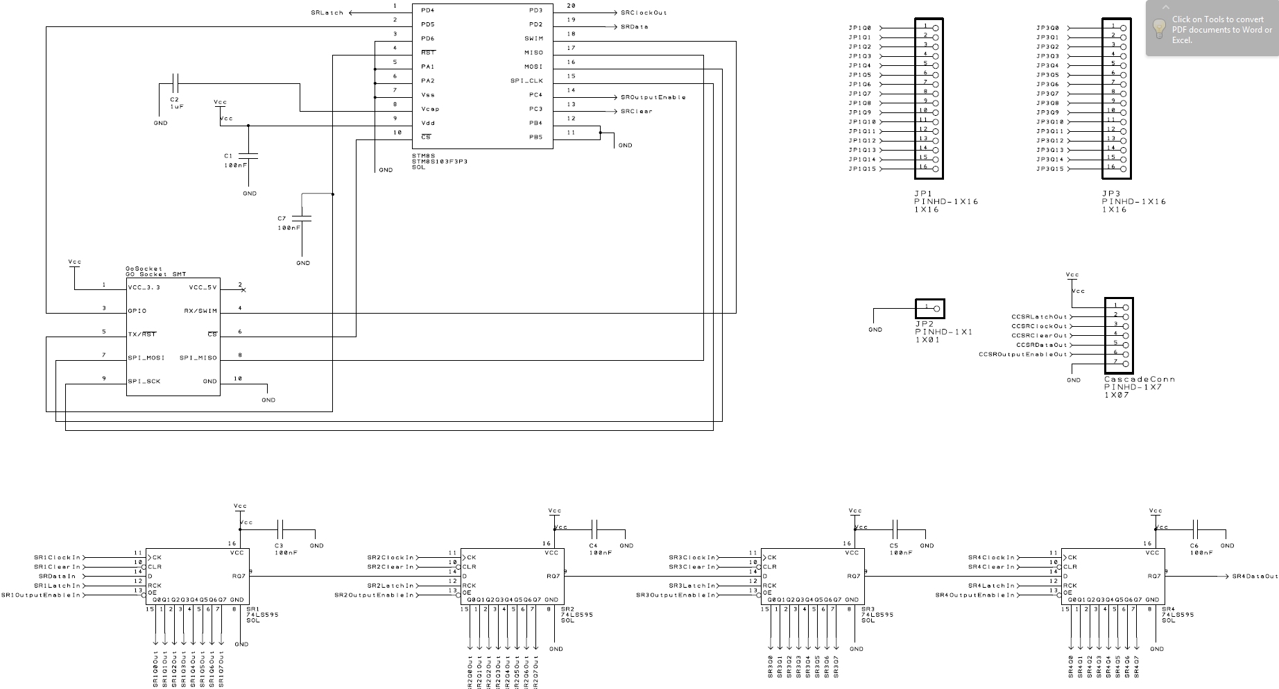
Schematic
PCB Layout
The PCB layout process converts the schematic into a representation of the board which can be edited using the PCB layout tools. The layout can appear confusing as it is a layered version of the final board. Different colours map to the layers / artefacts on the board. It is this layering which can appear confusing at first.
The layout process requires the following tasks to be completed:
- Conversion of the schematic into the ratsnest
- Reorganising the components in the ratsnest to their “final” position on the board
- Routing the tracks between the components
- Addition of additional artefacts such as text
- Design Rule Checks (DRC) and verification of the layout
- Production of the manufacturing files
It is suggested that the above process is completed in order as each step adds new artefacts to the board.
As noted earlier, the schematic and related files are being created using DesignSpark PCB. The processes being discussed are relevant to PCB manufacture in general.
Making the Ratsnest
The first step in the process is to convert the schematic into a PCB layout. Often this process creates a ratsnest of components and connections with no real layout:
The ratsnest in DesignSpark’s PCB editor shows each component in the footprint it will occupy on the final board. The logical connections between the components are also shown as simple lines between the pads which will be used to mount the components. The lack of structure of the output gives the representation it’s name as it looks like a disorganised rats nest.
Placing the Components
The next step is to lay out the components out on the board. DesignSpark PCB converts the Schematic into a disorganised layout. The Output Expander board is a simple board and reorganising the layout should be simple. The layout can be broken down into the following functional units as follows:
- Connectors
- Shift registers
- Microcontroller
The connectors should near to the edge of the board to allow the board to be connected to the Netduino GO! and external circuitry with ease.
The shift registers and microcontroller can be placed anywhere on the board as we are looking at a low speed, simple board. Placement is more critical for more complex boards. For this board it is logical to place the shift registers near the output from the board as they will used to provide the 32 outputs for the board. It is also logical to place the microcontroller near the Netduino GO! connector as it is receiving instructions from the Netduino GO!.
There are also a number of passive components on the board. These provide some signal filtering and power stabilisation. These components should be place as close to the chip they are supporting. For instance, each of the shift registers has a 100nf capacitor between power and ground. This capacitor provides a buffer for power spikes and it should be placed a close to the chip as possible. There are similar capacitors near the STM8S microcontroller.
So the first step is to take the components and break them down into the logical groups. You can then deal with each group in turn.
The following shows the start of the component placement:
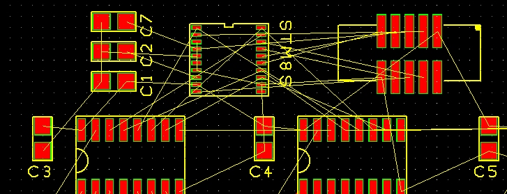
Components on PCB
The major components are shown along with the connections between the components. This appears a little disorganised at the start as the yellow lines showing the connections between the components run in a straight line taking the most direct route.
Routing the Tracks
Routing is the process of placing copper connections between the components. So at this point you should have the components in their final resting place. If you have to move them later then you will disturb the routing. It is not too big a problem as you can always break the connection and then re-establish it with a new copper track.
The next thing to consider is that for this simple board there are two types of tracks, power and signal. In DesignSpark PCB these are also broken down into two subcategories, nominal and minimum. Where possible I have always selected the nominal connection for both power and signal. You should also remember that it is possible it define your own track type.
When connecting components DesignSpark PCB is reasonably intelligent and will take the connection type from the schematic and apply this to the PCB layout. By default this will be the nominal connection for either power or signal.
Like many PCB layout packages, DesignSpark PCB provides an auto-router. In my experience these take a long time to run and does not always provide a complete board (i.e. they fail to completely route the board) and they also need a reasonable amount of computing power to complete. For a small and simple board like this one I have always found that manually routing the board is the preferred option.
Routing also requires a change in the way of thinking about the board. PCB manufacture is a multi-layer process. The simplest for home manufacture is a single layer. This board can use two layers as this is relatively standard for low cost. Two and four layers are becoming common in the low cost prototype market. Larger numbers of layers are also possible but are currently too expensive and complex for the hobbyist. The simplicity of this board only merits a two layer board which also helps to keep the production cost lower.
Time to start routing…
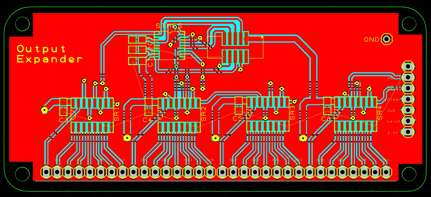
After a while the board started to come together:

Partially Routed
The above image shows the partially routed board with some additional artefacts to give an indication how the final board will look. Some important points to note:
- Red traces are tracks which will appear on the top layer of the board.
- Cyan traces are tracks which are on the lower layer of the board.
- Thick tracks are used to carry the ground and power signals.
- Thin tracks carry signals between components.
- Small yellow circles in the tracks are vias (interconnections between the top and bottom layer of the board).
- Component outlines are shown in yellow. These represent the physical size of the component when it is mounted on the board. This will also appear on the top layer silkscreen.
- The green parts are represent the board outline and the mounting holes for the board.
- All of the changes in direction of a track are mitred rather than simple right angles.
You can see that the board still contains some very thin yellow lines from the original ratsnest. These lines represent the connections which have not been routed yet. A quick check of the connections shows that all of these pads are connected to ground. These pads will become connected when the ground plane is added to the board.
The final routing task is to add a ground plane to the top and bottom of the board.
Top Layer With Ground PlaneTopLayerWithGroundPlane
Adding Additional Artefacts
Now the routing is complete we can return to the additional artefacts on the board. The first and possibly the most important is the board outline. The original outline in the image above was used to give an indication of the maximum ideal board size (10cm x 5cm). Most of the Netduino GO! modules released so far have had rounded corners. So the board outline was replaced by a board with rounded corners.
The next check was to look at the silkscreen layers. These already contain the component outlines along with some names. Some useful additional information includes pin names for the connectors along with some information about the board – a name perhaps.
A final note about the mounting holes. These should be placed on a 5mm x 5mm grid in order to achieve GO! certification. The holes should also be 3.1mm – 3.3mm in diameter.
One limitation I found with DesignSpark PCB is the fact that you cannot place a logo/image in the silkscreen layer (or any other layer for that matter). This is a major limitation of the package. It appears that the solution is to create a font containing the image and then add text to the silkscreen using the font which has been created. For a package which is currently at version 5 seems to be a major omission.
DRC and Verification
The final step in the design process before going to manufacture is to verify the board and determine if the board can be manufactured successfully.
Firstly, print out the board. Now double check the connections making sure that all of the pads are connected correctly. A print out is more useful to me as I can take it away from the screen and start to tick off the pads I believe to be connected correctly.
Now for the DRC check. By default DesignSpark PCB has a set of design rules built in. These rules represent manufacturing parameters such as:
- Track thickness
- Minimum spacing between tracks
- Minimum distance of a component from the board edge
The list is much larger but you get the idea.
I found that the values used for some rules was too cautious and would not let me route some tracks correctly. I had to change the default rules using values from the manufacturer I had decided to use. Rerunning the check with the new minimum values for track spacing allowed the board to pass DRC.
Generate Manufacturing Files
PCB manufacturers use Gerber files. The exact specification of the files used is determined by the chosen manufacturer. For this board we will need to generate a Gerber file in RS-274x format for the following layers:
- Top layer: pcbname.gtl
- Bottom layer: pcbname.gbl
- Solder Stop Mask top: pcbname.gts
- Solder Stop Mask Bottom pcbname.gbs
- Silk Top: pcbname.gto
- Silk Bottom: pcbname.gbo
- NC Drill: pcbname.txt
One thing to note is that there is nothing to represent the board outline. This has been added to the top silkscreen layer as requested by the manufacturer I have chosen.
The Gerber files are simple text files which contain instructions for the CNC machines used in the manufacturing process.
Now we have the Gerber files it is useful to check that they look right. Luckily there is an on-line Gerber viewer. Uploading your files will allow you to check that the image generated matches the design and layout.
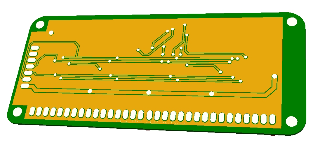
3D View
A neat little feature of DesignSpark PCB is the ability to generate a 3D view of the board being made and to rotate the view. A quick check gives the following images for the final board:
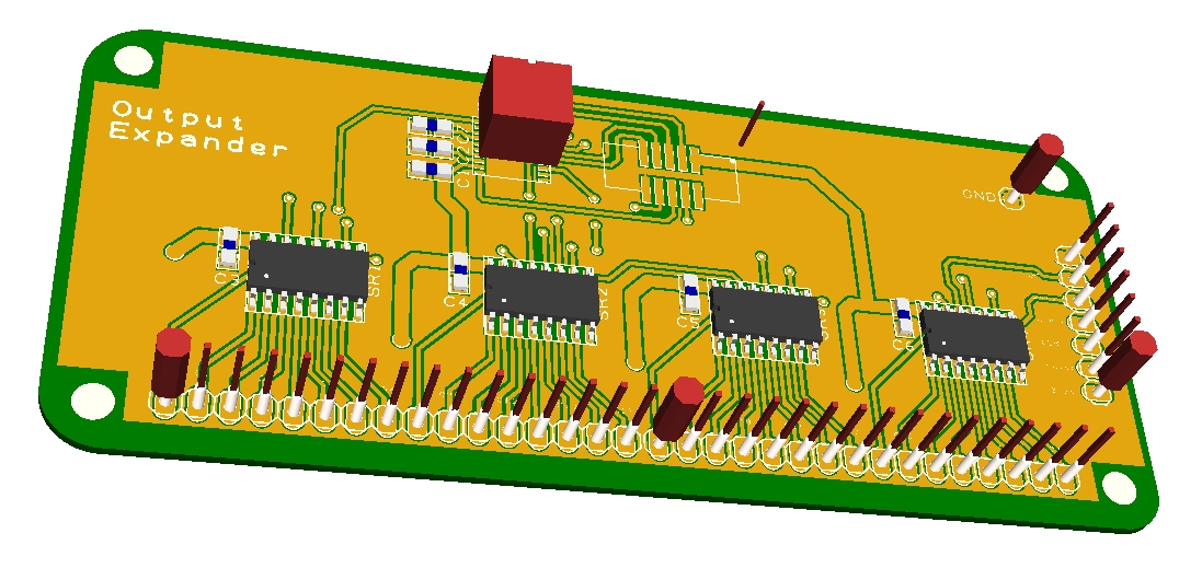
Top of Board in 3D
Note that the GND pin to the top right of the board has four tabs connecting it to the ground plane.
The cube hovering above the board is the 3D model for the STM8S. A better model could be created, more along the lines of the 75HC595 shift registers. A task for another day…
And rotating the board to view the underside we see the following:
Bottom of Board in 3D
PCB Prototype Manufacturer
The past 12 months have seen a number of PCB companies offer a low cost prototype PCB service. These services allow the production of a number of board (typically 10) starting as low as $10 for 10 5cm x 5cm boards. Some services even give you extra boards if you open source the hardware and hence allow them to add the board to their online shop.
Companies offering this type of service include:
The number of PCB options may be limited (i.e. silkscreen colour etc.) but this certainly makes the cost of production viable. For instance, a 5cm x 10 cm board costs less than $30 including shipping to the UK for 10 boards. Our module has been designed to just fit within the 5cm x 10 cm footprint.
Another service for the hobbyist or prototype developer is that offered by Batch PCB. This company collects the production files from customers and creates a single panelised board containing one or more customer designs. This board is manufactured, the individual boards cut and extracted for shipping to the customer. By doing this the company can offer a low cost production service ($2.50 per square inch at the time of writing) for larger boards.
There are a number of other companies offering low cost services for small runs. The companies quoted are ones I have noted over the past few months when I have been looking for low cost alternatives.
Conclusion
There will now follow a slight pause in the development of the hardware while the boards are produced somewhere in China. According to colleagues it typically takes about one week for manufacture and two weeks for shipping.
This does not mean that development needs to stop. On the assumption that the prototype will work correctly we still have the following tasks which can be completed:
- Order the components for mounting on the board
- Develop the drivers
In the next post we will look at developing the drivers for the board using the breadboard prototype as our test environment.